GE-International Journal of Engineering Research
Vol. 4, Issue 7, July 2016 IF- 4.721 ISSN: (2321-1717)
© Associated Asia Research Foundation (AARF) Publication
Website: www.aarf.asiaEmail : [email protected] , [email protected]
LOW POWER VLSI IMPLEMENTATION OF PSEUDO RANDOM
SEQUENCE GENERATOR
Mrs. Jyoti M Roogi ECE Department CMR Instititute of Technology, Bangalore
Mr. Chetan H. ECE Dapartment CMR Istitute of Technology,
Bangalore
Mrs. Bhumika Narang TCE Department CMR Istitute of Technology,
Bangalore
ABSTRACT
A mixed signal technique for designing self-testable VLSl circuits, characterized by low power consumption and Maximum testing speed, is proposed. An original feature of this PN sequence generator technique is the procedure used for Synthesis of test pattern generation. Its objective is to design Mixed-mode generator of minimal complexity that maximize the fault sensitizing ability of test sequences produced within the allowable test running time.
Keywords—Linear Feedback Shift
Registe(LFSR),Phase Lock Loop( PLL), Circuit under Test,
I. INTRODUCTION
As the density of VLSI products increases, their testing A becomes more difficult and costly. Generating test patterns has shifted from a deterministic approach, in which a testing pattern is generated automatically based on a fault model and an algorithm, to a random selection of test signals. No matter whether deterministic or random generation of testing patterns is used, the testing pattern applied to the VLSI chips can no longer cover all possible defects. Therefore, the question of sufficient testing needs to be explored in detail. Consider the manufacturing processes for VLSI chips: two kinds of cost can incur with the test process, the cost of testing and the cost of accepting an imperfect chip. The first cost is a function of the time spent on testing or, equivalently, the number of test patterns applied to the chip. The cost will add to the cost of the chips themselves.
The second cost represents the fact that, when a defective chip has been passed as good, its failure may become very costly after being embedded in its application. An optimal testing strategy should trade off both costs and determine an adequate test length (in terms of testing period or number of test patterns).
testing easier (e.g., making it possible to conduct test generation and test application in practical time) and/or more efficient (e.g., making it possible to reduce test data and/or test time).
Recently, power dissipation during testing, i.e., test power, has emerged as a new threat to the quality and costs of VLSI testing, especially for low-power circuits. The reason is that test power can be much higher than functional power. Excessive test power may cause heat damage and circuit malfunction. If left uncontained, test power may lower test quality due to over-test; if inefficiently managed, test costs often increase. Therefore, low-power testing is indispensable to modern low-power VLSI circuits. In order words, no matter how attractive a low-power circuit design is, it cannot be realized without low-power testing. In the rest of this paper, basic concepts used in test generation and design for testability will be reviewed. Based on that, the impact of test power is described. The purpose is to highlight the need for low-power VLSI testing.
II. BASICS OF TEST GENERATION AND
RANDOM TESTING
Test generation is the process of creating test patterns for a circuit-under-test or CUT. The ultimate goal is to determine whether the CUT is free of any manufacturing defects by applying test patterns and comparing measured test responses with expected test. Applying individual patterns to individual circuit is quite a complex task for a chip with billions of components on it. For this context Random Testing is quite a feasible solution provided for Testing.
Random testing (RT) is a fundamental testing method which simply selects test cases in a random manner from the whole input domain. Random Testing has been popularly applied to assess hardware and software reliability. However, its effectiveness at detecting failures is debatable.
Random testing is a basic testing technique, motivated by the observation that neighboring inputs normally exhibit similar failure behavior. The approach of Adaptive Random Testing has recently been proposed to enhance the fault detection capability of random testing. The intuition of adaptive random testing is to evenly spread the randomly generated test cases. Experimental results have shown that adaptive random testing can use as fewer as 50% of test cases required by random testing with replacement to detect the first failure. These results have very significant impact in hardware
testing, because random testing is a basic and popular technique in hardware testing.
III. PATTERN GENERATOR USING LFSR AND
PLL
A novel pattern generator has been implemented by using LFSR (Linear Feedback Shift Register) and PLL (Phase Locked Loop). Block Diagram of PLL is shown in Fig. 1. Here, different signals with known frequencies are generated from PLL, which is driven by LFSR for Pseudo Random sequence generation through Decoder. LFSR is designed with D flip flops and XOR gate. The pseudo random signal is generated with particular primitive polynomial. The randomness of sequence depends on polynomial selected. Then the optimized PLL is selected for generation of signal with known frequencies that is triggered by decoder.
This PLL is can be further used to test different devices for testing and triggering of any external devices.
Use of Linear Feedback Shift Register is being the key component of built in self test environments. LSFR’s error detection and error correction properties make them a prime constraint of design for testability. Basically LSFRs are capable of generating exhaustive and/or random vectors through different environments.
Fig. 1 Linear Feedback Shift Registers (LFSR)
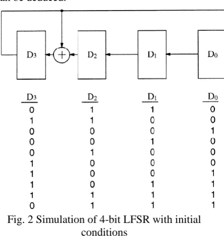
[image:3.595.310.557.90.168.2]Here equivalence exits between the two structures in the sense that knowing the properties of the first structure, second structure can be deduced.
Fig. 2 Simulation of 4-bit LFSR with initial conditions
Simulation of 8 – Bit LFSR is shown in fig. 3. If we initialize the shift register to a nonzero state i.e. 0110, and shift register a number of times, the LFSR goes through a number of states and a sequence of binary vector can be generated through it. For certain configuration of LFSR, these sequences can be pseudo random. Fig. 4 is showing the example of adding input to an LFSR and shift in a serial stream of input. This can compress the stream of inputs to the length of LFSR. These contents of LFSR can be formed the signature of the serial input stream which is known as data compression capability which can be used in Fault Signature Analysis. LFSR can also be configured to multiply and divide
[image:3.595.77.299.311.545.2]polynomials of binary vectors with binary coefficient. This ability can be used to encode and decode error correcting and detecting codes for ex. cyclic redundancy check codes (CRC).
Fig. 3 LFSR with specified input
A Decoder can be employed with LFSR with primitive polynomial to trigger PLL to generate different signals with desired frequency. A novel approach has been implemented to design pesudo random sequence generator based on the criteria disscussed above.
Phase Lock Loop (PLL) is proposed for generation of multiple clock signals in system on chip design shown in fig. 5. When a device reads a digital data stream, it needs an input clock to know where to read each bit from the stream. This is easy enough if there are two separate data lines--one for the actual data, one for the clock to time that data--but there are several types of data stream which are sent with no clock information, including many types of telecommunications transmissions, as well as the data that comes from a disk drive's read head. When user has a signal like this, it must synthesize or "recover" the clock for that signal. This can be a bit complex, because its shows how fast the clock is and where its transitions are. Many clock recovery circuits simply use a PLL for clock recovery, configuring the center frequency of the PLL's VCO to the actual frequency of the data stream, and then using the data stream as the external input to the phase detector.
Fig. 4 Phase Lock Loop (PLL)
[image:3.595.312.522.568.648.2]process, a bit-encoding standard is usually used that minimizes gaps in which the data stream fails to transition.
IV. SIMULATION RESULTS
A. Simulation Environment
All the circuits have been simulated on 90nm technology on cadence tool. To establish an impartial testing environment each circuit have been tested on the same input patterns.
B. Simulation Results
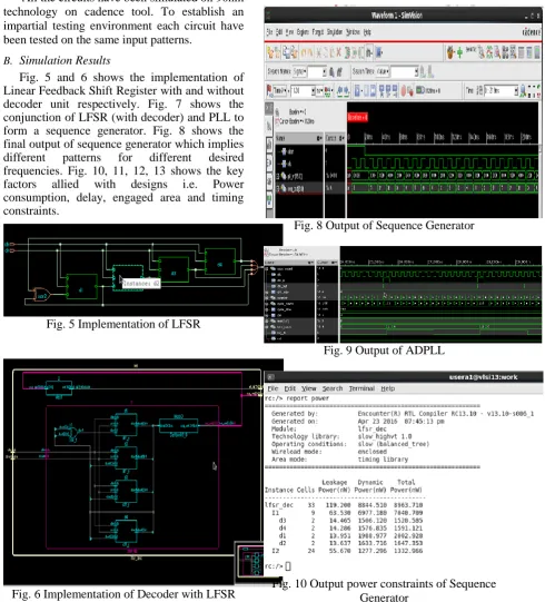
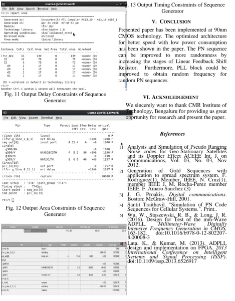
Fig. 5 and 6 shows the implementation of Linear Feedback Shift Register with and without decoder unit respectively. Fig. 7 shows the conjunction of LFSR (with decoder) and PLL to form a sequence generator. Fig. 8 shows the final output of sequence generator which implies different patterns for different desired frequencies. Fig. 10, 11, 12, 13 shows the key factors allied with designs i.e. Power consumption, delay, engaged area and timing constraints.
[image:4.595.307.561.40.100.2]Fig. 5 Implementation of LFSR
Fig. 6 Implementation of Decoder with LFSR
Fig. 7 Implementation of Sequence Generator
Fig. 8 Output of Sequence Generator
Fig. 9 Output of ADPLL
[image:4.595.69.560.134.676.2]Fig. 11 Output Delay Constraints of Sequence Generator
[image:5.595.70.540.33.635.2]Fig. 12 Output Area Constraints of Sequence Generator
Fig. 13 Output Timing Constraints of Sequence Generator
V. CONCLUSION
Presented paper has been implemented at 90nm CMOS technology. The optimized architecture for better speed with low power consumption has been shown in the paper. The PN sequence can be improved to more randomness by increasing the stages of Linear Feedback Shift Resistor. Furthermore, PLL block could be improved to obtain random frequency for random PN sequences.
VI. ACKNOLEDGEMENT
We sincerely want to thank CMR Institute of Technology, Bengaluru for providing us great opprtunity for research and present the paper.
References
[1] Analysis and Simulation of Pseudo Ranging
Noise codes for Geo-Stationary Satellites and its Doppler Effect ACEEE Int. J. on Communications, Vol. 03, No. 03, Nov 2012.
[2] Generation of Gold Sequences with
application to spread spectrum system. F. Rodriguez(1), Member, IEEE, N. Cruz(1), member IEEE J. M. Rocha-Perez member IEEE. F. Amaro Sanchez (3)
[3] J. G. Proakis, Digital communications.
Boston: McGraw-Hill, 2001.
[4] Santit Traithavil. "Simulation of PN Code
Sequences for Cellular Systems.". Print..
[5] Wu, W., Staszewski, R. B., & Long, J. R.
(2016). Design for Test of the mm-Wave ADPLL. Millimeter-Wave Digitally Intensive Frequency Generation in CMOS, 163-182. doi:10.1016/b978-0-12-802207-8.00008-3
[6] Lata, K., & Kumar, M. (2013). ADPLL