Pausible Clocking Based Heterogeneous Systems
Kenneth Y. Yun, Member, IEEE
Ayoob E. Dooply, Student Member, IEEE
Abstract—
This paper describes a novel communication scheme, which is guaran-teed to be free of synchronization failures, amongst multiple synchronous and asynchronous modules operating independently. In this scheme, com-munication between every pair of modules is done through an asynchronous FIFO channel; communication between a module and the FIFO is done using a request/acknowledge handshaking. Synchronization of handshake signals to the local module clock is done in an unconventional way [1], [2], [3], [4] — the local clock built out of a ring oscillator is paused or stretched, if necessary, to ensure that the handshake signal satisfies setup and hold time constraints with respect to the local clock. In order to validate this scheme, we implemented a test chip in0.5µmCMOS. This chip is designed as a ring, composed of two synchronous modules, an asynchronous module, and two asynchronous FIFO’s. Each module functions as a receiver to one module and a sender to another module. Test results show that the chip functions reliably up to 456MHz.
Keywords— Globally asynchronous locally synchronous, Stretchable
clock, Synchronization, Heterogeneous systems
I. INTRODUCTION
The next generation digital VLSI systems will necessarily be based on system-on-a-chip concepts, in order to satisfy unre-lenting demands for higher performance and also to accommo-date smaller packaging and low power requirements. These on-chip systems will consist of multiple independently syn-chronized modules: some may be clocked modules, such as synchronous processor cores, while others may be clockless (asynchronous) modules, such as peripheral controllers. These chip designs will resemble today’s complex board-level designs. On-chip modules will be held together by interface glue logic which must facilitate high speed communication between syn-chronous modules operating at different clock frequencies, be-tween synchronous and asynchronous modules, and bebe-tween asynchronous modules. The key difference between today’s board-level designs and the future system-on-a-chip designs, however, is the speed at which communications take place.
A first step toward such heterogeneous system design on a chip is a reliable high-speed communication scheme among multiple synchronous modules operating independently. We ex-amined a variety of communication schemes that attempt to mit-igate synchronization failure without sacrificing communication throughput. They generally fall into one of two categories: (1) brute-force synchronization of communication signals to each module’s free-running clock with an acceptable level of syn-chronization failure; (2) adjustment of individual synchronous module’s local clock, when necessary, to avoid synchronization failure.
The first category includes methods such as the well-known latching scheme and a natural extension of the double-latching scheme called pipeline synchronization [5]. These methods reduce the probability of synchronization failure to
This work was supported in part by a gift from Intel Corporation and by a National Science Foundation CAREER Award MIP-9625034.
The authors are with ECE Dept., University of California, San Diego, 9500 Gilman Drive, La Jolla, CA 92093-0407; email:{kyy,adooply}@ucsd.edu.
an acceptable level by resynchronizing communication signals with back-to-back latches. These methods are simple and inex-pensive to implement, but a major drawback is the latency of communication.
The methods in the second category [1], [2], [3], [4] generally rely on stopping or stretching each synchronous module’s lo-cal clock to guarantee that communication signals never violate setup and hold time constraints with respect to the local clock. Although these methods are robust and do not incur long com-munication latency, they involve designing a special clocking circuit, unfamiliar to most designers. The simplest example us-ing this scheme one can conceive is a synchronous module com-municating with an asynchronous peripheral. In this system, the synchronous module latches the handshake signals from the asynchronous module by stopping or stretching its own clock, when necessary.
Both categories described above require some form of arbitra-tion. However, if the phase relation between two synchronous modules can be predicted deterministically as in [6], then we can avoid synchronization failure, without arbitration, by timing communications when safe.
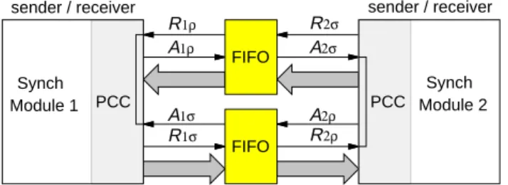
In this paper, we describe a general method of communi-cation amongst multiple synchronous and asynchronous mod-ules operating independently, i.e., at different clock frequencies or phases, based on the pausible clocking scheme as shown in Fig. 1. Synchronous modules communicate with one another via asynchronous FIFO’s1 used as communication channels. The interfaces between the synchronous modules and the FIFO are pausible clocking control (PCC) circuits.
In order to validate this scheme, we implemented a test chip in0.5µm CMOS through MOSIS. This chip is designed as a ring, composed of two synchronous modules, an asynchronous module, and two asynchronous FIFO’s. Each module functions as a receiver to one module and a sender to another module. Each synchronous module has a frequency control with four settings, which is independently programmable externally. The chip functions reliably for all the settings, albeit substantially faster than expected by simulation.
II. DESIGN OFPAUSIBLECLOCKINGCONTROL
The pausible clocking control is a scheme to avoid synchro-nization failure by adjusting the local clock. A synchrosynchro-nization failure at the module interface occurs when the arrival times of an external signal transition and a sampling edge of the clock are indistinguishable by the sampling latch at the module boundary. In our scheme, the synchronization failure is circumvented by pausing or stretching the local module clock when necessary.
1Self-timed FIFO’s have been used to facilitate robust communication be-tween synchronous modules operating at the same frequency elsewhere [7]. However, they have not been utilized in communication between synchronous modules operating independently at different clock frequencies.
sender / receiver sender / receiver R1ρ A1ρ A1σ R1σ R2σ A2ρ R2ρ A2σ FIFO FIFO Synch Module 2 PCC Synch Module 1 PCC
Fig. 1. Two synchronous modules communicating via asynchronous FIFO channels. sysclk Ring Oscillator Rρ Aρ Rσ Aσ ME rclk AFSM AFSM Arbiter FSM sysclk R1 G1 R2 G2 R G ρ SR FSM SAσ Fig. 2. PCC. A. Synchronization Strategy
A block diagram of the PCC is shown in Fig. 2. This scheme uses a mutual exclusion element (ME) to force the temporal sep-aration of the sampling edges of the clock and external signal transitions. A mutual exclusion element [2], [8] is a circuit that allows one request to pass through at a time on a first come first serve basis. When two inputs arrive simultaneously, it selects one to pass through arbitrarily. Because MEs require that re-questers competing for shared resources must be persistent, the clock input to the ME must be “stretched” when it loses an ar-bitration. A ring oscillator is used instead of a crystal oscillator in order to be able to adjust the duration of off-phases of the clock. The local module clock, sysclk, is a buffered version of one of the outputs of the ME. It normally has a 50% duty cycle, except when the clock input loses an arbitration, in which case an off-phase of the clock is stretched.
Consider a scenario in which a synchronous module equipped with the PCC is receiving inputs from the FIFO. The PCC needs
Rρ R1 R G1 SRρ Aρ rclk sysclk Aσ R2 G setup sysclk paused
Fig. 3. PCC timing (bidirectional communication).
an arbiter, as depicted in Fig. 2, to decide which of the two inde-pendent inputs (the request from the sending FIFO [Rρ] and the acknowledgment from the receiving FIFO [Aσ]) to be presented to the ME. For this scenario, we assume thatRρ has won the arbitration. Thus, in this case, the arbiter simply forwardsR1 to the ME andGfrom the ME. As shown in the shaded area of Fig. 3,Rρ is forwarded to the ME via the asynchronous finite state machine (AFSM) and the arbiter.
If rclk is low whenRrises, then the ME immediately raises
G, which prompts the AFSM to generate an event onSRρ. This event is effectively synchronized to sysclk, i.e., guaranteed not to induce a synchronization failure when sampled by the FSM, under a reasonable timing assumption as described below. Note that rclk may rise before the ME lowersG, but the ME will not allow sysclk to rise untilGbecomes low.
On the other hand, if rclk is already high whenR rises, the assertion ofGis stalled until rclk is lowered. As soon as rclk falls, the ME raisesGand the AFSM generates an event onSRρ. Rclk may actually rise at about the same time R rises. In such situations — the situations in which temporal separation ofR+andrclk+becomes blurred — the ME simply “tosses a coin” to determine which signal to service first. Ifrclk+wins the “coin toss”, then sysclk rises first andGremains low until sysclk falls (which happens shortly after rclk falls). On the other hand, ifR+wins, then the ME raisesGfirst and blocks sysclk from rising. In order to prevent sysclk from stalling indefinitely (until the next toggling of the request,Rρ), the AFSM lowers
R1 immediately afterG1 rises, which in turn causesGto fall allowing sysclk to rise.
The PCC does not differentiate rising edges of Rρ from falling edges — both edges enableR1to be asserted andG1to be asserted as a result. In fact, the AFSM effectively performs a two-phase to four-phase conversion fromRρtoR1and a four to two-phase conversion fromG1toSRρ. This conversion is in-dependent of whether a two-phase or four-phase communication protocol is used between the FIFO and the synchronous module. It is merely done so that both edges ofSRρare synchronized to sysclk.
In order for the synchronous FSM that generatesAρ to rec-ognize the change inSRρ, we need to ensure thatSRρsatisfies setup and hold time constraints with respect to sysclk. In or-der to recognizeSRρ+(SRρ−)2 reliably, the path fromG
1+ toSRρ+(SRρ−) must be shorter than the path fromG1+to
sysclk+viaR−andG−by at least the data setup time for the FSM latches. This is easily satisfied in practice becauseG1+ toSRρ+(SRρ−) delay is a complex gate delay (transitions on
SRρare directly triggered byG1+), which is much less than the delay fromG1+toR−toG−tosysclk+.
The asynchronous finite state machine (see Fig. 4) is speci-fied in burst-mode [9] and synthesized using the 3D-gC synthe-sis tool [10]. This burst-mode state machine has two inputs (Rρ,
G1) and two outputs (R1,SRρ). In state 0, whenRρrises, the
machine raisesR1and goes to state 1. In state 1, the machines waits forG1to rise; when it does, the machine lowersR1 and raisesSRρconcurrently and goes to state 2. WhenG1 falls in state 2, the machine transitions to state 3. The machine
0 1 2 3 / 1 G− /R1+ + Rρ / 1 G− /R1+ Rρ− 4 5 / + 1 G R1− / + 1 G R1− + ρ SR − ρ SR R1 1 G reset 1 G 1 G Rρ weak ρ SR ρ SR SRρ weak
Fig. 4. PCC asynchronous finite state machine specification and implementa-tion.
tions through states 4 and 5 and back to 0, asRρ−triggers a sequence of signal transitions ending withG1−.
B. Arbitration
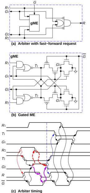
In order to simplify the interface to the ME, our design uses an arbiter to select just one external signal to pass through at a time. An arbiter [8], [11], [12] is a circuit that propagates one request at a time (as does the ME) but also acknowledges the requesters with grant signals as well.
The arbiter used in our design [13] shown in Fig. 5 is different from conventional ones. WhenR1orR2 arrives at the arbiter, the arbiter forwards a request to the ME, without determining which one has arrived first. As shown in Fig. 3, R1 and R2 (enabled by Rρ and Aσ respectively) may arrive at the same time, causing gME(gated ME inside the arbiter) to go into a metastable state. WhenR+arrives at the ME,rclk+may also arrive at about the same time as well. If the ME determines that
R+has arrived first (after resolving its internal metastability), it raisesGand blocks sysclk from rising (thus stretching it) untilR falls. Note that the metastability resolution in thegMEwould be well underway, if not already finished, by the timeGis asserted. Thus the metastability resolution in thegME and the ME are done concurrently. WhenGis asserted,G1rises, which in turn resetsRandR1.R−enablesG−, which in turn enables sysclk to rise. The pending requestR2enablesRto be asserted again afterG1resets. However, it is blocked until rclk falls.
Note that our arbiter design is not speed-independent, i.e., it requires a timing constraint on its environment for correct func-tionality. Consider an example depicted in Fig. 5(c), in which
R2+starts a chain of events, starting withR+. AfterGis as-serted,G2is raised. This event enables bothR−andR2−. IfR2 side is slow to respond, i.e.,R2does not fall tillGis negated, then this residual R2 may be viewed as a new request to the gME. In our design, the ASFM (see Fig. 4) lowersR2 imme-diately, onceG2rises, in order to prevent this problem. More precisely, the following timing constraint is always satisfied for bothi= 1and2:
tG+
i→R−+tR−→G++tG+→G−i > tG+i→R−i . (1)
(a) Arbiter with fast−forward request
(b) Gated ME R1 G2 R2 G 1 G 1 G 1 T T2 G2 gME (c) Arbiter timing R G R1 1 G 1 T R2 T2 G2 R1 1 G G2 R2 R G gME
Fig. 5. (a) Fast-forward arbiter; (b) Gated ME (ME with enabled outputs); (c) Fast-forward arbiter timing.
III. SYSTEMCONFIGURATIONS ANDLIMITATIONS
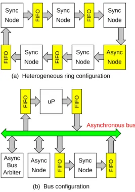
Using the pausible clocking scheme, it is conceivable that one can construct a heterogeneous multi-processor system with point-to-point links between every pair of nodes. Each link is a bidirectional FIFO as shown in Fig. 1. However, as fanouts from and fanins to each node increase, the arbiter block becomes larger making the system design impractical.
However, we assert that it is possible to construct a ring con-figuration as shown in Fig. 6(a) similar to the systems proposed in Scalable Coherent Interface (SCI) specification [14]. In this structure, messages are always transmitted to one side and re-ceived from the other side, so that only one level of arbitration is required in the PCC. A major advantage of our ring configu-ration over other proposed systems, such as SCI system, is that it is a truly heterogeneous system with each node operating at its own speed.
Another possible system configuration would be a conven-tional bus based architecture depicted in Fig. 6(b). In this
config-uP Async Node FIFO FIFO FIFO Node Sync FIFO (b) Bus configuration FIFO FIFO FIFO Node Sync FIFO Node Sync Node Sync Async Node Node Sync Node Sync
(a) Heterogeneous ring configuration
Async Bus Arbiter
Asynchronous bus
Fig. 6. (a) A heterogeneous message-passing multiprocessor using PCC’s; (b) A conventional bus based system.
uration, synchronous modules are connected to an asynchronous bus, e.g., Futurebus+, via FIFO’s and asynchronous modules are connected directly to the bus. Since the synchronous modules in this configuration interface to the bus only via two FIFO’s, the PCC’s in the synchronous modules require just one level of ar-bitration.
Systems-on-a-chip should be designed with as many reusable components as possible. Standard modules, such as CPU cores, should be reused with little or no modification, because these modules are highly optimized for performance and sensitive to timing variation. For the systems proposed in this paper, ide-ally, the pausible clocking control circuit should simply replace a portion of the system clock generation unit. However, for state-of-the-art microprocessors, the system clock is produced by a phase locked loop (PLL). We cannot adjust the phase of the output of a PLL instantaneously in an analog fashion, as re-quired in our pausible clocking control. Thus a ring oscillator should be used in place of a PLL. We then lose control of the nominal frequency. Tuning the ring oscillator frequency would require more control pins and hence is more expensive. Further-more, the ring oscillator based clocks may be more susceptible to jitter problems. However, the ring oscillator does have an ad-vantage that its frequency drift closely tracks logic components on the chip, e.g., if logic components slow down due to an in-crease in operating temperature, then so does the ring oscillator.
IV. PERFORMANCECONSIDERATIONS
In this section, we examine performance limitations of our PCC scheme. The maximum clock frequency of the PCC is constrained by the FSM input setup and hold time require-ments as follows (see Fig. 7). Assume thatRis high (enabled by Rρ) whenrclk falls. This activates G+and G1+in se-quence, which in turn enablesSRρ to toggle. We need to
in-sysclk Ring Oscillator Rρ Aρ Rσ Aσ ME rclk AFSM AFSM Arbiter FSM sysclk R1 G1 R2 G2 R ρ SR FSM SAσ G G (1) (2) (3)
Fig. 7. Performance constraints.
sure thatSRρ satisfies setup and hold time requirements with respect to sysclk+. Assuming that the delays through paths (1) and (2) aret1 = trclk−→G++tG+→G+
1 +tG+1→SR+ρ and t2 =trclk+→sysclk+ respectively, the following inequality must
hold true:
−T2 +th< t1−t2< T2 −tsu (2) wheretsu andthare the required setup and hold times ofSRρ with respect tosysclk+andT is the nominal period of the ring oscillator clock with a 50% duty cycle. Therefore, the minimum clock period achievable is:
Tmin= 2 max(t1−t2+tsu, t2−t1+th). (3) In general,t2>> t1for a large clock tree; henceTmin= 2(t2−
t1 +th). In other words, the minimum clock period is about twice the clock tree delay.
Assuming that∆s+ ∆hrepresents the metastability window of the ME (analogous to the setup and hold time window of a flip-flop) and∆represents the delay from the timeRis granted an access to the ME to the time it relinquishes it, we can de-fine “window of vulnerability” to be∆ + ∆h (if∆ >∆s). In other words, sysclk may pause (due toA+σ enabled byRσ+) if the following condition is true:
nT−∆ < tsysclk+→R+ σ +tR+σ→A+σ +tA+σ→R+2 +tR+2→R+ +trclk+→sysclk+ < nT+ ∆h forn≥1, (4) where∆ =tR+→G++tG+→G+ 1 +tG+1→R−. A similar
inequal-ity exists forRρ(the same as Eq. 4, but withRσreplaced byAρ,
AσbyRρ, andR2byR1).
Clearly, the frequency and duration of clock stretching de-pends on the size of this window (∆ + ∆h) — the smaller this window, the higher the performance of the system.
V. EXPERIMENTALRESULTS
We constructed a heterogeneous ring on a chip as depicted in Fig. 8. The chip consists of two synchronous modules nicknamed “CPU” (CPU) and “Co-processor” (Coproc), an asynchronous module (Async), and two asynchronous FIFO’s (FIFO1andFIFO2).3 Every module has two neighbors. Mes-sages are always transmitted to one side and received from the
Async CPU FIFO1 FIFO2 R A R A A R A R A R Coproc 0 0 1 1 2 2 3 3 4 4 4 4 2 2 4
Fig. 8. Test chip configuration.
R2A1 =00 R2A1 =11 R2A1 =01 R2A1 =01 R1A2=01 R1A2=10 R1A2=11 R1A2=11 R1=0 A2=0 R1=1 A2=1 R1=0 A2=0 PCC Coproc FSM FF Rρ Aσ SRρ SAσ R1 R2 A1 A2 sysclk Rin Aout Rout Ain Din Dout (a) (b)
Fig. 9. (a) Co-processor implementation; (b) Co-processor FSM specification.
other side. All communications are done using a four-phase return-to-zero protocol. CPUandCoprocare equipped with a PCC whose ring oscillator frequency can be set to one of 4 dif-ferent frequencies ranging from 162MHz to 327MHz.
CPUgenerates data and sends them toCoprocviaFIFO1. It has an FSM that generates 2-bit data in Gray code sequence. Coproc generates 4-bit output by transforming the 2-bit input from CPU and passes them toAsync. The CoprocFSM, de-picted in Fig. 9(b), handles the flow control of data in a “semi-decoupled” manner: i.e., it asserts an acknowledgment and a request to its input and output FIFO’s, upon receiving an input request and latching input data, but does not complete hand-shaking on the input side until its output FIFO acknowledges the receipt of data. Asyncis composed of an AFSM and a data processing unit. This AFSM controls the flow of data in a simi-lar fashion as the FSM ofCoprocbut asynchronously. The data processing unit extracts two copies of the original 2-bit data and passes them back to CPUvia FIFO2. FIFO1 andFIFO2 (both with depth of two) are included for a generic reason of “smoothening” the bursty data transfer between two modules operating at different clock rates and “decoupling” the opera-tions of the modules.
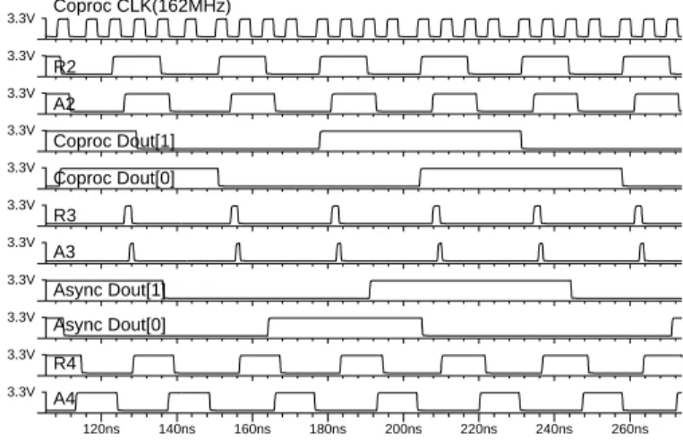
We performed extensive SPICE simulations of the chip after backannotating the layout parasitics into the schematic, using Mentor Graphics Accusim. The timing trace in Fig. 10 shows a simulation result including handshake and data signals. CPU andCoproc are programmed to run at 327MHz and 162MHz respectively in this case. The frequencies ofR2andA2 (hand-shake signals betweenCoprocandAsync) are one fourth that of Coprocclock, because it takes one clock cycle to sampleA2and another clock cycle to toggleR2. R2 andA2 have about 50%
120ns 140ns 160ns 180ns 200ns 220ns 240ns 260ns 3.3V 3.3V 3.3V 3.3V 3.3V 3.3V 3.3V 3.3V 3.3V 3.3V 3.3V A4 R4 Async Dout[0] Async Dout[1] A3 R3 Coproc Dout[0] Coproc Dout[1] A2 R2 Coproc CLK(162MHz)
Fig. 10. Simulation trace (fCoproc= 162 MHz,fCPU= 327 MHz).
Fig. 11. Die photo.
duty cycle because they are “synchronized” to Coproc clock; however,R3andA3have much narrower pulses becauseFIFO2 (output side ofAsync) is never full and thus responds quickly.
The chip (die photo shown in Fig. 11) was fabricated in 0.5µm HP CMOS14TB triple-metal process through MOSIS. Our test results show that the fabricated chips function correctly, but test results are found to be much faster than the simulated re-sults (with a scale factor of 1.4). We believe that this is due, in part, to the conservative estimation of parasitics by the Mentor tool.
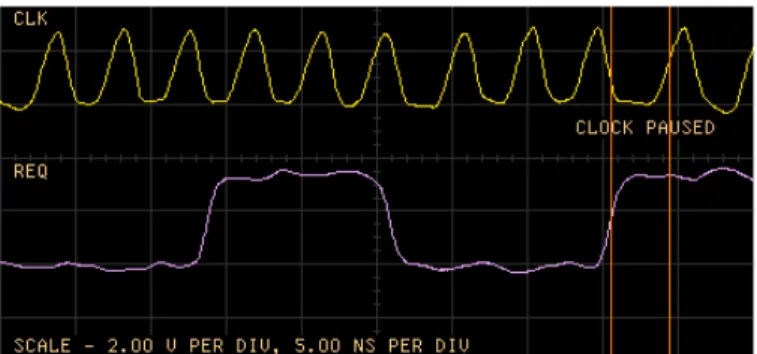
Test results clearly indicate that the clocks do become stretched. Although we were not able to observe high fre-quency clock signals (due to the pad design limitations),4 we
could clearly observe several instances of clock pausing when the CPU module was programmed to operate at 162MHz (simu-lation speed). An oscilloscope trace is shown in Fig. 12. Signals labeledCLKandREQaresysclkandRρof theCPUmodule ob-served at the pins of the fabricated chip.CLKis paused ifREQ toggles within the window of vulnerability ofCLK+, which was calculated to be between −3.43ns and−2.43ns from the ris-ing edge ofCLK(with a scale factor of 1.4 taken into account). However, the time difference betweenCLKandREQobserved on the oscilloscope as shown in Fig. 12 is outside the calculated window. In fact, the instance captured in Fig. 12 shows that CLKpauses even whenREQrises 3.85ns beforeCLKrises. The source of this discrepancy is unclear. We conjecture that not all delays scale the same. Test measurements were made with HP 54720A Oscilloscope with two 4 GSa/s plug-in cards.
Table I compares the nominal frequencies (without clock
4We used pads readily available from MOSIS which could not support the high speed clock signals.
Test Simulation No. of Fraction of Operating Nominal Operating Handshake Input Clock Cycle Stretched
(without pause) (with pause) Transitions Per H/S Transition
CPU Coproc CPU Coproc CPU Coproc Per 1000ns CPU Coproc
(456MHz) (456MHz) 327MHz 327MHz 290MHz 290MHz 148 0.25 0.25
(456MHz) 236MHz 327MHz 162MHz 290MHz 150MHz 152 0.24 0.08
236MHz (456MHz) 162MHz 327MHz 150MHz 290MHz 128 0.09 0.29
236MHz 236MHz 162MHz 162MHz 150MHz 150MHz 124 0.10 0.10
TABLE I
COMPARISON OF NOMINAL AND OPERATING FREQUENCIES(3.3V,27◦C, N68MARRUN).
Fig. 12. Oscilloscope trace illustrating clock stretching (sysclkfrequency = 236 MHz tested at 3.3V and22◦C).
pausing) and the operating frequencies obtained from simula-tion and test. The number shown in parentheses (456MHz) was obtained by extrapolation, not from the actual test. This is due to the limitation imposed by I/O pads. However, all the data and handshake signals, measurable because of their low frequencies, have been tested to be correct, even when the clock is set to the maximum frequency. Thus we concluded that the clock internal to the chip does not result in any synchronization failures. We extrapolated the top clock speed from the simulation and lower-speed clock signals measured from the test.
The impact of clock pausing on performance can be deduced from Table I. For example, when the nominal frequencies of CPUandCoprocare programmed to be 327MHz and 162MHz, the actual operating frequencies are 290MHz and 150MHz re-spectively (according to simulation). Therefore, CPU clock is stretched 37 (nominal) clock cycles per 1000ns and Coproc clock 12 cycles per 1000ns. However, clock stretching poten-tially occurs only when handshake inputs toggle. We measured 152 handshake input transitions per 1000ns for this case. Thus, in this case, the fraction of clock cycle stretched per handshake input transition forCPU is 15237 = 0.24. As the frequency is lowered, the number of clock cycles stretched becomes smaller. This is because the “window of vulnerability” as a fraction of a clock period becomes smaller.
Clearly, we are trading off system performance for commu-nication reliability and latency. In fact, the degradation inCPU throughput is about 12% in this configuration. However, we as-sert that we can gain back this loss and possibly more by oper-ating the system at a higher speed, i.e., by tuning the ring oscil-lator to a higher frequency. Systems with a ring osciloscil-lator clock do not require as much margin for the worst-case design as the ones with a fixed reference clock, because the operating condi-tion changes affect both the logic and ring oscillators similarly.
VI. CONCLUSION
We presented a new communication strategy, which is based on the pausible clocking scheme, for multiple synchronous mod-ules operating independently. We described the design and im-plementation of the pausible clock unit in detail. In order to prove its feasibility, we implemented a 0.5µm CMOS chip, mimicking a heterogeneous ring. Our test results show that the chip functions correctly as simulated, up to the top clock speed of 456MHz. We suggested possible system configurations (het-erogeneous rings and bus based systems) and practical limita-tions. We also determined analytical performance bounds and analyzed the effects of clock stretching on overall system per-formance.
Acknowledgment
The authors would like to thank Ryan Donohue, Reza Jalilizeinali, and LiJen Ko for their chip design effort.
REFERENCES
[1] M. J. Stucki and J. R. Cox Jr., “Synchronization strategies,” in Proceedings of the First Caltech Conference on Very Large Scale Integration, C. L. Seitz, Ed., 1979, pp. 375–393.
[2] C. L. Seitz, “System timing,” in Introduction to VLSI Systems, C. A. Mead and L. A. Conway, Eds., chapter 7. Addison-Wesley, 1980.
[3] D. M. Chapiro, Globally-Asynchronous Locally-Synchronous Systems, Ph.D. thesis, Stanford University, Oct. 1984.
[4] F. U. Rosenberger, C. E. Molnar, T. J. Chaney, and T. Fang, “Q-modules: Internally clocked delay-insensitive modules,” IEEE Transactions on Computers, vol. C-37, no. 9, pp. 1005–1018, Sept. 1988.
[5] J. N. Seizovic, “Pipeline synchronization,” in Proc. International Sympo-sium on Advanced Research in Asynchronous Circuits and Systems, Nov. 1994, pp. 87–96.
[6] L. F. G. Sarmenta, G. A. Pratt, and S. A. Ward, “Rational clocking,” in Proc. International Conf. Computer Design (ICCD), Oct. 1995, pp. 271– 278.
[7] M. R. Greenstreet, “Implementing a STARI chip,” in Proc. International Conf. Computer Design (ICCD), 1995, pp. 38–43.
[8] C. L. Seitz, “Ideas about arbiters,” Lambda, vol. 1, no. 1, First Quarter, pp. 10–14, 1980.
[9] Steven M. Nowick, Automatic Synthesis of Burst-Mode Asynchronous Controllers, Ph.D. thesis, Stanford University, Department of Computer Science, 1993.
[10] K. Y. Yun and D. L. Dill, “Automatic synthesis of extended burst-mode circuits: part II (automatic synthesis),” IEEE Transactions on Computer-Aided Design, vol. 18, no. 2, pp. 118–132, Feb. 1999.
[11] A. J. Martin, “On Seitz’s arbiter,” Tech. Rep. 5212:TR:86, Caltech Com-puter Science, 1986.
[12] T. Sakurai, “Optimization of CMOS arbiter and synchronizer circuits with submicron MOSFETs,” IEEE Journal of Solid-State Circuits, vol. 23, no. 4, pp. 901–906, Aug. 1988.
[13] M. B. Josephs and J. T. Yantchev, “CMOS design of the tree arbiter el-ement,” IEEE Transactions on VLSI Systems, vol. 4, no. 4, pp. 472–476, Dec. 1996.
[14] IEEE Standard 1596-1992, “Scalable coherent interface (SCI),” 1992. [15] S. B. Furber and P. Day, “Four-phase micropipeline latch control circuits,”