1. General
description
The TDA18275 is a high performance silicon tuner designed for terrestrial and cable TV
reception for both analog and digital broadcasts.
The TDA18275 supports all analog and digital TV standards and delivers a Low IF (LIF)
signal to a demodulator for analog TV and/or a channel demodulator for digital TV.
The TDA18275 facilitates TV design by:
•
Allowing on-board integration
•
Drastically reducing the tuner Bill Of Material (BOM)
•
Providing flexibility in system solution development
2. Features and benefits
Single 3.3 V supply voltage
Worldwide multistandard terrestrial and cable capabilities
Alignment free
RoHS compliant
I
2C-bus interface compatible with 3.3 V microcontrollers
Fully integrated oscillators
Fully integrated RF selectivity (no need for RF tracking filters coils)
2 programmable General-Purpose Outputs (GPO)
Dual IF output ports
1.7 MHz, 6 MHz, 7 MHz, 8 MHz and 10 MHz channel bandwidths
LIF channel center frequency output ranging from 0.8 MHz to 7.5 MHz
Fully integrated IF selectivity; eliminating the need for external SAW filters
Large flexibility in the IF filtering stage to ease the matching with various demodulators
circuits
Single-ended RF input, no need for external balun
Excellent return loss compatible with cable requirements
Power Level Detector (PLD) embedded
Integrated gain control
Self-AGC synchronization mode (VSync) for analog reception
Very fast tuning time
Strong immunity to LTE interferers in the digital dividend bandwidth
Strong immunity to WLAN interferers (802.11 a/b/g/n)
cable TV reception
3. Quick reference data
[1] Test scenario: standard NTSC M/N.
4. Ordering
information
Table 1.
Quick reference data
Symbol Parameter
Conditions
Min
Typ
Max
Unit
f
RFRF frequency
full range of RF input
42
-
1002
MHz
NF
tuntuner noise figure
75
impedance source;
maximum gain;
RF < 870 MHz
-
3.3
3.8
dB
75
impedance source;
maximum gain;
870 MHz
RF
1002 MHz
-
3.9
4.5
dB
jitphase jitter
integrated from 250 Hz to
4 MHz
-
0.4
0.6
degree
imageimage rejection
worst case, measured at
4 MHz IF frequency and for
image levels above
60 dB
V
-
65
-
dB
CSO
composite
second-order distortion
worst interferer over RF
frequency with respect to
wanted carrier
[1]
-
70
65
dBc
CTB
composite triple beat
-
70
65
dBc
ICP
1dB1 dB input
compression point
at the tuner input and
minimum gain
120
-
-
dB
V
Table 2.
Ordering information
Type number
Package
Name
Description
Version
TDA18275HN/C1 HVQFN32
plastic thermal enhanced very thin quad flat
package; no leads; 32 terminals; body
5
5
0.85 mm
TDA18275_SDS All information provided in this document is subject to legal disclaimers. © NXP B.V. 2013. All rights reserved.
Product short data sheet Rev. 2 — 14 October 2013 3 of 8
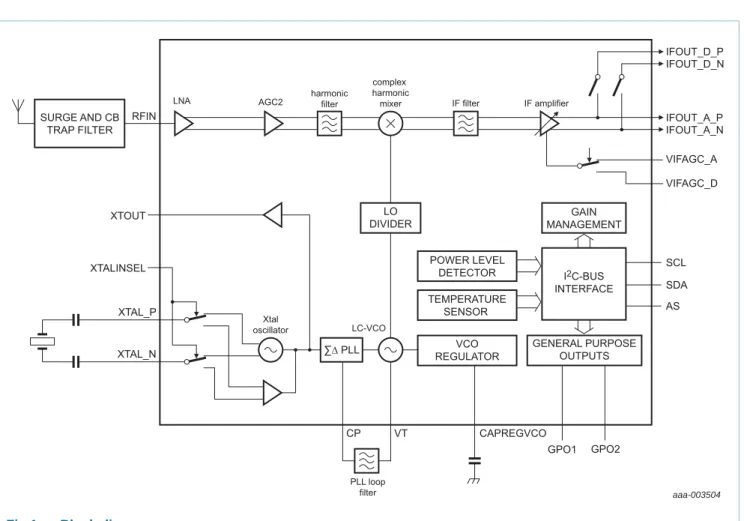
5. Block
diagram
Fig 1.
Block diagram
SURGE AND CB TRAP FILTER RFIN
XTALINSEL XTOUT XTAL_P XTAL_N ∑∆ PLL LO DIVIDER VCO REGULATOR LC-VCO Xtal oscillator harmonic filter AGC2 complex harmonic
mixer IF filter IF amplifier
CP VT IFOUT_A_P IFOUT_A_N IFOUT_D_P IFOUT_D_N VIFAGC_A VIFAGC_D CAPREGVCO PLL loop filter I2C-BUS INTERFACE GENERAL PURPOSE OUTPUTS GAIN MANAGEMENT POWER LEVEL DETECTOR TEMPERATURE SENSOR SDA SCL AS GPO2 LNA GPO1 aaa-003504
6. Limiting
values
[1] The maximum allowed ambient temperature Tamb(max) depends on the assembly conditions of the package and especially on the design of the Printed-Circuit Board (PCB) and die connection. The application mounting must be done in such a way that the maximum junction temperature is never exceeded. The junction temperature can be obtained by reading the temperature sensor bit via I2C-bus. The junction temperature: Tj = Tamb + Tj-c. where Tj-c = powerRth.
[2] Class IV: 1000 V.
Table 3.
Limiting values
In accordance with the Absolute Maximum Rating System (IEC 60134).
Symbol Parameter
Conditions
Min
Max
Unit
V
CCsupply voltage
0.3
+3.6
V
V
Iinput voltage
V
CC< 3.3 V
0.3
V
CC+ 0.3 V
V
CC> 3.3 V
0.3
+3.6
V
T
stgstorage temperature
40
+150
C
T
jjunction temperature
-
150
C
T
ambambient temperature
20
[1]
C
V
ESDelectrostatic discharge voltage
EIA/JESD22-A114 (HBM)
2
+2
kV
EIA/JESD22-C101-C (FCDM) class III
[2]1000
-
V
GPO pins: GPO1 and GPO2
V
CCsupply voltage
0 V < V
pu< 5.5 V; R
pu> 390
0.3
+5.5
V
I
CCsupply current
corresponding GPO ON
20
0
mA
V
ESDelectrostatic discharge voltage
EIA/JESD22-A114 (HBM)
650
+650
V
TDA18275_SDS All information provided in this document is subject to legal disclaimers. © NXP B.V. 2013. All rights reserved.
Product short data sheet Rev. 2 — 14 October 2013 5 of 8
7. Abbreviations
8. Revision
history
Table 4.
Abbreviations
Acronym
Description
AGC
Automatic Gain Control
AS
Address Selection
BOM
Bill Of Material
CB
Citizen Band
ESD
ElectroStatic Discharge
FCDM
Field-induced Charged-Device Model
GPO
General Purpose Outputs
HBM
Human Body Model
IF
Intermediate Frequency
LC-VCO
Inductors and Capacitors - Voltage Controlled Oscillator
LIF
Low IF
LNA
Low-Noise Amplifier
LO
Local Oscillator
LTE
Long-Term Evolution
NF
Noise Figure
NTSC
National Television System Committee
PCB
Printed-Circuit Board
PLD
Power Level Detector
PLL
Phase-Locked Loop
RF
Radio Frequency
RoHS
Restriction of Hazardous Substances
SAW
Surface Acoustic Wave
VCO
Voltage Controlled Oscillator
VSync
Vertical Synchronization
Xtal
Crystal
WLAN
Wireless Local Area Network
Table 5.
Revision history
Document ID
Release date
Data sheet status
Change notice
Supersedes
TDA18275_SDS v.2
20131014
Product short data sheet
-
TDA18275_SDS v.1
Modifications:
•
Table 1
: updated.
-9. Legal
information
9.1 Data
sheet
status
[1] Please consult the most recently issued document before initiating or completing a design. [2] The term ‘short data sheet’ is explained in section “Definitions”.
[3] The product status of device(s) described in this document may have changed since this document was published and may differ in case of multiple devices. The latest product status information is available on the Internet at URLhttp://www.nxp.com.
9.2 Definitions
Draft — The document is a draft version only. The content is still under internal review and subject to formal approval, which may result in modifications or additions. NXP Semiconductors does not give any representations or warranties as to the accuracy or completeness of information included herein and shall have no liability for the consequences of use of such information.
Short data sheet — A short data sheet is an extract from a full data sheet with the same product type number(s) and title. A short data sheet is intended for quick reference only and should not be relied upon to contain detailed and full information. For detailed and full information see the relevant full data sheet, which is available on request via the local NXP Semiconductors sales office. In case of any inconsistency or conflict with the short data sheet, the full data sheet shall prevail.
Product specification — The information and data provided in a Product data sheet shall define the specification of the product as agreed between NXP Semiconductors and its customer, unless NXP Semiconductors and customer have explicitly agreed otherwise in writing. In no event however, shall an agreement be valid in which the NXP Semiconductors product is deemed to offer functions and qualities beyond those described in the Product data sheet.
9.3 Disclaimers
Limited warranty and liability — Information in this document is believed to be accurate and reliable. However, NXP Semiconductors does not give any representations or warranties, expressed or implied, as to the accuracy or completeness of such information and shall have no liability for the consequences of use of such information. NXP Semiconductors takes no responsibility for the content in this document if provided by an information source outside of NXP Semiconductors.
In no event shall NXP Semiconductors be liable for any indirect, incidental, punitive, special or consequential damages (including - without limitation - lost profits, lost savings, business interruption, costs related to the removal or replacement of any products or rework charges) whether or not such damages are based on tort (including negligence), warranty, breach of contract or any other legal theory.
Notwithstanding any damages that customer might incur for any reason whatsoever, NXP Semiconductors’ aggregate and cumulative liability towards customer for the products described herein shall be limited in accordance with the Terms and conditions of commercial sale of NXP Semiconductors.
Suitability for use — NXP Semiconductors products are not designed, authorized or warranted to be suitable for use in life support, life-critical or safety-critical systems or equipment, nor in applications where failure or malfunction of an NXP Semiconductors product can reasonably be expected to result in personal injury, death or severe property or environmental damage. NXP Semiconductors and its suppliers accept no liability for inclusion and/or use of NXP Semiconductors products in such equipment or applications and therefore such inclusion and/or use is at the customer’s own risk.
Applications — Applications that are described herein for any of these products are for illustrative purposes only. NXP Semiconductors makes no representation or warranty that such applications will be suitable for the specified use without further testing or modification.
Customers are responsible for the design and operation of their applications and products using NXP Semiconductors products, and NXP Semiconductors accepts no liability for any assistance with applications or customer product design. It is customer’s sole responsibility to determine whether the NXP Semiconductors product is suitable and fit for the customer’s applications and products planned, as well as for the planned application and use of customer’s third party customer(s). Customers should provide appropriate design and operating safeguards to minimize the risks associated with their applications and products.
NXP Semiconductors does not accept any liability related to any default, damage, costs or problem which is based on any weakness or default in the customer’s applications or products, or the application or use by customer’s third party customer(s). Customer is responsible for doing all necessary testing for the customer’s applications and products using NXP
Semiconductors products in order to avoid a default of the applications and the products or of the application or use by customer’s third party customer(s). NXP does not accept any liability in this respect.
Limiting values — Stress above one or more limiting values (as defined in the Absolute Maximum Ratings System of IEC 60134) will cause permanent damage to the device. Limiting values are stress ratings only and (proper) operation of the device at these or any other conditions above those given in the Recommended operating conditions section (if present) or the Characteristics sections of this document is not warranted. Constant or repeated exposure to limiting values will permanently and irreversibly affect the quality and reliability of the device.
Terms and conditions of commercial sale — NXP Semiconductors
products are sold subject to the general terms and conditions of commercial sale, as published at http://www.nxp.com/profile/terms, unless otherwise agreed in a valid written individual agreement. In case an individual agreement is concluded only the terms and conditions of the respective
Document status[1][2] Product status[3] Definition
Objective [short] data sheet Development This document contains data from the objective specification for product development. Preliminary [short] data sheet Qualification This document contains data from the preliminary specification.
TDA18275_SDS All information provided in this document is subject to legal disclaimers. © NXP B.V. 2013. All rights reserved.
Product short data sheet Rev. 2 — 14 October 2013 7 of 8
Export control — This document as well as the item(s) described herein may be subject to export control regulations. Export might require a prior authorization from competent authorities.
Quick reference data — The Quick reference data is an extract of the product data given in the Limiting values and Characteristics sections of this document, and as such is not complete, exhaustive or legally binding. Non-automotive qualified products — Unless this data sheet expressly states that this specific NXP Semiconductors product is automotive qualified, the product is not suitable for automotive use. It is neither qualified nor tested in accordance with automotive testing or application requirements. NXP Semiconductors accepts no liability for inclusion and/or use of
non-automotive qualified products in automotive equipment or applications. In the event that customer uses the product for design-in and use in automotive applications to automotive specifications and standards, customer (a) shall use the product without NXP Semiconductors’ warranty of the product for such automotive applications, use and specifications, and (b) whenever customer uses the product for automotive applications beyond NXP Semiconductors’ specifications such use shall be solely at customer’s own risk, and (c) customer fully indemnifies NXP Semiconductors for any liability, damages or failed product claims resulting from customer design and use of the product for automotive applications beyond NXP Semiconductors’ standard warranty and NXP Semiconductors’ product specifications.
Translations — A non-English (translated) version of a document is for reference only. The English version shall prevail in case of any discrepancy between the translated and English versions.
9.4 Licenses
9.5 Trademarks
Notice: All referenced brands, product names, service names and trademarks are the property of their respective owners.
I2C-bus — logo is a trademark of NXP B.V.
10. Contact information
For more information, please visit:
http://www.nxp.com
For sales office addresses, please send an email to:
ICs with DVB-T or DVB-T2 functionality
Use of this product in any manner that complies with the DVB-T or the DVB-T2 standard may require licenses under applicable patents of the DVB-T respectively the DVB-T2 patent portfolio, which license is available from Sisvel S.p.A., Via Sestriere 100, 10060 None (TO), Italy, and under applicable patents of other parties.
11. Contents
1
General description . . . 1
2
Features and benefits . . . 1
3
Quick reference data . . . 2
4
Ordering information . . . 2
5
Block diagram . . . 3
6
Limiting values. . . 4
7
Abbreviations . . . 5
8
Revision history . . . 5
9
Legal information. . . 6
9.1
Data sheet status . . . 6
9.2
Definitions . . . 6
9.3
Disclaimers . . . 6
9.4
Licenses . . . 7
9.5
Trademarks. . . 7
10
Contact information. . . 7
11
Contents . . . 8