12
Storage Technology
Figure 12.1. GE’s holographic storage hardware, http://ge.geglobalresearch.com/ blog/breakthrough-in-micro-holographic-data-storage
S
toragetechnology continues to advance, both in terms of capacity andperfor-mance. For example, Hitachi’s new Ultrastar He6 hard drives store 6TB on
seven drive platters in a helium-filled enclosure1. Although hard drives offer
an attractive storage–cost ratio, newer alternatives like optical discs and flash memory are now common. Research in areas like holographic storage, molecular memory, and magnetoresistive memory point to potential future technology that may offer signifi-cant advantages in storage capabilities.
12.1
Optical Drives
Storage on optical drives like CDs, DVDs, and Blu-ray discs are based on phase change recording, which uses a laser to alter the crystalline structure of a
record-1http://www.hgst.com/hard-drives/enterprise-hard-drives/enterprise-sas-drives/
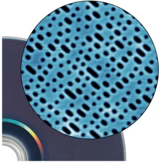
Figure 12.2. An atomic force microscope image of a Blu-ray disc surface magnified 20,000×, showing pits in black and lands in blue
ing media. This affects how light is reflected or absorbed when illuminated, allowing us to create a sequence of 0s or 1s on a disc’s surface.
12.1.1 Compact Discs
Compact discs (CDs) were developed independently, then jointly by Philips and Sony. The first CD format and CD players were introduced in 1982. CDs are an optical system, with no read–write head. Instead, a laser source is focused and positioned via a lens onto the surface of the CD, which reflects the light back to a sensor for interpretation. Data on a CD is made up of tiny indentations, orpits, that follow a spiral track over the surface of the disc.
The data layer of the CD is covered by a 1.2mm plastic substrate. This protects the disc, and since the laser is unfocused at its surface, it helps it to ignore surface dust and fingerprints. This rugged functionality is one key reason why CDs evolved into a mass market removable–transportable media.
Commercial CDs are produced using a mold of a CD’s pits, and a high speed du-plication machine to stamp out copies. CD-Rs and CD-RWs allow users to write data directly. This is done by coating the surface of the disc with a phase-change material. The surface can exist in two stable states: crystalline, with the atoms arranged in a regular 3D lattice, and amorphous, with the atoms arranged in a random pattern. If the surface is heated to a few hundred degrees C, the atoms rearrange into the crys-talline phase. If the surface is heated to> 600◦C, a melting point is achieved, and the amorphous phase results. By rapidly cooling the surface, the atoms don’t have an
12.1. Optical Drives
opportunity to jump back to the crystalline state. The laser is placed in a high power mode to produce amorphous marks, in a medium-power mode to “overwrite” a mark back to the crystalline state, and a low power mode to read the marks.
Speed.The original CD-ROM ran at 1.2Mb/s (125KB/s), rotating at 200–500 rpm
de-pending on whether the laser is positioned at the outer or inner track. This was the rate needed for audio playback. Computer-based CD-ROMs have increased rotation rates to increase the speed of data transfer. Above 12×CD-ROMs read at a constant
angu-lar velocity, so the motor does not need to change the speed of the drive as the laser is positioned to different tracks. For example, a 32×CD-ROM rotates at 4000 rpm,
reading data at about 38Mb/s on the outer track, and at about 16Mb/s (13×) on the
inner track.
Recording speeds are normally slower than reading speeds, because this depends on how quickly the recording material can change its phase. The original CD-RW drives ran at 1×, needing about 0.5ms for phase change. Modern CD-RWs run at up
to 12×recording speeds (15 Mb/s).
Audio CDs hold up to 74 minutes of sound in 333,000 sectors (2352 bytes/sector, divided into 24-byte frames), for a total capacity of 682MB. Computer-based CD-ROMs can hold up to 737MB of data on a standard CD.
12.1.2 Digital Versatile Disc
Digital Versatile Discs2(DVDs) followed CDs in 1995 for storing video. DVDs were invented in a collaboration between Philips, Sony, Toshiba, and Panasonic.
The original DVDs held 1.36GB of data, enough for about 135 minutes of standard definition (SD) video. The 1×transfer rate of a DVD is 11Mb/s, the rate needed to
support video playback. Faster drives and multi-sided, multi-layer discs have been introduced to increase both transfer rates and storage capacities. DVD players use a 650 nm red laser, as opposed to the 780 nm red laser used in a CD player. This produces a smaller spot, allowing smaller pits and more capacity on the disc.
Various recordable DVD formats were also introduced: DVD-RAM by Panasonic to hold up to 4.8GB of random access data, DVD-R/RW by Pioneer to hold up to 4.7GB of consumer video, and DVD+R/RW by Sony and Philips, also capable of holding up to 4.7GB of consumer video.
12.1.3 Blu-ray
Blu-ray discs (BD), developed to replace DVDs, are designed to hold high definition (HD) video. Blu-ray players use a 405 nm blue laser diode. This was a major technical achievement, made by Sony and Philips in the late 1990s. Other important advances were also required, for example, a very hard and thin polymer used to protect the surface of consumer BDs.
Initially, two HD video recording standards existed: Blu-ray and HD-DVD, posed by Toshiba and NEC. The key for both standards was convincing movie pro-duction studios to release movies in their format. Initially, HD-DVD was supported 2DVD initially meant Digital Videodisk, but that was changed to Digital Versatile Disc to emphasize a DVD’s ability to store data other than video.
by Paramount, Warner Brothers, and Universal. Blu-ray was supported by Columbia, Walt Disney, and 20th Century Fox. These alliances shifted until January 2008 when Warner Brothers, the only remaining distributor of HD-DVDs, announced their movies would be released in Blu-ray. This effectively killed the HD-DVD format as major US retail chains like Walmart dropped HD-DVD discs from their stores.
The first BD-ROM players were introduced in mid-2006. Sony’s PS3 video game console, introduced in Japan and the United States in November 2006, included a Blu-ray player as standard equipment. This significantly constrained the initial pro-duction of PS3s, because of a shortage of blue laser diodes. Sony’s strategy was to entrench Blu-ray as the new standard for HD video distribution by generating a large market share of players through sales of PS3s, a strategy that was eventually success-ful. Based on North American PS3 sales (27.3 million3) versus the estimated number
of US households that purchased Blu-ray players (61 million4), approximately 45%
of Blu-ray players sold are PS3s.
Standard BDs hold 25GB of data. Dual layer discs hold 50GB. A 1×BD transfers
data at about 36Mb/s. Drives currently run up to 16×, or about 576 Mb/s (72 MB/s).
Recordable and re-writable variations of Blu-ray—BD-R and BD-RE, respectively– are available. Initially these formats were designed to hold video data, but they have been updated to use UDF as their file system, supporting more general data storage.
12.2
Solid State Drives
Solid state drives (SSDs) are data storage devices that use either DRAM or non-volatile NAND flash memory to store information. SSDs are already the default storage device on smartphones, tables, and cameras, and are now available on most laptops. Although less common, they are also used in desktop computers and stor-age arrays. Examples include USB keys, SDHC memory cards, and larger capacity storage arrays packaged in hard drive form factors.
DRAM-based SSDs use the same type of memory as that used in PCs and graphics cards. It offers very fast access times, on the order of 0.01ms. Because DRAM is volatile, the drives require batteries or external power, plus a backup storage space like a traditional hard drive to copy the contents from DRAM when power is removed, then back into memory when power is restored. This is similar to hibernation sleep mode on a PC.
For flash-based SSDs, the memory is a type of EEPROM—electronically erasable-programmable read only memory. Flash memory was invented by Fujio Masuoka at Toshiba in 1980. The term “flash” was used because the block erase operation is reminiscent of a camera flash.
12.2.1 Floating Gate Transistors
Physically, flash memory is a large collection of floating gate transistors. Unlike tra-ditional transistors, floating gate transistors are non-volatile. They can maintain their
3http://www.vgchartz.com/analysis/platform_totals/
4
12.2. Solid State Drives
Figure 12.3.A block diagram of a floating gate transistor
state without the need for an external charge by creating a floating gatecage, then us-ing quantum tunnelus-ing to migrate electrons into or out of the cage5. Electrons trapped
in the cage remain trapped regardless of whether power is applied, forming a binary 1 if the cell is uncharged, or a 0 if it’s charged.
Floating gate transistors come in SLC—single-level cell—and MLC—multi-level cell—forms. SLC transistors have a single charge level, representing a 1—no charge— or a 0—charged. MLC transistors support multiple charge levels. For example, a 4-level MLC transistor supports four values: 11—no charge—and 10, 01, and 00— three different and distinguishable levels of charge. SLC cells are more reliable and faster, but cost more for a given amount of storage. MLC cells are cheaper, allowing increased storage density, but at the cost of potential reliability. Regardless, almost all consumer-level SSDs use MLC transistors.
Floating gate transistors have three connections: gate, source, and drain (Fig. 12.3). The floating gate sits between the gate connector and the rest of the transistor. If the floating gate has no charge, a small voltage applied to the gate closes the transistor and allows it to conduct current from source to drain. If the gate contains a charge, a larger voltage is required to allow current to flow.
A NAND flash block is made up of a grid of floating gate transistors. Each row of transistors represents apageof memory, wired together with aword linethat connects to the transistors’ gates. The sources and drains of each column of transistors are also connected in series with asource lineat the top and abit lineat the bottom. Voltages applied to the word lines, together with current applied to the transistors’ source lines and measured at their bit lines allow us to read a single transistor’s state. If current is reported at the drain, then the transistor has no charge in its floating gate, representing a bit value of 1.
NAND blocks have between 32 to 256 rows (pages), and 4096 to 65536 columns, representing from 16KB to 2MB of memory. Typical page sizes are normally 8KB, which fits nicely with common OS cluster sizes of 4KB or 8KB.
5
12.2.2 Read–Write–Erase
NAND flash memory has a major implementation constraint: data can only be read and written one page at a time. So, to update a single byte in a page, NAND reads the page into a cache, changes the byte, then writes the page back out again.
This leads to another constraint on NAND flash memory. Data cannot be over-writtenin place. To write data, the NAND memory must be erased to an initial state of all 1s. Individual 1s can be converted to 0s—by adding charge to the transistor’s gate—but they cannot be selectively reset back to 1s. Since a high voltage is needed to erase a transistor, erase operations must be applied to an entire block.
One consequence of the overwriting and erasing constraints is that SSDs can po-tentially become slower over time. Initially, many empty pages exist to hold new data. Changing data can’t overwrite in place, however. Instead, the old version of the page is marked as inactive, and the new version is written to a different location. As free pages decrease, it may become necessary to read an entire block into cache, erase the block, consolidate the block’s active and inactive pages to make new free pages, then write it back. This read–erase–write cycle is slow, causing read operations to take more time to complete.
A third constraint on NAND memory is that it can only be written a finite number of times before it no longer functions correctly. During each block erase a very small amount of charge can become trapped in the dielectric layer that makes up the floating gate. Over time the buildup of this charge leads to a resistance that no longer allows the floating gate to change from 1 to 0. Current consumer-level SSDs allow on the order of thousands of writes.
12.2.3 SSD Controller
SSD controllers perform data striping and error correction to improve performance and guard against data corruption. They also perform a number of operations to ad-dress the issues of overwriting, block erasing, and write degradation.
First, many drives are over-provisioned to hold more memory than their stated capacity. This makes free pages available, even when the drive is nearly full.
Second, the controller is constantly performing garbage collection to keep the SSD responsive. The SSD will locate blocks with inactive pages, copy the block’s active pages to new locations, then erase the entire block. This is done in the background, to try to ensure that free pages are available when needed, allowing us to avoid a costly read–erase–write cycle when data is actually being written. Modern OS’s use TRIM commands to inform an SSD to mark a file’s pages as inactive when the file is deleted, allowing them to be included during garbage collection.
Third, SSDs perform wear leveling to ensure that writes are distributed fairly evenly to all the blocks in the drive. The controller tracks how many writes each block receives, allowing it to distribute write requests throughout the drive, and to rotate static pages with active ones to ensure no blocks are underwritten.
Companies normally won’t reveal exactly how their drive controllers work, since this provides them with a certain amount of competitive advantage. For example, SandForce and EMC are said to use compression and block-level deduplication to
12.3. Holographic Storage
minimize the amount of incoming data that actually needs to be written to a drive. Details on how this works, and exactly how much performance improvement it pro-vides, are not available, however.
12.2.4 Advantages
SSDs offer a number of strengths and limitations. Advantages include
• low read latency, since there is no physical seek,
• fast start-up times, since there is no spin up of a disk platter, • high mechanical reliability, since there are no moving parts, and • silent operation.
SSDs also have a number of disadvantages. Currently, the two main constraints are cost, which is higher than HDDs, and maximum capacity, which is lower than HDDs. For example, a 512GB SSD sells for $300 to 600, or $0.59 to 1.17/GB. A 7200 rpm 1TB HDD sells for about $70, or $0.07/GB, more than 8×cheaper per GB
than the lowest cost SSD. There are also issues of asymmetric SSD read and write performance, and the potential for a limited useful lifetime.
12.3
Holographic Storage
Holographic storage, sometimes referred to as a 3D storage method, records data as variations in a reference laser beam. Although still in a research stage, the ability to store data holographically could significantly improve both capacity and transfer rates, based on the ability to split and modulate a laser beam in parallel.
12.3.1 Holograms
To understand holographic storage, you must first understand how holograms work. A hologram is a recording of an interference pattern made during the interaction of two beams of light. This is analogous to how ripples in a pond intersect and interact. Suppose two stones are dropped in a pond. The peaks and troughs in their ripple patterns combine to amplify—when two peaks or two troughs overlap—or cancel— when a peak and a trough overlap.
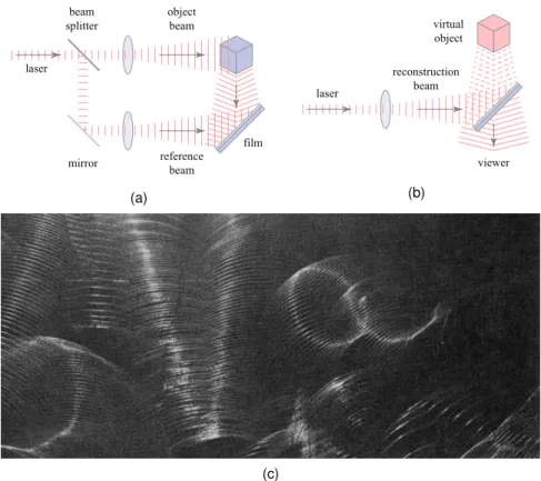
Light also travels in waves, with peaks and troughs that can interact with one another in a similar manner. This technique is exploited to create a hologram. In the basic setup, a recording film with very high resolution is struck simultaneously by two beams of light.
• Areference beamshot from a laser.
• Aobject beam, a light beam from the same laser reflected offan object’s surface.
The film records the interference pattern between the reference and object beams (Fig. 12.4a), producing a swirl of bright ridges and dark troughs (Fig. 12.4c). Laser light is used because it is stable and has coherence, both in wavelength and amplitude. To recreate the object, the same laser light, shot in the direction of the original reference beam, is passed through the hologram (Fig. 12.4b). The hologram reflects
beam splitter mirror laser object beam reference beam film reconstruction beam laser viewer virtual object (a) (b) (c)
Figure 12.4.Holograms: (a) capturing the interference patterns between a reference beam and an object beam; (b) striking the hologram with the reference beam to exttract the object beam and produce a hologram of the object; (c) a typical interference pattern
this beam in a way that “cancels out” the reference beam from the interference pattern, producing the original object beam, that is, the laser beam reflected offthe object’s surface. The viewer sees a reflected version of the object, floating in space. If the viewer moves their head, they see the object from different viewpoints, since reflected light from those perspectives has also been captured in the hologram.
12.3.2 Data Holograms
In holographic storage, the same object and reference beams are used to record infor-mation as an interference pattern. Here, the object beam does not reflect offa physical object. Instead, a spatial light modulator modifies the object beam based on data val-ues to be stored. By varying the reference beam’s wavelength and angle, and the position of interference on the recording media, several thousand different holograms can be stored on a single disc.
To read data, the original reference beam reflects offthe media. The reflected result is “reverse modulated” to extract the original data values that were stored. If the reference bean is diverged, the deflector can run in parallel, producing very fast
12.4. Molecular Memory
transfer rates. Various manufacturers have claimed storage of up to 500GB/in2and
transfer of an entire file of any size up to 500GB in 200ms. 12.3.3 Commercialization
InPhase Technologies was the first company to try to commercialize holographic stor-age through their Tapestry Media system, with anticipated capacities of 500GB to 6TB. InPhase filed for bankruptcy protection in October 2011. Their assets were ac-quired by Akonia Holographics, which launched as a company in August 2012.
Some of the holographic storage patents awarded to InPhase are jointly held with Nintendo of Japan. This has led to speculation that Nintendo may be the first company to introduce holographic storage for video games.
A competing technology is the Holographic Versatile Disc (HVD), initially de-veloped in 2004. HVD combines a pair of collimated green and red lasers, using the green laser to read holographic interference patterns at the surface of a disc, and the red laser to read tracking information on an aluminum layer at the bottom of the disk. To date, no companies have chosen to implement the HVD standard.
General Electric is also working on a holographic storage system that uses Blu-ray-sized discs. A system that can record 500GB discs was demonstrated in July 2011 (Fig. 12.1). GE’s micro-holographic storage material is said to record data at Blu-ray speeds, using technology similar to Blu-ray.
12.4
Molecular Memory
Molecular memory is an attempt to store and retrieve data at the molecular level, with the hope of significantly increasing storage density and therefore the overall capacity of a storage device. Molecular memory is non-volatile, so it can maintain its state without power, similar to magnetic storage or flash memory.
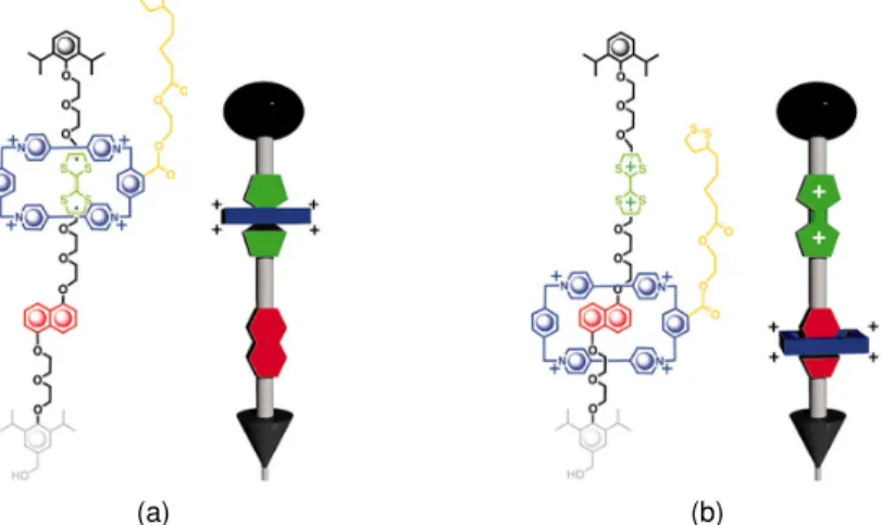
One example of the “molecular switches” used in this memory is called rotaxane. It has a barbell shape, with a ring of atoms that can move between the two ends of the bar via a voltage charge (Fig. 12.5). The conductivity of the molecule changes depending on where the ring is stationed, allowing two distinct states to represent binary 0 and 1.
Prototype chips sandwich a layer of molecules between two layers of nanowires. Each nanowire layer runs perpendicular to the other, forming a grid that is used to deliver voltage differences to change the state of a molecule. Rotaxane molecules are sensitive to water: one end is attracted, and the other end is repelled. This allows researchers to arrange the molecules so they are all aligned in the same direction in a 1-molecule thick layer.
Semiconductor memory has capacities of about 1.8GB/in2. Molecular memory
has demonstrated capacities of 100GB/in2.
Much work remains in terms of ensuring high yields on the molecular layer, deter-mining how to maintain the longevity of the molecules, optimizing access times, and so on. This molecular design is also being studied for semiconductors, which would allow manufacturers to replace silicon transistors with molecular transistors.
(a) (b)
Figure 12.5.Bi-stable rotaxane, with the atom ring over the positive and negative endpoints of the barbell, figures from “Evaluation of synthetic and linear motor-molecule actuation energetics”,http://www.pnas.org/content/103/23/8583.figures-only
Other potential molecules are also being developed. For example, researchers at the University of Tokyo have built a molecule that changes its shape when struck by a single light beam. This design incorporates the parallel investigation of using light rather than electrical pulses to move information within a computer chip.
Work at NASA Ames has produced amultilevel molecular memory cellcapable of manipulating three bit states rather than one. This means each cell can hold one byte. A set of molecular wires is used to chemically reduce or oxidize (redox) the molecule to set its state. Resistance is measured on a nanowire at the cell’s location to read back its state. In this way a redox molecule acts like a chemical gate controlling the number of electrons it allows to pass along the wire.
12.5
MRAM
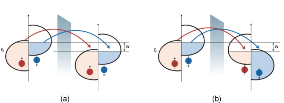
Magnetoresistive random access memory (MRAM) is a non-volatile memory technol-ogy that stores information using magnetic storage elements. A memory cell is made up of two ferromagnetic plates separated by an insulating layer. One plate has a fixed magnetic polarity. The other plate’s polarity can be changed. Normally, if both plates have the same polarity it represents bit 0, otherwise it represents bit 1 (Fig. 12.6). Resistance at the cell can detect these states.
The most advanced MRAM uses a process known as spin-torque transfer (STT) to change the free layer’s polarity. In STT, a stream of spin-aligned (polarized) electrons first pass through the fixed polarity layer, causing them to spin and become polarized in the fixed layer’s direction. When these spin-aligned electrons pass through the free polarity layer, they repolarize to that layer’s direction. During repolarization, the electrons spin and produce a torque that sends energy through the free polarity layer. With enough energy, the free layer’s polarity will reverse.
12.5. MRAM
(a) (b)
Figure 12.6.Spin-torque transfer: (a) when both layers have the same polarity, spin-aligned electrons pass more freely; (b) different polarity increases resistance, figures from “The emergence of spin electrons in data storage”, http://www.nature.com/nmat/journal/ v6/n11/pdf/nmat2024.pdf
STT allows the density of cells to approach 65nm, the minimum requirement for usable mass-market memory. MRAM is non-volatile and STT reduces the energy needed to write data. The belief is that MRAM can save up to 99% (or more) in power consumption. For reading, flash memory and MRAM have comparable power consumption. For writing, however, flash memory requires a very large voltage pulse to perform a block erase. This can also degrade the flash memory, limiting the number of write cycles it can support. MRAM has neither of these limitations.
Finally, MRAM access times have been shown to be as low as 10ns (nanoseconds) or less. For reference, 1ms=1,000,000ns, meaning we could perform 100 million memory accesses a second. Researchers suggest that, if production can be made cost efficient, MRAM could be used as a “universal” RAM, replacing all other existing types of memory storage.