INTERNAL DOCUMENT
85
O U T P U T M E M O R Y
A part of the electronic model for tides and stom surges
S. Ishiguro
1980
[This document should not be cited in a published bibliography, and is supplied for the use of the recipient only].
I N S T I T U T E O F O C E A I N I O G R A P H I C S C I E N C E S
INSTITUTE OF OCEANOGRAPHIC SCIENCES
Wormley, Godalming, Surrey, GU8 BUB.
(042-879-4141)
(Director: Dr. A . S. Laughton)
Bidston Observatory,
Birkenhead,
Merseyside, L43 7RA.
(051-652-2396)
(Assistant Director: Dr. D. E. Cartwright)
Crossway,
Taunton,
Somerset, T A 1 2DW.
(0823-86211)
INSTITUTE OF OCEANOGRAPHIC SCIENCES
INTERNAL DOCUMENT 85
O U T P U T M E M O R Y
A part of the electronic model for tides and storm surges
S. Ishiguro 1980
21 pages, 9 diagrams, 7 tables
Institute of Oceanographic Sciences, Wormley, Godalming,
CONTENTS
Abstract 2
1. Introduction 2
2. Scheme of the system 3
3. Circuit description 5
4. Physical arrangement 11
5. Adjustments and tests 15
6. Operation procedure 17
7. Performance 18
8. Conclusion 21
Acknowledgements 21
References 21
ABSTRACT
The output of each grid of the electronic model for tides and storm surges consists of three voltages which represent the water level, and the x and y components of water currents. Each voltage varies with time and contains data equivalent to typically IK words/sec. This rate is too high for most peripheral instruments in the system. A circuit block which interfaces between the grid and the peripheral instruments has been developed for this purpose. The block consists of a programmable scaling circuit, DAC, memory, ADC and timing circuit, and has an 8-bit resolution with a storage capacity enough for a 10-day storm surge. The block is assembled on a single board (20 x 16 cm'), and can be connected directly to the numerical printer, numerical-map printer, tape punch, XY recorder and vector printer in the model system.
1. INTRODUCTION
The electronic model for tides and storm surges contains its output data processing system which displays a set of output voltages from each grid of the model in usable forms; e.g. numerical tables, numerical maps, punched tapes, graphs and vector diagrams.
The speed of the data output from the grid is much faster than the maximum speeds of the peripheral display instruments. In order to adjust these speed differences, the data from the grid is first stored in a memory, then taken out at a speed matching each peripheral instrument. This memory is called 'Output Memory' in this system.
A 'Transient Recorder', the only .standard product available at the time of the planning of the system, had been used for the output memory until 1978. However, this was the only part of the system which limited the resolution of data to 6 bits, after the 'Input Memory' (Ref. 1) had been changed from 6 bits to 8 bits.
SCHEME OF THE SYSTEM
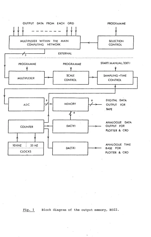
Fig. 1 shows the block diagram of the output memory.
A set of time varying voltages representing the x and y components of current (x, y), and water level (z) at each grid of the model is available simultaneously from the Main Computation Network (Ref. 4). These voltages are multiplexed by the multiplexer built in the network, so that a single set of voltages is selected at a time (typically
10 mill! seconds for a 10-day storm surge). The selection is carried out automatically by a programmed circuit, or manually.
A set of selected voltages consists of three voltages: x, y and z. One of them is again selected by a multiplexer within the system. The finally selected voltage is scaled by a scale control which is programmed in relation to the selection of grids in the model.
The timing and duration of sampling a selected voltage is carried out by the Sample-time Control. The timing of the start of sampling can be decided either manually or automatically by the START switch. In an automatic operation, a trigger is given at the start of each computation through the clock in the Input Memory (Ref. 1). The duration of sampling is normally fixed to the period of 255 clock pulses (typically about 26 ms) although the clock rate can be changed.
A sampled voltage is digitized by an 8-bit ADC, so that a set of 256 words data is obtained. This is written into a random access memory. When the writing of the memory is completed, the memory turns into a reading mode automatically, and produces the 256-word data repeatedly with the rate of 10k words/s. This digital output can be recorded, if necessary, by a magnetic recorder. In a normal operation, this output is displayed on a CRO through the DAC(Y), with a synchronized time base produced by the DAC(X).
Since the above mentioned memory-reading rate is too high for an XY plotter and tape punch, another reading rate, 25 words/s, has been prepared. The change of the reading rate is carried out by a manual switch, 'WRITE-PLOT'. When this switch is turned to the PLOT position, the read rate is still 10k words/s, but when the START switch is
pressed, the rate is changed into 25 words/s only for one set of reading (.256 words) , then automatically returns to the fast rate. During the slow reading, the outputs of the DAC(X) and DAC(Y) are fed into the XY plotter and tape punch, together with a signal for
OUTPUT DATA FROM EACH GRID PROGRAMME
EXTERNAL
STARTf M A N U A L / E X T ) PROGRAMME
PROGRAMME
DIGITAL DATA
OUTPUT FOR
TAPE
ANALOGUE DATA
OUTPUT FOR PLOTTER & CRO
ANALOGUE TIME BASE FOR PLOTTER & CRO COUNTER
DAC(X) DAC(Y)
10 KHZ
CLOCKS 25 HZ
SELECTION CONTROL
A D C
SCALE
CONTROL
MEMORY
MULTIPLEXER
SAMPLING-TIME
CONTROL MULTIPLEXER WITHIN THE M A I N
[image:6.596.49.542.51.823.2]COMPUTING NETWORK
3. CIRCUIT DESCRIPTIONS
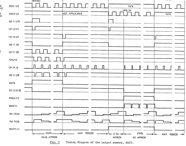
• Fig. 2 shows the circuit diagram of the output memory, and Fig. 3 shows its timing diagram.
Clocks
Two timers, 555(1) and 555(2), are used for the clocks of 10 kHz and 25 Hz respectively. An external clock input has been prepared for a more accurate clock rate in the input voltage sampling and for synchro-nization with the rest of the circuit in the model system. When the whole model is operated, the crystal clock in the Input Memory (Ref. 5) is used for the standard clock.
Normally the whole system is operated in a memory-read mode with the 10 kHz clock. Only when the WRITE-PLOT switch (SWl) is set to one of the positions, and START (SW2) or EXT TRIG is activated, the system turns into a memory-write mode or output-plot mode, both for a period of 256 clock pulses only. After this period, the system returns to a read mode automatically.
Read Mode
The 10 kHz clock generated by 555(1) enters into the chip-enable
terminal (CE) of the memory, 9112(1) and 9112(2), through 51/13, 51/4,
51/6 and 121(4)/6. The 121(4) is used for keeping the pulse width and shape constant independently from the type of clocks. During the read mode, the write/read terminals (WR) of the memory are kept high, and the switching terminal (SW) of 4066(1) and 4066(6) are kept low, by 04/6.
The shaped 10 kHz clock pulses from 121(4)/I enter into the binary code generator, 93(1) to 93(3), and its output (8-bit word) is fed into the address terminals of the memory. Therefore, the memory is read in the same order as its address numbers. The output from the 93(1) and
93(2) is converted into an analogue voltage by 2N425E(X) and 741(X) for
the time base of a CRO display. The output of the memory is also
con-verted into an analogue voltage by 2N425E(Y) and 741(Y) for the CRO
display.
Write Mode
A-7n
/2
LOKHI A N A
25Hz
P L O T - W R I T E 1
/
12V ion
lov ion
_
GD200 x 3 I 2 2 0 x 9
_ N 35 19 V
o , ^
X 34 .4 ^ 3
+ 15V
+15V -15V ]o/2 A A /\
5007(1)
10K//13K
741SC2)
+ 5 V
5 0 0 7 ( 2 )
lOKx 11 13
+ 15V -15V
ion
>
z
>z
w M
IN 4149( x 3 )
15,16
A D 5 7 0
MSB
9112(2) 9112(1) 4066 1 4 0 6 6 2
/
' ) > b n ') < t
11 i o o i o o o o
—4 > ^ 3:
•V N -D -0 X - < -0 X - < DrG OUT w
ANA OUT
Co
- S ) w
CLOCK 10 KHZ
CLOCK 25 HZ
START
CONV
DR &
WR
SW
RET
RLY
TAPE
X
Y
ZP
55511 1/3
555(2 J/3
00 11 ; / n
121 12)/1
121 (3;/1
00 11 )/6
121 (l )/6
5 7 0 / 1 7
121 U ] 6
00 [ 1 1/8
0 4 / 6
93 1 3 ) / 1 2
FYB51/C
SWl/11
741 IXV6
741 (Yj/6
RLY/7-lll
.n_n,
WRITEl a
i — ^
1
r
NOT APPLICABLE
n
n n n
j l h2567w.
1
I
ZL
ANY PERIOD
J " 1 r
PLOT
N / A
n n n n
•H n n J L
0 155 ->
l [ 3
[image:10.844.77.780.14.567.2]26mS APPROX APPROX
Fig. 3 Timing diagram of the output memory, BD22.
256Tp .
65 APPROX
READ
n n
N / A
I L J L i J 1
__r
The output pulses of 121(4)/I, which are the shaped pulse form of DR, enters into the binary code generator, 93(1) to 93(3). When 256 pulses have been entered, 93(3)312(RST') goes high, and resets the flip flop, 00(1)/6, through 121(3). Consequently, the analogue voltage fed into AD570/13 is digitized for a period which corresponds to 256 clock pulses
(the 10 kHz internal clock or an external clock with any frequency).
During the write mode, both the outputs of the binary code generator and the memory are converted into analogue voltages as in the read mode, so that they can be monitored by a CRO.
Plot Mode
The write mode is applied for both the XY plotter and tape recorder (either a tape punch or a magnetic tape recorder), since both a digital-data output with a timing signal and an analogue-digital-data output with an analogue time-base signal are available simultaneously. Because of the speed limitation of an XY plotter, the memory read rate of 25 words/s is used. This rate can be changed by adjusting the lOK VR connected to the 555(2) if necessary.
The plot mode is obtained by setting SWl to PLOT, and activated by START (SW2) manually. When this is activated, 121(2) generates a pulse of about 0.15 sec which is determined by the 22)j,F capacitor connected to 121(2)/II. Therefore, the flip flop, 00(1)/6 is set by this pulse, about 0.15 sec after SWl is activated. This delay is necessary for the movement of the XY plotter pen from the initial position to the start of a graph to be drawn. The initial position of the pen is determined by the data value written in the memory in the reset state, i.e. the data in its address No. 0. When SW2 is activated, the code generator is immediately reset. The flip flop, 00(1)/6 is also reset at the same time. Consequently, the data in the memory is read and plotted exactly in the same order as they were written.
The relay (in the bottom-right corner of Fig. 2) is activated through FYB51; only for the period which the 256 words in the memory are read, so that the analogue data output, analogue time-base and tape-recorder
command signal (one pulse for each word) are fed into the XY plotter and the tape punch (or recorder).
Multiplexers
Two groups of multiplexers are used for selecting one set of data voltages from each grid of the model (.three voltages from each grid;
e.g. 1500 voltages in all from 500 grids). The first group of
multi-plexers is built in the Main Computation Cabinet (see Fig. 1 for the
block diagram, and see Ref. 4 for their details). The second group of multiplexers is contained in this circuit, and used for selecting one of the three voltages (indicated by X, Y and Z at the board terminals
N 3 0 to N 3 5 in Fig. 2 ). Three sets of CMOS analogue switches, C D 2 0 0 S ,
are used for the second multiplexers which are controlled by a set of
10
Input-scale control
One of the voltages selected by the GD200S is passed through a
balanced input amplifier, 741S(1), and fed into the scaling circuit. The scaling circuit consists of two identical multiplying type DACs, 5007(1), 5007(2), and an operational amplifier, 741S(2), The 5007(1) amplifies an input signal consisting of an AC on a certain DC level, with 256 different gains depending on an 8-bit digital code fed into its terminals 5 to 12. The gain control of 5007(1) affects the DC level, as well as the AC signal. Tb compensate for this disadvantage, the 5007(2) controls the gain of a DC voltage in the same proportion as the DC level change in 5007(1), Consequently, the balanced output of 741s(2) has a controlled amplitude of AC signal with a constant DC level. This voltage is fed into AD570/13.
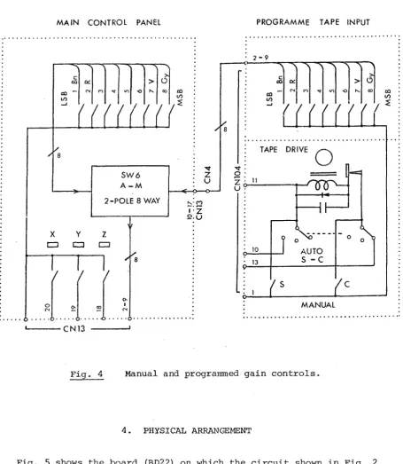
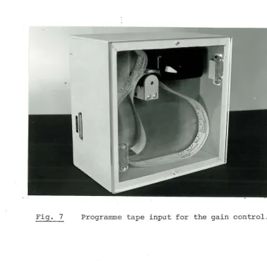
The gain control signal consists of 256 binary words (0 to 265 in a decimal equivalent), and is fed into board terminals Nl9 to N23. Fig. 4 shows two types of gain control:'Programme tape input' (in a separate case) and a set of 8 manual switches (on the main control panel) together with three voltage selection switches, X, y and Z. The former is used for a gain control which is synchronized with the selection of grids (see a separate paper for this necessity). The latter is used for individual control of gain.
The programme tape input is essentially a simple tape reader for a parallel 8-bit punched tape on which the control programme is recorded. The tape is driven by a step motor with synchronization of the scanning of grids of the model. The tape can also be moved continuously or step-by step, step-by controlling three switches, S, C and'AUTO S-C.
Bipolar/Monopolar Control
The dynamic range of AD570 can be used more efficiently by selec-ting its operation mode, either bipolar or monopolar according to the input-data voltage. This selection is carried out by controlling the voltage at terminals 15 of AD570, through BIP-MON switch (SW2) and 04/2. SW2 is on the main control panel.
Power Supply
11
M A I N CONTROL PANEL PROGRAMME TAPE INPUT
2 - 9
1 s - N "S •""S N
eg a: >
o
>
CO - CN r) •o CO
LO
A
-N "S s
\ \c
CO a: >
o
— •o
{ { ( ( { ( ( .
TAPE DRIVE
A - M
2-POLE 8 WAY
AUTO
MANUAL
•CN13
F i g . 4 M a n u a l a n d p r o g r a m m e d g a i n c o n t r o l s .
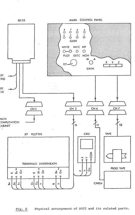
[image:13.597.63.519.73.597.2]4. PHYSICAL ARRANGEMENT
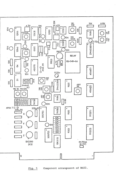
Fig. 5 shows the board (BD22) on which the circuit shown in Fig. 2 is arranged. BD22 is contained in the main control cabinet. Table 1 shows the connections of edge-connector terminals of BD22 and other circuits.
Fig. 6 shows the physical arrangement of BD22, the main control board (parts which are related to BD22 only), XY plotter, CRO, tape punch and programme-tape input for the gain control, together with their connectLors. Tables 1 to 4 show the circuit connection related to BD22.
Fig. 7 shows the actual apparatus of the programme-tape input for the gain control. This includes a tape driving system, and it is
1 2 § o S O o O o 4 7;%
o
(N§
o
ion oo
o
T07Z m IN4149VR4 IK VR310K^^
CO o O R in Q < V o ro
o o
CM OlfX CN CN u3
D ( ) LA" u3
rs (N SJ >U
(N CN (X o
ANA T O O 220^X6
I
1
220^X3 DG200 (X3) FBY51 RELAY RS-348-660
15 K 6-8K
] 1 = 1
[image:14.600.36.533.51.771.2]o
> -UJ (N z No
o
U1> S I ~o O § XT ry 5^ CM R IN 753A (6-3V) •13
BD22
EXT TRIG
EXT CLK
L
C N 5
L
M A I N
COMPUTATION CABINET
XY PLOTTER
M A I N CONTROL PANEL
8 7 6 5
O O O O
4 3 2 1
O O o o
G A I NWRITE INTC BiP
o - o o o
Y PLOT EXTC M O N
/ M A
/ ^ o
•
G A I NL
L
\
L
ACN 2
/ — 3
L
C N 4 CN 7
TERMINALS UNDERNEATH
q; m O
o O <j>
0)
CO
J C
d; ^ O
P <? o
CO O
V A .
L .>-V >-V
11
1
L
11
CRO TAPE
A
12
PROG TAPE
[image:15.602.51.500.46.759.2]CN104
14
Table 1. Connection of ED22 Output Memory
Table 2. Connection of CK2
P i n lio
R1 w CW15/9 SWl/11 W-PLOT 2 5 4 5 6 7 8 9 Gy V Be Gn Y Or E. Bn 15/27 25 CN14/20 19 18 17 16 15
8 MSB
7
DIG *
OUT 4
5 2 1 JLSB 10 11 12 15 Bn R Or Y CN2/1 2 5 4 XP
X P '
OUT
Z P '
14 15 16 Gy/R Be V BDll/2 CN2/5 6
TAPE COM'D
X Y
17-18 wu
19 20 21 22 25 24 25 26 En R Or Y Gy V Be Gn CN15/2 5 4 5 9 8 7 6 1 LSB 2
G A M 4
CCUT Q
7 6 5 27 26 29 W/R W/Be \j/Gn CN15/18 19 20 X
SEIEG Y
Z 50 51 52 55 54 55 Ba R Or Y Gn Be GB5/6 7 8 9 10 11
a X
Bk X '
m Y' R Z
Bk Z*
55 57 58 59 40 Gn Y Or R Bn CN15/26 27 28 10 REAR PAN BIP-MCN
E X T - I N T C
It START EXT TRIG C I 02 5 4 5 6 7 8 Bn R Or Y Gn Be V Gy CN15/1 2 5 4 5 6 7 8
W-PLOT SW
9-11 Gn Common
12 15-14 15 16 17 Bk R Gn Be 5V 15V Common -15V
Pin No
1 2 Bn R BD22/N10 11 PX PY
5 Or 12 PLT PZ
4 Y 15 PZ« 5
6 Be V
15 16 CRO
X Y
7--15 —
14 Gn Common
Table 5* Connection of CN4
Pin No
1 Gn Common
2 Bn GI415/10 1 LSB
5 R 11 2
4 Or 12 5
5 Y 15 4
6 Gn ^ ^ 1 4 5
7 Be m 6
8 V 16 7
9 Gy 17 8 MSB
10 Y CN5/4 5055 COL
11 Bn 24V
12 Gn Common
15-25
Table 4 . Connection of CM5
Pin No
1 R 24V
2 Gn Common
5 Gy EDlO/4
4 Y CN4/10 5055 COL
5 —
6 BD22/50 R X
7 R 51 Bk X '
8 Or 52 R Y
9 Y 55 Bk Y'
10 Gn 54 R Z
11 Be 3 5 Bk Z'
12-21
22 Gy/Be -15 V Be
25 Gn Common Y
24 Gy/R 15V V
1 5
Fig. 7 Programme tape input for the gain control.
5. ADJUSTMENTS AND TESTS
Most parts of the BD22 are digital circuits, and no adjustments are required. The timing diagram shown in Fig. 3 will help to confirm the normal performance of this digital circuit.
However, some adjustments are required for setting the clock rates, and the input and output scalings which are mainly related to the exter-nal conditions. The parts which should be adjusted are listed in Table 5. Normally no frequent adjustments are required.
Table 5 Adjustments of BD22.
Parts to adjust Function
VRl
VR2
Clock rate for WRITE (& READ) and CRO display, 10 kHz. Clock rate for PLOT, 25 Hz.
VR3 VR4
VRS
Zero set of the input amplifier. Full scale of the input amplifier. Full scale of the ADC.
VR6 VR7
VR8
VR9 VRlO
Zero set of the X axis (time base) of the output. Full scale of the X axis of the output.
Zero set of the Y axis (data) of the output. Full scale of the Y axis of tlie output. Off-set of the Y axis of the output.
[image:17.595.52.516.577.758.2]16
Clock rates
Two clock rates, 10 kHz and 25 Hz, should be adjusted to the nominal value approximately, (An accurate rate is required only for the sampling time control, and the crystal-controlled clock contained in the Input Memory is used for this purpose).
ADC
Table 6 shows the designed relationship between the analogue input (at the test terminals, ANA IN T) and digital output. By feeding a specified input voltage, adjust VR5 to obtain the corresponding digital value.
Table 6 Analogue-digital relationship at AD570 terminals
Mode Analogue input
(V)
Digital output
Mode Analogue input
(V) Binary Dec equiv.
Monopolar 0.000
9.999
0000 0000n i l n i l
0255
-5.000 0000 0000 0
Bipolar 0.000 1000 0000 127
+4.999
n i l n i l
255Each LSEi = 9 . 7 6 6 mV
input scaling
Make a short circuit of test terminals +T-, and set the digital gain control of the input scaling circuit to maximum (1111 1111). Then adjust VR3 to obtain a zero output voltage at test terminals ANA IN T.
By setting the digital gain control of the input scaling circuit to maximum (1111 1111), and by applying an appropriate DC voltage, Ej^, to
test terminals +T-, adjust VR4 so that the output voltage at ANA IN T becomes 9.999V (for the monopolar mode). The value of E^ is specified separately according to a model parameter.
After the above-mentioned tests have been completed, check other relationships shown in Table 6. Typical full scale errors will be
± 2L S B or ±0.2%. A better accuracy can be obtained by adjusting VR5 more
precisely.
Output scaling
The adjustments of the output scaling are related to the external instrument used, mainly an XY plotter. (Adjustments for a monitor CRO is less critical) . Usually an XY plotter has its own scale controls
17
6. OPERATION PROCEDURES
BD22 has been built in the main control cabinet, and can be controlled by its control panel. Fig. 6 shows external instruments which should be operated with BD22. An XY plotter should be used which has a reasonably high writing speed (e.g. 120 cm/s for the Y axis, 80 cm/s for the X axis), a large acceleration capability (e.g. 3 m/s for the Y axis, 2 ro/s for the X axis), and a fast response in the up-and-down motion of the pen. A CRO should be used in an XY scanning mode. Note, the XY plotter and the tape punch can be operated simultaneously.
The operating procedures are as
follows:-1 Connect the instruments as shown in Fig. 6.
_2 Set the main control knob on the control panel to TO.
2 Select a bipolar or monopolar mode by switch BIP or MON.
_4 Select the type of input data, the x or y component of the water current, or the water level, by pressing the push button switch X-Y-Z* on the control panel.
2 Select the gain control, manual or automatic, by GAIN M or A.
(a) If the gain is controlled manually, use switches GAIN 1 to 5, where 1 corresponds to LSB, and 8 to MSB.
(b) If the gain is controlled automatically, use the PROG TAPE unit, with an appropriate control tape. The movement of the tape can b3 con-trolled by operating three switches on the case of the unit, as well as a synchronized motion with the scanning of grids in the model.
^ Select the data sampling clock, either the internal (approximately 10 kHz for an experiment) or external (an exact frequency for a real operation), by setting INT C or EXT C. Normally the crystal clock in the Input Memory is used for a real operation. The input terminal for this clock is on the rear panel of the cabinet.
7 Usually the WRITE-PLOT switch (a change-over switch with a red push-button switch) should be set to WRITE. In this position, the circuit is still in a read mode. Only when the red push button or EXT TRIG terminal (on the rear panel) is activated, the circuit turns into a write mode. Then after a period of 256 clock pulses, the circuit returns automatically to the read mode (of the newly written data) which is displayed on the CRO. Use the EXT TRIG for an accurate start of the sampling.
8^ For plotting the newly written data using the XY plotter and/or tape punch, set the WRITE-PLOT switch to PLOT. In this position the circuit is still in a read mode. When the XY plotter and/or tape reader are ready, press the red push button switch so that the plotting is carried out. After the 256 words are plotted, the circuit returns automatically to the read mode of the same words.
2 In order to monitor newly processed data, press the red button as many times as required with the WRITE-PLOT switch in WRITE position. Every time the red button is pressed, the monitoring data is refreshed by sampling 256 increments of the write clock pulses.
18
7. PERFORMANCE
Table 7 shows a summary of the performance of the output memory. Figs. 8 and 9 show examples of graphical and numerical outputs of the output memory.
Table 7 Performance of the output memory, BD22
Frequency range of analogue input
Required for tide/
surge analyses DC.to 10 kHz
Frequency range
of analogue input Input amplifier DC to 200 kHz
Frequency range of analogue input
ADC DC to 400 kHz
Amplitude range of input at ANA X, Y, Z
Monopolar 0 to +1OmV
Amplitude range of
input at ANA X, Y, Z Bipolar -5mV to +5mV
Multiplexers
Internal 3-channel selection
by binary codes Multiplexers
External
(in the Main Comp. Cabinet)
1500 channels by
the grid selector i
Data sampling clock
Internal 10 kHz approx.
Data sampling clock
External
(in the Input Memory)
Any frequency up to 200 kHz
Plotting clock For an xy plotter/tape punch. 25 Hz approx.
Analogue output
Data 0 to 2.5V
Analogue output Time base
For a CRO 0 to 2.5V
25.6ms repetition
Analogue output Time base
For an XY plotter Single sweep with
0.15s delay*
Digital output
8-bit parallel binary, 256 words, single pulse traces, at the rate of 25 words/s approx.
Synchronization signal for each word
Input gain control
256 steps between zero and maximum
Programmed: Tape reader with a programme tape, and synchronized with the grid selector
Manual: 8 switches for binary code
Analogue input
resistance iKfi**
Resolution 8-bit
Relative accuracy ±1/2 LSB @ 25°C
Temperature range 0 to 70°C
Gain temp, coeffic. 176 ppm/°C
Power requirement +5V (350mA), +15V (8mA), -15V(14mA)
Physical 29 ICs on a single board of 16 x 20 cm^
0 g 2 0 2 0 y'3y ! / 091 12 53 253
a A 18 21 5 2 1
a -i o •L". .1-.
i- .4 3 4 1 5 0
5 o V - 25 2 5'-- 3 0 S y
V V ? 02 y V ' V 0 0 .J
e y 03: c . y 0 J , y •L. 5
.* •/> .4
J 26 13 % b
* .4
2 '? o .1 c'" 15 5 2
V •~ - • •-I = :
• • R c
-y 7 0
.4 r J L i O
0 5 3 0,;1 y'^:-s y". 938
023 00 00 2 0 0 00 091
-4
038 934 931 52% ?
5 3 5 2 5 2 5 ••' o 8 4 V 2 4 5 2 ^ ^ - 1 o
0 8 4 0 .•f o .< • '
8 •1 3 i". 7 3 1 6 Q 1 6 • 4
5
/
0
.•»
' 0 0 0 0 o 0 9 0 0 8 0 o
/
0 7 S 0 7 2 0 6 7 0
0 o V c i S 0 2 2 0 0 1 o 0 S 0 0 1 0 0 5 0 0 '? Y 0
0 0 2 0 0 0 0 '> 0 0 0 0 0 O 0 0 0 1 5 7 0
0 y 2 5 0 •> 1 C ' 0 C ' 0 4 0 0 0 8 7 ' / 'Z' 0
.•f
4 •i A 4 i 5 1 .i r . 6 6 i 7 0 1 7 5 7 9 I S i s S Q
2 6 o 2 3 o 2 2 4 S 2 ^ - C ' 2 5
5 2
r r
5 0 o 2 c'. 5 2 ,c. 4 2 2 ' - ' - 0 2 3 8
y 6 2 0 C ' 8 1 q 4 ••1 o 1 0 .* 7 1 1 6 "7 1 6 i
y 0 o 8 0 O
0 8 0 4 0 9 0 2 0 6 5 o
8 . y 0 0 Q 0 7 0 0 0 1 0 0 0 9 0 0 7 906 • 0
[image:21.848.55.801.63.497.2]0 •V 0 0 0 0 6 0 0 0 0 9 ' 3 i 0 1 3 0 1 5 0 1 8 0
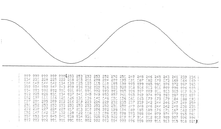
Fig. 8 Example of graphical and numerical outputs from the output memory.
Sinusoidal waveform, sampled at iOK increments/sec.
133]
.... , y ,/ ;/,/ '/
4 75 /
'•••' 1.1'..•: y. V
1 5 1 I S X ..i / . 5 1 ~ : 5
Fig- 9 Example of graphical and numerical outputs from the output memory.
Arbitrary waveform,sampled at lOK increments/sec.
2 1
8. CONCLUSION
The output data processing system for the electronic model previously contained an instrument (a standard product, 'Transient Recorder') by which the data was stored temporarily and its processing speed adjusted for the peripheral instruments of the system. This was the only part in the system, which limited the resolution of data to 6 bits. This has now been replaced by an 8-bit resolution circuit block designed for the
purpose. This block has a larger storage capacity (2.5 times) and smaller physical size (a single board), and a programmable scaling control. The block can be connected directly to the recording instruments in the system, while the previous instrument required some interfaces.
ACKNOWLEDGEMENTS
This work is part of the project commissioned by the Ministry of Industry and the Department of Energy. The author wishes to thank
Miss Kathleen Reeves-Wilkin for assisting in various parts of this work.
REFERENCES
(1) Ishiguro, S. (1979): New Input Memory,