. ' I
METEOROLOGICAL INPUT DATA PROCESSING SYSTEM
A part of the electronic model for tides and storm surges
S. Ishiguro
1979
[This document should not be cited in a published bibliography, and is supplied for the use of the recipient only].
I N S T I T U T E O F O C E A I M O B R A P H I C S C I E N C E S
\
zWormley, Godalming, Surrey, GU8 BUB.
(042-879-4141)
(Director: Dr. A. S. Laughton)
Bidston Observatory,
Birkenhead,
Merseyside, L43 7RA.
(051-652-2396)
(Assistant Director: Dr. D. E. Cartwright)
Crossway,
Taunton,
Somerset, TA1 2DW.
(0823-86211)
A part of the electronic model for tides and storm surges
Page
Abstract 3
1. Introduction 4
2. Data editing unit 5
2.1 Scheme of the data editing unit 5
2.2 Formats of tapes for standard operations 7
2.3 Circuit description 9
2.4 Physical arrangement 14
2.5 Test of the data editing unit 16
2.6 Example of a data editing operation 17
3. Computing unit 19
3.1 Typical equations to be computed 19
3.2 Maximum values of parameters 20
3.3 Example of computation scheme 21
3.4 Circuit description 26
3.5 Physical arrangement 30
3.6 Tests and adjustments 35
3.6.1 Test tapes 35
3.6.2 Synchronization 41
3.6.3 Test procedure 41
3.7 Performance 45
4. Vector plotting unit 50
4.1 Principle 50
4.2 Scheme of the vector plotting circuit 52
4.3 Circuit description 55
4.4 Physical arrangement 56
4.5 Linearity of drawing a vector '60
4.6 Formats of tapes 63
5. Operation and operating procedure 66
6. Examples of output 71
7. Conclusions 77
Acknowledgements 77
References ' 77
Appendices 1. Programme for a test pattern for 78
vector plotting
2. Example of the programme for vector 79
plotting
The meteorological input data processing system is a part of the new electronic model which is used for the dynamic analyses of tides and storm surges in most on-continental-shelf seas. This model method offers the solution of the tide and surge equations in the differential
(not difference) forms at a high speed (typically 10 milli seconds for a 10-day surge). The meteorological input data processing system is used for converting meteorological input data in an arbitrary form
(e.g. the data of atmospheric pressure represented by a set of isobar maps) into the.form which can be 'processed by the model.
The system consists of the data editing unit, computing unit, and vector plotting unit, supported by a keyboard, tape-punch, tape-reader and xy plotter.
The data editing unit is used for changing the order of data and editing it with other data, and also for producing copies of data at any stage of the data handling.
The computing unit consists of several sub-computing units which make it very versatile. It is used for computing the input data to the
stage just before its dynamic computation (which is carried out by the main computation circuit in the model). For example, the data of wind field can be computed from the data of atmospheric pressure field, by setting this unit appropriately. The stress of the water surface due to the wind field, the surge height within each finite area and time, etc. can also be computed. The speed of computation is much faster than the speed of data transfer (typically a few micro seconds for each set of computation).
The vector plotting unit has been designed to display the data in vector quantity at any stage of the computation, so that the data can be checked before the final surge heights and currents are obtained
(e.g. the computed wind field can be compared with observed wind data). The plotting speed is limited by the xy plotter (about 1.3 vectors per second at the moment).
The system is contained in a case of 7.7 x 21 x 23 cm® (weight 3.3 kgr), and operated by a 240V AC power line.
The electronic model for tides and surges (Ref. 1) requires a set of meteorological input data to simulate a storm surge. Available meteoro-logical data, however, generally varies widely in its forms (e.g. diagram, table, tape or punched card, each of which contains data in various
orders), while the form required for the model is almost fixed. This paper describes an electronic system by which meteorological data in various forms can be converted into a usable form for the model.
The system has been designed to carry out three types of operation:
, 1 To edit input data in an arbitrary format to the format required
for the main computation circuit of the model.
2 To compute the input data before the full dynamic computation is
carried out by the main computation circuit.
For example, wind field data for the sea surface is computed from atmospheric pressure field data alone. The wind field data can then be combined with the pressure field data, also by this system.
3 To display the data at any stage of processing so that the data can
be checked against other references.
For example, computed wind data can be compared with observed wind data, before it is applied to a surge computation.
MBTEOROLOGICAJ^
INPUT DATA
SURGE
OUTPUT DATA
MBTEOROLGGICAL
• I'lAIH
OUTPUT' DATA
IKPUT DATA
-IBPUT MEMORY
COI'IPUTATION
PROCESSIITG
PROCESSIITG
CIRCnjIT
SYSTEM
SYSTEM
CIRCnjIT
Fig. 1 Position of the meteorological input data
processing system in the whole model.
Fig. 1 shows the position of the meteorological input data processing system in the whole system. The system consists of
Data editing unit.
Computing unit, and
Vector plotting unit,
supported by a keyboard, tape-punch, tape-reader, and xy plotter. The tape-punch and tape-reader which are used in the present arrangement can be replaced with a magnetic tape recorder/reader, if necessary.
The data editing unit has been designed to convert input data in arbitrary format into the format required for the first stage of compu-tation which is carried out by the circuit described in chapter 3,
The basic principle of the unit
is;-^ to write the input data into a random access memory (RAM) in the
order of the data reception,
2 to read the data in the memory in the order required, and
3_ to combine the read data with other data.
This unit can also copy a tape with an arbitrary code up to 8-bit per word, while few standard tape handling apparatus accept an arbitrary code.
The memory has only 256 addresses, but this is more than enough for this application. Input data is usually related to meteorological con-ditions which are expressed by values on meteorological grids on maps with, typically, hourly intervals. Therefore, the editing operation can be repeated for each map without changing the format. The total number of the meteorological grids for which useful information is available is less than 100 for the seas around the British Isles at the moment.
2.1 Scheme of the data editing unit
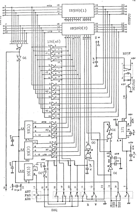
Fig. 2 shows the block diagram of the data editing unit, and Fig. 3 shows its essential parts.
Four types of input tape are
used;-Tape A which contains input data only, and is used for writing it into the memory.
Tape B which contains addresses of the memory, and from each of which a word in the memory is read.
Tape C which contains the addresses as Tape B, but also contains another set of input data which is mixed with the first set of data.
Tape 0 which contains the start code only, and used for checking the contents of the memory.
The data editing unit works in three modes
Input data given by tape A goes directly to the output, or through the memory, without changing the order of words.
2 Input data given by tape A goes to the output, in the order specified by tape B.
DATA
DATA
— D p "
TAPE COFPROL
TAPE PUNCH
TAPE SPEED
COllTROl W E CONTROL
TAPE READER
RAM
DATA FLOW
COETROL
CODE
GENERATOR p
(PERIODICAL)
MANUAL
MODE CONTROL
Fig. 2 Block diagram of the data editing unit.
INPUT
DATA
DATA
ADDRESS
i I
RAM
TAPE
READER
CODE
GENERATOR S
WRITE
MODE
ADDRESS
OR
ADDRESS
& DATA
TAPE
READ
MODE
CODE
1
1
GENERATOR P
DATA PLOW CONTROL
' OUTPUT
DATA
which generates a sequential binary code.
Read mode 1 is carried out by selecting the memory address with code generator S and by reading the memory.
Read mode 2 is carried out by feeding the address code on tape into the memory address, and reading each word corresponding to each address.
Read mode 3 is carried out by feeding the address code on tape C into the memory address through the switching circuit which is controlled by code generator P. When the switch is in the 'output side' position, the data on tape C goes directly to the output. The code from code generator P is programmed so that the address and data on tape C are separated.
The timing of the RAM is controlled by the memory control circuit which synchronizes with the tape-reader, tape-punch or manual mode selector. The write speed of the whole unit is limited by the tape-reader (500 w/s max.), and the read speed is limited by the tape-punch
(75 w/s max.) with the tape-reader in a step-by-step mode.
In order to achieve an optimum speed of operation, the whole unit is normally synchronized with the tape-reader. Only when the tape-punch is activated (even for punching a single word), the whole unit is instan-taneously synchronized with the tape-punch, then returns to the first state immediately. This action is controlled by the tape control circuit for the tape-reader.
2.2 Formats of the tapes for standard operations
The formats of tapes A, B, C and 0 are described in this paragraph. The details of the format for Tape C varies from case to case, but a typical format is shown as an example.
Tape A For the sequential writing of data into the RAM.
ADDRESS 0
1
2
3
4
254
255*
START
- -y
A
Effl)
255*
2W'
Unusable
<6
253 words
Usa'ble for data
255w
Note (1) A word of data recorded on this tape will be written at an address of the memory as specified above.
(2) Data should be represented by between 0* and 254* (not 255*)
255*
STMT
CUT+
ETTD
Note (1) Data in the memory will be read in the order of addresses specified by this tape. The same data can be read repeatedly.
(2) An address should be represented by a number between 2* and 244*.
(3) The length of the tape is not limited.
Tape C For reading data in the RAM in a particular order, and mixing
other data in the output.
255*
START A1
A2
A3 A4D1
D2
- -]
A5
A6 A7 A8 D3'
D4
--1 -1
Mm
CUT+k
8w/section
W
Note (1) A^ represents an address from which a word of data is read. (2) Dj^ represents a word of data which should go directly to the
output, after A^ to A^+g have been read.
(3) A^ should be represented by a number between 2* and 244*; and Djj by a number between 0* and 244*.
(4) The length of the tape is not limited.
Tape 0 For reading the memory written in-the order of its addresses.
255*
START
NO CODES
T
r
CUT+
END
254w
Note (1) Data in the memory will be read in the same order as the writing.
(2) If the tape is longer than 254w, the reading will be repeated in cycles.
* A number with an asterisk shows a binary number which is indicated by a decimal number in this chapter for convenience.
Tape control circuit for the tape-reader
Fig. 4 shows the circuits relevant to the tape-reader control (the circuits supplied with the standard model of the tape-reader are not shown).
The tape reader has a set of opto-electronic sensors, and generates a positive-going signal at the terminals on CN103, when there is a hole on each of the tape tracks. 8 data-tracks and one tape-feed-hole signal are available.
The tape-reader motor and clutch solenoid are activated separately by a combination of manual and electronic switches. Switch SW-FSB has three positions: F for forward run of the motor, S for stop, and B_ for backward run of the motor. At B-position, both the motor and clutch are activated by the switch itself, but at F-position, only the motor is activated by the manual switch, and the clutch is activated by the electronic switch. The motor requires about 30 ms to reach its maximum speed, and therefore this has to be switched on before the clutch is operated, when a high speed is required.
The circuits shown in the bottom part of Fig. 4 have been prepared for
:-(1) the continuous running of a tape, which is started by a manual switch, and stops by the tape-end code, '255', which is
punched on the tape, automatically;
(2) the step-by-step movement of a tape, when a read-command signal is given to the circuit;
(3) the waveform shaping of the tape-feed-hole signal, and the read-command signal, which are required for this circuit and the RAM.
The FF (flip-flop), 00/1-6, controls the clutch of the tape-reader. The negative-going signal applied to 00/2 makes a tape run, and that applied to 00/5 stops the tape. The start signal is given from either BD31/22 or BD31/29. The stop signal is given from either the shaped feed-hole signal (through 121(2)) or the '255' signal (tlirough 00/8-11 and 7492). For the latter, the '255' signal is given twice indicating the start and end of a tape, but the circuit detects the 'end' only to stop the tape. This selection is carried out by a 1/2 divider (92). Each 00/8-13, 121(1) and 121(2) is a pulse shaper by which a constant pulse width is obtained independently of that of the input signal.
In Fig. 4, a relay connected to CN103/17 and 18 is prepared for operating the tape reader with BD2. See its text for the details of its operations. When this relay is not activated, 121(2)/5 is
connected to BD30/29.
TAPE-READER
g
1
FED 16 1 0 0 6 g
1
FED g
1 BWD 19 8
OIUTCE 2 0 10
SOLEBTOID
1 0 K * l 2 9 % 13
FE
1 '
O l O
0 1 2 <-o 25
0 I 3
X
S~O 9
<-0l7
+ SHOWS +5v
> - 0 19
00 6
> - 0 16
7 <-0 24
START
<-0 11
Fig. 4 Tape control circuit for the tape-reader.
ARBITARY
g
1 2 l ( l ) / 3 , 4
12l(l)/6
00/11
92/2
00/6
r — • • - — —
1
START END
n r
END
1
1 1
Fig. 5 Timing diagram of the circuit shown in Fig. 4.
Memory and its associated circuits
Fig. 6 shows the circuit diagram of the RAM and its associated parts, and Pigs. 7 and 8 show its timing diagram.
The RAM consists of two units of MM5269, each of which is a 255 x 4 bit MOS static random access memory with three-state output. It has four control terminals, LATCH (pin 17), OE(18), CE(19) and WE(20), to each of these a signal in a different timing is required.
For WRITE, signal 'EEE' (see the previous chapter) is directly applied to the LATCH. The same signal is passed through a delay circuit
(04/8-11), and its output, which is delayed by about 13/us, is applied to CE. Another timing pulse is generated by 04/6 and 00/3 (the start of the pulse coincides with the start of pulse EEE, and its end coincides with the end of pulse CE) , and this is applied to WE. OE is kept in the low state by one of the manual switches.
For READ, signal EEE is again applied to LATCH. The output of the delay circuit is again applied to CE. The output of 04/6 is applied to OE, this time. OE is controlled by either one of the manual switches or the programmed switch, through 00/9,10.
The switching of all the data channels is carried out b y 4 sets of three-state bus-buffer gates, 74126s. The same type of gates are built in the RAM.
For the sequential-code generator, 93(1) and (2) are used so that BINARY CODE 0 to 255 are obtained.
For the meteorological-input-data programme, a simple 1/8 divider consisting of 93(3) is used at the present. This can be programmed in a more complex mode if necessary. This controls the switching of ADR mode and PAS mode alternately which results in ALT mode.
For detecting '255'.code on an input tape, a multiple input NAND gate, 30, is used. The output of this gate, inverted by 04/2 is used for resetting all the 93(1), (2) and (3).
The signal SSS is used for the clock only when the system is in WRITE MODE. This signal is generated by delaying the signal EEE. Each pulse of the SSS appears about 3 ms before the next pulse of EEE. This arrangement is important for this application, since a word on the second input tape should be sampled after the switching of ALT mode has been completed. Otherwise, the order of words in the output around the
time of the switching will be disturbed. For example, the correct output
D(n-2), D(n-l) ; MD(n), MD(n-l)
in Fig. 8 will become
D(n-l), D(n) : MD(n) , MD(n-l)
1315269(1)
m 5 2 6 9 ( 2 )
126(x6)
O
04
[image:14.599.50.524.41.759.2]SEQ
B D 3 1 - 1 2 l ( 2 ) / 5
BD3O-O4/OUT
BD31-12l(2)/l
m
DATA.
EBB
B D 3 2 - 5 2 6 9 ( l , 2 ) / l 7 LATCE
B D 3 2 - 5 2 6 9 ( l , 2 ) / l 9 ^
ED32-5269(1,2)/20 ^ -r
I —
0
H
g
H
Pi 8
02
1 2 3 4
Fig. 7 Timing diagram of the circuit shown in Fig. 6 (write mode).
SOLBIOID J[
CAM SIGUAL
SPEED COITOROL
sss
SOLENOID
m SIGNAL
CONTROL
BEE
DATA .ON TAPE
LATCH
CE
SW M3M
MEMORY INPUT
MEMORY OUTPUT
PAS INPUT
ALT OUTPUT
PUNCH SAMPLE PUNCHED TAPE
D(n-l)-J3 D(ii)—i
L O
5 P-S r- ADDRESS REQUEST
— — I n
EVERY 8 CYCLE
D(ii) D(n+1)
MD(n+l)
- D ( n - l ) - t e ^ ^
D(n-l) MD(ii) MD(n+l)
0 20 40 ms
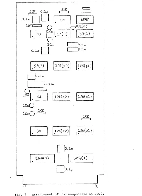
2.4 Physical arrangement
Pig. 9 shows the physical arrangement of the circuit shown in Fig. 6 .
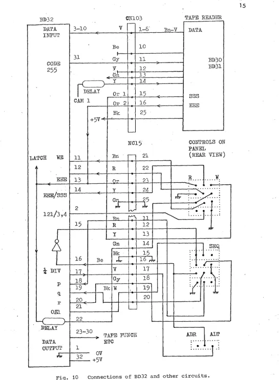
IC sockets are mounted on a standard circuit board, and pins are wired on the rear of the board. Fig. 10 shows the connections of BD32 and other circuits.
33E o . l / f 33K
CZZD
0^1/U
00
o
lOnO
lOn
121 ^ ,RS5Y
0 ' BCI84O
,93(2y 0 '
,93(1)
0 . 1 ^
2 2 ^ 22//
, 9 3 ( 3 ) 1 2 6 ( p 2 ) 1 2 6 ( p l )
0.1/,
0.22^
O lOn
I 1
04 1 2 6 ( q 2 ) 1 2 6 ( g l )
l O n Q
l O n Q
lOK
I I
30 126(r2) 1 2 6 ( r l )
0.1//
5 3 6 9 ( 2 ) 5269(1)
0.1
[image:16.603.86.544.152.785.2]CM
TIPE READER c m o 3
DATA
INPUT
Bn-v DATA
CODE 255
DELAY
CAM 1
Or 1
Or 2
CONTROLS ON
PAI^EL
(REAR 7IE¥)
latch ¥B
EBB/SSS
1 2 1 / 3 , 4
I
t DIYDELAY
2 3 - 3 0
TAPE PUNCH
[image:17.612.39.585.29.772.2]DATA OUTPUT
2.5 Test of the data editing unit
The performance of the data editing unit can be tested simply by using three test tapes. The formats of the tapes, and their correct outputs are described in this section:
Tape RAM-DATA-TEST ' For testing the write/read function of the RAM.
2 5 5 * 2 5 5 *
254* 253* 252* /
START 254* 253* 252*
(• 255*
J 2 * 1* 0* 255*
)
0* END257 words
Use this tape in WRITE MODE, and read the data in the memory in SEQ MODE (see seotion 2.2).'The correct output is:
h
-253* 252*
] £
2 * 1*257w
0 *
Tape RAM-ALT-TEST For testing ALT MODE (see section 2.2),
2 5 5 *
START 0* 1* 2* 3* 0* 1* -
-S 4 * 5* 6* 7* j 2* 3*
-"
^253* 253* 254* 254* 126* 127*
-CUT END
Write the RAM by using tape RAM-DATA-TEST, and confirm it by SEQ MODE. Then apply tape RAM-ALT-TEST. The correct output is;
1* 0* 0* 254* 253* 0* 1* -
-i
| 2 5 3 * 252* 251* 250* 2* 3* - -]
1 1 1
1 4* 3* 2* 2* 126* 127* -
-RAM-ADR-TEST For testing the ADR MODE (see section 2.2).
2 5 5 * II 0* 1* 2* 3* 4* ^ % 253* 254*1 - - 255* 258w
Write the RAM by using tape RAM-DATA-TEST, and check it by SEQ MODE. Then read the RAM in ADR MODE by using tape RAM-ADR-TEST. The
correct output is:
1* - - 254* 253* 252* ]
2.6 Example of a data editing operation
An example of a data editing operation by using the formats of Tape A and Tape C (§2.2) is demonstrated.
Suppose there is an isobar map with 133 grids. The value on each grid is read manually (or digitized) and recorded on a tape through a keyboard. The order of reading can be chosen for the operator's con-venience, e.g. from the top-left to bottom-right. The format of Tape A should be applied to this case. Then the contents of the tape will be as shown in Table 1.
2 Suppose we want to combine four pressure values read at 4 adjacent
grids which form a square a-b-c-d as shown in Fig. 11. Such a square can be formed all over the map, but take one square as an example. Since the order of such 4 values, P
a' c' Pjj in Table 1 is fixed.
the memory addresses in which these values are written are also fixed, e.g. for the first square, address 48, 49, 51, 52.
_3 If we also want to combine these 4 values with the values
represen-ting the latitude, (j), and the mean water depth of the square, h. The combined set will appear
f Ph ' Pf-' Pd' 'f'' ~
where - represent a blank.
^ The format for Tape C should be applied to this case. Memory address
48, 19, 51, 52 should be used for , A2, A3, A^ of this format (see §2.2),
and the values of cji and h (e.g. <f( - 139, h = 51) should be used for
and D
2- Then the actual tape will be
048, 049, 051, 052, 139, 051, 000, 000
The same procedure can be applied to all the squares on the map. The contents of a completed tape will be as shown in Table 2.
^ If this tape is processed by the data editing unit, after the contents
of Table 1 are written into the memory, the output of the unit will produce a series of numbers as shown in Table 3. Note, a tape in the format of Tape C can be used repeatedly for all the maps in the same form, while the contents shown in Table 1 have to be changed for each map. The processing speed is limited by the tape punch (75 ch/s), and it will take about 20s to complete Table 3.
a
Atmpspheric pressure values on an isobar map.
START A. . fc
00 a 7 ^ \ r, 04 :• 02." 045 0201 CI 0 \ 0 0 iTi-';:: 070 0 6 2
• J 4 W: i I 0 : 021 002 072. 074 022 \007 k ' 7 071 0; 0 0 \
--j .'.0 10." 12 2 1 1 - 128 110 115 |116 11 i-l 112 107 1 2 7 12
Ic.i'A i:::; i 2 0 127 120 122 145 14 2, 14 4. 154 16 175 185 1 2 2 1 2 0
025 0 2 2 02C 024 041 0b3 055 145 145 140 120 14 0 142 042 050 057
•i 60 162 i.t'S 167 172 174 ri7" 07 5 0"2 004 022 10 i 112 17? 132: 109
112 122 131 l i ' l 201 20-2 211 12:6 121 127 204 21 1. 154 147 1 5 3 154 /S;
070
121 14 M
. i ;
VG'J- VT-j VoO Ci"'-1P2 1')^ 19':' J.js
0 5 7 ) e o c 0^0 ,
END 1
Table 2 Example of contents of Tape C.
START- r 4 h he ^4 d k —
-009 [2551 048 04? 061 139 051 000 00(1 035 036 048 04? 137 080 000 000 023 024
035 0 3 6 134 098 000 003 0 1 1 012 023 024 132 1 1 4 000 000 134 0 0 2 0 1 1 012 130 149 090 000 04 9 350 062 063 14 0 075 000 000 02 6 037 043 050 138 1 1 0 000 000 024 025 0:(G 037 136 130 020 000 012 013 024 025 134 1 3 1 000 0 0 01 0 0 2 0 0 3 012 013 132 12B
000 050 0 5 1 064 142 076 000 000 037 038 050 051 1 4 0 1 1 4 000 000 025 026
037 030 137 126 000 000 0 1 3 014 025 026 135 127 000 009 0 0 3 004 013 014 133 208
000 652 053 001 0 0 2 14 4 026 000 '000 039 040 032 1 4 1 0 2 4 009 000 027 025
039 04 0 139 010 000 000 0 1 1 000 011 028 137 190 000 000 0 0 1 0 0 2 015 009 135 174 000 0 0 0 033 034 000 001 145 000 000 000 0 3 2 0 0 1 0 0 1 000 0 0 1 r< 0. 000 000 012 009 040 0 4 1 1 4 1 003 030 000 000 001 000 001 001 0 0 1 000 000 000 0 0 1 001 000 000 003 000 008 034 635 003 000 003 041 000 000 0 0 3 0 4 2 034 035 0 0 1 0 3 5 000 000 009 010 04 1 032 139 033 000 000 001 00:^ 001 000 000 033 000 000 0 3 5 000 000 001 001 0 3 :
000 000 032 025 033 032 003 032 000 000 010 0 0 1 0J.2 129 035 000 000 000 003
010 0 0 1 000 003 000 000 032 041 001 000 003 0 3 3 000 000. 0 4 3 04 0 040 0 4 1 129 032 000 000 0 3 1 032 043 044 147 019 000 000 007 0 0 3 040 041 1 4 9 0 6 3 000 000 014 011 027 008 002 00? 000 000 033 032 002 003 002 000 000 000 0 4 4 0 4 1 957 058 1 5 1 016 000 000 000 00? 001 006 011 035 000 000 028 0 2 3 0 4 1 042 1 5 1 060 000 000 015 000 008 009 000 035 000 000 002 003 034 035 001 0 3 2 000 000 0 0 1 0 0 2 002 003 1^:0 006 ^00 000 0 - 2 043 052 117 155 014 000 000 0 3 3 094 106 107 1 5 3 039 0 0 0 000 016 081 025 030 150 027 000 000 046 047 059 060 136 1 5 5 000 000 0 3 4 035 047 04 8 135 030 000 000 043 040 033 034 137 021 000 000 030 0 3 1 043 044 1 5 5 0 3 1 000 000 017 01% 030 031 152 038 000 000 047 048 060 061 137 006 000 003 0 6 2 0 6 3 1 3 2 133 163 022 008 000 034 035 042 063 166 019 000 000 04-', 1 0 3 118 ' J 9 1 5 7 0 3 2 0 0 0 000 095 096 044 109 158 029 000 000 018 019 031 032 1 5 5 033 009 000 0 1 0 0 1 1 022 019 130 160 000 000 0 4 1 042 035 040 162 020 000 0 0 0 047 04 8 057 053 1 4 6 1 6 6 000 000 034 035 0 1 1 948 144 154 000 000 021 022 034 035 1 4 1 0 3 1 000 000 048 0 4 9 058 059 148 000 030 099 100 112 113 ,145 076 000 000 086 087 099 100 1 4 2 0 7 4 000 000 100 10 j 1 1 3 114 146 064 000 000 000 000 000 000 000 000 000 000 0 0 0 0 0 0 000 000 000 000
'END •
Table 3 Example of the edited, result. The contents
of Tapes A and C are combined.
S T A R T
f A . fa fd Jl
-1
000 |255| ^ 1 1 6 11? 127 130 139 051 000 000. 1103 100 116 119 1 3 7 0 8 0 000 000 083 076
1 0 3 100 134 000 000 0 . 0 063 076 1 3 2 114 000 000 0 5 7 045 070 0 6 3 130 1 4 9
000 000 119 113 120 140 075 0 0 0 000 100 095 119 113 13 8 110 000 000 076 074
100 055 136 130 000 000 0 6 3 059 076 074 134 1 3 1 000 000 0 4 5 0 3 6 363 059 132 128
000 0 0 0 113 107 128 142 076 000 s r i M 095 090 113 107 IcLu. 1 1 4 0 0 0 000 074 072
095 090 137 126 000 000 059 056 074 072 125 127 000 000 0 3 6 0 3 1 059 056 133 20 R
000 000 127 145 143 144 090 0 0 0 000 110 104 127 '1 i 1-1 4 1 0 0 0 000 092 087
110 104 139 078 000 000 076 0 7 0 087 137 190 000 000 3 5 1 045 076 070 135 238
000 0 0 0 123 122 143 146 14 5 080 0 0 0 000 104 099 123 122 1 1 1 1 1 0 000 000 077
104 099 141 067 000 000 070 056 087 077 139 2 1 5 0 0 0 000 1 2 8 125 1 4 0 142 144 059
000 000 122 124 14 6 154 147 041 000 0 0 0 099 0 9 6 122 124 1 4 5 0 5 5 000 000 0 7 7 07]
099 0 3 6 143 0 5 5 0 0 0 000 056 040 077 071 140 225 000 000 1 2 4 1 3 1 154 1 6 1 14 9 04 5
000 000 096 100 124 147 044 0 0 0 000 071 085 0 3 6 100 145 0 3 9 000 000 040 040
0 7 1 085 142 0 0 7 0 0 0 0 ^ ' 131 140 161 175 1 5 1 039 000 000 000 0 5 0 1 2 1 140 14? 02.6
000 000 085 090 036 050 147 019 000 000 042 050 010 011 1 4 9 0 6 3 000 000 025 022
0 4 2 0 5 0 146 077 000 000 140 1 5 0 185 154 024 000 000 050 1 2 8 140 1 5 0 1 5 1 016
090 0 0 0 123 1 4 5 14 5 139 115 000 000 050 057 011 011 1 5 1 060 000 000 023 026
050 0 5 7 14 8 063 000 0 0 0 091 033 106 103 133 116 0 0 0 000 1 2 8 1 2 7 145 1 4 0 14 0 0 0
000 0 0 0 015 016 026 041 155 014 0 0 0 0 0 0 057 0 6 3 015 020 1 5 3 0 3 3 000 000 0 1 0 034
057 0 6 3 150 f • J- 7 000 000 054 051 132 128 136 155 0 0 0 000 1 0 6 1 0 3 151 116 135 094
000 0 0 0 084 092 0 4 1 040 157 001 000 000 051 0 0 2 000 000 139 0 3 1 000 000 034 04 3 0 6 3 006 152 000 l"' l"i 'S 051 052 128 127 137 070 000 000 1 3 1 137 150 1 5 4 163 022
000 000 0 - 8 058 131 137 034 003 000 000 037 048 058 157 0 2 2 000 000 070 080
092 1 0 1 158 029 000 000 055 070 080 155 0 3 3 000 000 078 0 7 0 091 0 8 3 130 164
009 0 0 0 101 "!.li. 122 131 162 020 0 00 177 1 8 3 ' -J ' 2 0 1 1 - 6 1 6 6 0 0 0 000 160
162-161 1''4 154 0 0 0 000 14 5 1 5 160 024 011 0 0 0 •> c- 189 137 142 14 b 005
090 000 1 6 . : : 189 . 145 -J >• 0 0 0 0 0 0 0 1-.5 1 4 0 1 6 2 162 1 4 2 0 1 0 000 000 i':.3 167
189 192 1 / 6 064 0 0 0 0 0 0 1 000 E N D
3. COMPUTING UNIT
The computing unit has been designed for computing a set of meteorological input data, before it is fed into the main computation circuit which carries out the dynamic computation. The computing unit consists of several
sub-units:-Six input channels, each having an 8-bit memory and DAC;
Two-dimensional gradient unit, TDG, which functions
X = (a + b - c - d) /K y = (a - b + c - d) / k
Vector-rotation unit, VUR, which functions
X = X cos 6 + Y sin 6, y = X sin 6 + Y cos 6;
Vector-sum unit, VSU, which,functions
z = v'x^ + y^
Three multiplying units, MlU, M2U, M3U;
Adding unit, ADU; and
8-bit ADC.
The combination of the units, and constants within each unit are changeable so that different equations in a similar form can be computed.
3.1 Typical equations to be computed
A typical set of equations.
Y a " @
''pi * Pi *" (Pa + Pb " Pc - P^)/2(2AX) (3)
P y = (Pa ~ Pb Pc " P(j)/2(2Ay) (4)
is used for explaining the uses of the computing unit, throughout this chapter.
In these equations.
Pa' Pb' Pc' Pd' 4" ^a (5)
are variables, and
are constants within a certain storm case. The values finally required for each grid of the model are g and g . These are obtained by dividing
equations (2) and (3) by h, where h '=^h^. These dividing operations are
carried out by two circuits contained in each grid of the model. (The
3.2 Maximum values of parameters
The maximum values of variables in the above equations should be estimated, before the flow chart is designed.
Pressure gradient
From the definition of P and P ,
X y
I f I
- 10' or (7)' ' max
has been chosen as the maximum value. This value is equivalent to the pressure gradient of 10 mb/100 km which produces approximately 45 m/s of wind speed in the North Sea, according to statistical data, An extreme wind speed in the North Sea for a recurrence period of 50 years is approxi .mately 40 m/s (hourly-mean value at the height of 10 m above the sea level) (Shellard, 1974),
Note the maximum value of \p\ is independent of the absolute
values of p^, pj^, p^ and p^.
Water depth
The present model covers the sea around the British Isles whose water depth is less than 200 m. Considering instrumental convenience
for coding the values,
|h I = 2.54 X 10^ cm (8)
' a'max
has been chosen as the maximum value.
Latitude
The lowest latitude involved in the present model is ^ = 50°, therefore
l l / s i n ' O l m a x = (9)
has been chosen. However, the code system which has been chosen for instrumental convenience can cover
below l/sin^(j) = 2.54
3.3 Example of the computation scheme
Since the construction of circuit board BD2 is versatile, it is possible to make several different flow charts even for the same set of equations.
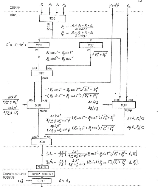
Fig. 12 shows an example of the computation scheme for Equations (1) to (4) . This illustrates the process of computing the equations by-using the same symbols as those in the original equations.
The six variables (Equation 5) are fed into the board through the input tape. Five constants (Equation 6) are set on the board for each storm case. In practice, it is not often necessary to change them.
The intermediate output is recorded on a tape to be kept perma-nently, so that this can be fed into the grids of the model, through the Input Memory, at any time. The memory can store the whole of the data until its power supply is switched off.
Fig. 13 shows the same scheme as Fig. 12, but for determining the range of values involved. Since only the maximum value of each variable is of interest, for this purpose, all the equations are shown in a
greatly simplified form. At the same time, 'voltages' and their coefficients which are required for the calibration of the circuit
board, are introduced in this chart. Their details are explained in the following paragraph.
The introduced factors are as follows
Fp = (9)
where Ep is the output of TDG, VRU and VSU. Note the operations with VRU and VSU do not involve the change of dimensions of data.
Fl ='P'/EMiAB (10)
where is the output of MlU
F. = (l/sin=(j))/E, (11)
<P 9
where E^ is the voltage representing (l/sin^^).
Fh = ha/Bh
(12)
where Ej^ is the voltage representing
E , E and E^ can be chosen arbitrarily within instrumental
limitations. However, all these values have chosen as 5V, for the sim-plicity of practical operations. For example,
BD2
MIfi MIA
M3A M3B
M2A
'"iin
'*/*%: 3 o^E S'n'
API
IWTEEICEIDIATE
OUTPUT •
OUTPUT
VSU
IJJPUT MEMORY
M3U
TDG
OUTPUT
? =
/'g
6 =
^ •=.
.-n r . ^ c . n l ^ ~ P, ]
[image:24.602.45.575.45.672.2]INPUT
BD2 ~3
O
PO vo
M I B MIA
M I A B
M/AB
MSA M 3 B
M2A M2B
f,D2 ADI
\ TAPE i
IBPUT MEMORY
OUTPUT
MIU
vsu
MZU
Fig. 13 Example of the scaling in the computation
[image:25.602.49.552.56.802.2]^MZAB output of M2U) and (the output of M3U) are added by
ADU, and this produces Ej^. If ADU has a unit gain, the factor for all
these three voltages should be the same, and this is represented by F^. Therefore,
^A ^M2AB f — ] (1/sin^ (f))
rAl
pR BM3AB = (l/sin^fihajP
Fa 2% = Sh = (^;]((l/sin
'A ^A P9 j p : +
(13)
(14)
(15)
The value of can be chosen arbitrarily in principle. In practice,
however, this should be chosen so that the maximum value of gh^ is recorded on the tape as close to its full scale (245*) as possible, but not exceeding it.
The output of ADU (in the hydrodynamic terms)
A l l
( 1 6 )
^A ®A " = y (d/sin^ (f))B
becomes a maximum when "P and h^ are maximum at the same time. Taking
their maximums as described in page 20, and taking |E^|max = 5V, F^ is determined by equation (16). The value of F^ determined in this way is not necessarily a simple number. A nearest simple number is
"A 1 . 1 X 10^ cm'V 1 (17)
When F^ is fixed to this value, the values of related terms become as follows
gh = 548.716 X 10^ cm'
a' max
for
also
iBalmax = 4-9883
l/sin^(j)| = 1.70
h = 2.54 X 10
' a'max
I max = 10 -3
S = 21.603
V
cm
— 2 —2
gr cm s
cm
ej = 4.3206 x 10
for Kg = 5 X 10"^
-3 V
cm V - 1
( 1 8 )
Note, the conditions which make gh^ or maximum are not necessarily equal to the conditions which make g or e^ maximum, since h^ and h are involved. For example,
gh = 419.640 X 10' cm=
= 3.8149 V
l/sin^<j) = 1 . 7 0
for ^a =
^ =
103 10"^
cm
- 2 - 2
gr cm s
also
c = 4 1 8 . 6 4 cm
®1 = 8 1 . 9 2 8 X 10 ^ V
for Kg = 5 X lo" -3 cm V - 1
C and e^ in the latter is far greater than
(19) A summary of the main factors is given as follows
F = 2 . 0 0 0 X 10~^ gr cm~^s~\~^ F, = 3.400 X 10"* V~*
4"
F, = 5.000 X 10"* cm V~* h
5 -1
F, = 1.100 X 10 cm'V
A
K = 5 X 10^ • cm V~*
e
The practical procedure of setting these factors on a circuit board BD2 is described in section 3.6.
Both the two input voltages, E j ^ 2 a ^ and MU2
become maximum (both 5V) when p = 10 (CGS units) and 1/sin^ cf) = 1.70.
Applying the above mentioned value of the output voltage of MU2 is
obtained from equation (14),
EM2AB = (l/sin:*)B B ' P * (20)
= 3.7668 V
Similarly, both the two input voltages, E^^^ and of MU3 ^
become maximum (both 5V) when ^ = 10 (CGS units) and h^ = 2.45 x 10 cm. The output voltage of MU3 is obtained from equation (15),
®M3AB = J _ P
FT, ipgr a
( 2 1 )
3.4 Circuit description
Fig. 14 (a, b, c) shows the circuit of the computing unit. Fig. 15 shows its timing diagram.
Input data represented by 8-bit binary words enters into the computing unit, together with a synchronization signal, PH (the top-left of Fig. 14). The data is fed into 6 sets of data holders, a^, a.2 ... h^, h2 (12 IC
packages of 75). Each set of the data holders is activated sequentially by a timing circuit 155, so that each holder can hold one particular word at a time. After a set of 6 words have entered, the 6 words are held
simultaneously until one cycle of operation (typically a few milli seconds) has been completed.
Each of the 6 words is converted into an analogue voltage, by 6 sets of DACs (425s) with their output circuits (747s). The channels of these
voltages are indicated by a, b, c, d, h in the right side of Fig. 14a
and the left side of Fig. 14b.
The voltages, a, b, c, d, are permanently fed into circuit TDG (the top left of Fig. 14b) by which the differences of the 4 voltages are computed. The output of this circuit which represents the values of ij) and h are fed into the rest of the computing sub units, VSU, VRU, MlU, M2U, M3U, and AD, in various combinations depending on the computation required.
The output of the computing sub units is digitized by a DAC (425), after it is passed through a scaling circuit. Other than the final out-put of the comout-putation, the outout-puts from most stages of comout-putation can be selected by selector TO and TL (Fig. i4c), and are digitized by the same DAC, for intermediate checking. The selector can also select a standard voltage for a calibration.
425(x6) lok 20k
7 4 7 ( a t )
7 4 7 ( c a )
747 ( A
^f 6 channelB identical
5 /
2,8 14
Fig. 14(a) Circuit diagram of computing circuit BD2.
[image:29.599.48.587.43.765.2]To
7SU(2)
MlAB lOKxB
'vW-+ / 10
747(13:1 )
All Rs 10 K
-AW v w
+ ^ 10
747(1 y | )
747(37)
L O O K 4 . 7 IF J R Y
2 0 K 6
M I Z O 5 0 K 1 5 V + 5 V
MIZA 20K
M I Z B 20K
- ) 5 V 10K
I 5L'-H 1 5 V 747 (V)
t o k 6
M2Z0
M2ZA
SIN 'JOOK
COS '
]X}200(z2) , PDl o
PD2 0
M3ZA
3. 6. 6. 10. 10
M2ZB
To
780(1)
M2AB
SI 32 0 - 1 5 V + 1 5 V
Fig. 14(b) Circuit diagram of computing circuit BD2,
[image:30.597.26.575.26.790.2]1 5 V
7
BIAS ON R
OFF o""
ADP R1
747 (FF)
A D l o >
10 K •FROM
M3AB
+ 1 5 /
STABILIZED
Be CL
Z
Gy
TL430L
+50ppni/°C
B8 R8
100K 100K
— « v w —
G8 ElO
10 K 24 K
747 (FF) PXI i)Y m D V Ml M2 M3 AD Bn 10
1 1 1 2
1 3
1 4
| 5
1 6
1 7 Bk
NO — d ^ c b & h PX -5-NC Bn
p y ^ _ L Gy
Gy
Bk 10
1 0
-d—I
4^-o TO
-o T1
FROM
747(FB')/io
1 5 . 1 6
I
FUNGS •COMMD O(MSB) 7(LSB) CIMONFig. 14(c) Circuit diagram of computing circuit BD2,
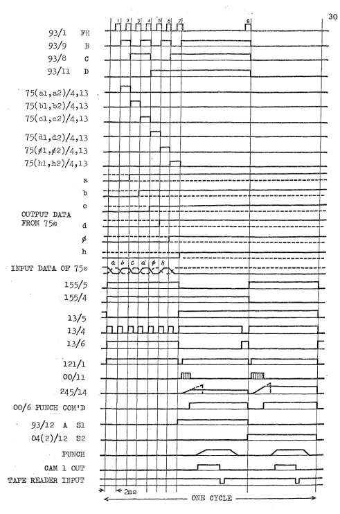
[image:31.601.58.571.27.778.2]93/1
FH
93/9
B
93/8
C
9 3 / 1 1
D
7 5 ( a l , a 2 ) / 4 , 1 3
7 5 ( t l , l ) 2 ) / 4 , 1 3
7 5 ( o l , c 2 ) / 4 , 1 3
7 5 ( < i l , a 2 ) / 4 , 1 3
75(A,j^2)/4,13
7 5 ( h l , h 2 ) / 4 , 1 3
a
"b
c
OUTPUT DATA
FROM 75s
df
imPUT DATA OF 75s
155/5
155/4
13/5
13/4
13/6
121/1
00/11
245/14
00/6
PUNCH COM'D
9 3 / 1 2
A 81
0 4 ( 2 ) / l 2
S2
PUNCH
CAM 1 OUT
TAPE READER INPUT
J l f
a n
j j O .
[ih
I
[ L A
^ 2m8
£]_
j m L
"LT
X
_Z_
J
L
ONE CYCLE
[image:32.601.36.527.31.773.2]3,5 Physical arrangement
Fig. 15 shows the board on which all the components of the computing unit are mounted. Micro connectors have been used for jump wires by which the combinations of computing sub units can be changed. Semi fixed potentiometers have been colour-coded according to their functions.
Fig. 17 and Fig. 18 show the whole unit (BD2) contained in a case. This case also contains the vector plotting unit (BD33), and power supplies (+5V lA and ±15V 0.2A). A heat sink for the power supplies has been mounted outside the case.
Control switches for both the computing unit and vector plotting unit are mounted on the front panel of the case. The outer dimensions of the case are 7.5 x 21 x 23 cm^, and the weight of the whole system is 3.3 kgr.
Table 4 shows the pin connections related to BD2.
Table 4 Connections of BD2
Main cabinet Cable
internal wire CN6 wire Met-Input-Data
colour colour rruu.
Bn 1 Bn BD2/8 (MSB)
R ^ En 2 R 7
Or n pj 3 Or 6
Y 4 Y 5
Gn < 5 Gn 4
Be < 6 Be 3
V Q 7 V 2
Gy 8 Gy 1 (LSB)
W
-9 W BD2/15 FH
— 10 Bk
-Gy 11 Gn-D BD2/47 (LSB)
V 12 P 46
Be g 13 Be/R 45
Gn
§
14 Gn/R 53y
< 15 Y/R 52
Or 16 W/R 51
R o 17 Bk/R 50
Bn 18 Bn/R 49 (RMS)
Gy/Gn 19 Y/Be SG4 Be
Bn/Be 20 W/Be Gy
Gy/Bn 21 Bk/Be V
22 Or/Be
23 y/Gn
Common
24 W/Gn Common
1
]•[
1 R 2 J2J—
R 13
^ J- 5 _
-R-12_ j-a_ 8 LKJ
TL/
R E P
L—
-=4-ADZ
l O K
JLDP
l o K
CM
' § m o\ m
H
Z a F a l O K 2 0 K
. 4 2 5 ( a )
r30]j
a
D2C = ]
D 1
o
G 8l O K
C O S B l I T 0 0 8 TOOK l O K l O O K \ 0 K
433B
Z D 21 0 K
3 d Z l C = ]
747 ( a t )
747(9)'
Z D l K
C = 3
. 4 2 5 ( t )
747(V)'
O
l O K Z h F b2 0 K F V
2 0 K
I
I
1 4 9 4 ( 3 )
741
.747 ( 3 y )
CZZJ [ = • [ I — 1
D
tr-«
DQ
•
DD
o
rn
M 3 Z 0 5 0 K
M3ZA
2 OK
/^llD206"^\
I 1 C
I 1 c
l o K
Zj
lOK
4 2 5 ( c )
O
Z c P c 1 0 K 2 O K
rn
ir\
1 1
W 3 Z B M I Z B M I Z O M I Z A
2 0 K 2 0 K 5 0 K 2 0 K 7 4 7 ( o d )
I 1
h,
t—•
o o
FG
5 K
M 3 F 1 OK
1 4 9 4 ( 1 )
c
r — I
P C 1 0 K
M I F
1 oo<
3 I 1 • I 1
747(W12)
M2F
5 0 K
o
o
. 4 2 5 ( d )
Z d . F d 1 O K ' 2 0 K
LPi
CM CM
Z V M 2 Z B M 2 Z 0 M 2 Z A l O K 2 0 K 5 0 K 2 0 K
4 2 5 ( / )
] o
1 4 9 4 ( 2 )
Z ^ F | ! ( 1 0 K 2 0 K
%
o
CM
rQ m
y
L O i
ir\
r—
CO o
ir\
o
(M •ti ir\ Sr~ CM ir\ CM f-Jd ir\ c— r-t "@L m LOi CM Z h 1 oK, Fh
2 0 K
o
4
c— c— o rn( S ) ( ^ ( 9 ) 0 - s
e
BD2
SIDE COVER 'WI'TH VEM-ILATION HOLES
e e e
m
•CABLES
OJ OJ
3.6 Tests and adjustments
The full tests and adjustments of board BD2 are necessary only when this is assembled for the first time, or when some of its components are replaced. For a normal operation, the test by using test tape BD2TT-254/ 154-100/0 which takes only a few minutes will be enough to confirm the performance of the whole system.
When the values of some constants in the equations involved are altered, a few constant-setting potentiometers have to be adjusted, but these will not affect other settings.
Fig. 19 shows the locations of components relating to the tests and adjustments of BD2. After the adjustments, each component is sealed by a piece of PVC tape which is colour-coded as
follows:-Output-scale setting (Green)
Zero setting (Blue)
Full-scale setting (Yellow)
Constant setting (Red)
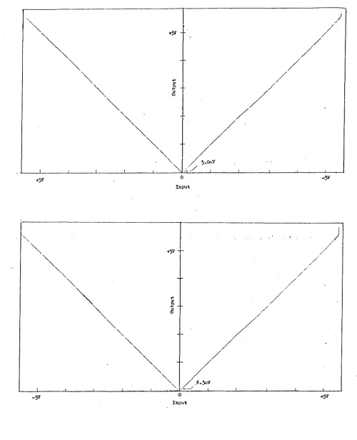
The full tests require the test tapes (see the following section) and tlie following instruments
Standard voltage source, 5.000V 4-digit digital voltmeter
Sine-wave voltage generator, 1 kHz, 5V approx., low output impedance
Cautions , , , , . , .
Due to two CMOS devices contained in BD2, the following points should be noted
^ When the power supplies of BD2 are off, no external voltage must be applied to terminals PXY, DO, SX, SY.
b When BD2 is operational, terminals PXY and DO must not be earthed.
3.6.1 Test tape formats
In order to test the computing circuit on board BD2, a set of test tapes have been prepared, as shown in Table 5. All the tapes are 8-track punched tapes, using the natural binary code. However, each binary
figure is indicated by an equivalent decimal figure, throughout this chapter. For example, binary 1100 1000 by decimal 254.
Table 5 List of test tapes for BD2
Reference No. Application
BD2TT-0 To set all the input channels to zero.
-200a To set channel a to the full scale.
-200b b
-200c c
-200d d
- 1 7 0 * <(>
-254h h
-100(j)VR To test the variation of (j).
-lOOhVR h.
ADZ! X :f.
ADP
i Za
m
.::L. ::ir
mmmm
1 Zb Fb
.^;;cl c l3 a:; PY PX %:%!: a
ST s x 1 1 : :
•
mm
Id::
:%:c
i
•
I 01
M3zo(m:^ j ' g g
Zy
i i i
Zc Fc
M3ZA ,, f, &
t M1ZA( t M3ZB MIZB MIZO M1ZA( t t
n
lix:::
M 3 B W
giSPXY Ph :;
m
•
:lt
PG W M3P
. '• MiP
m m COM
M2P Zd j i
!:A])2 MZAH ZV M2ZB M2Z0 MO ZJ^
11 fi XI
g S H . r w
-i -i -i l -i l
z/ p /
11
1 1
11
Zh
Ph
>rzvm<>y.m
•
III
i 0 # : : M 3 A B ADl
Hiitik-i'i" I'r* •*»bf
Test tape BD2TT-0
This tape has no word, but has tape-feed holes only. The tape should be a few metres in length, or an endless form about 10 cm in diameter.
Test tapes BD2TT-200a to BD2TT-200d
Table 6 Format of the tapes
Ref. No. START 1 2 3 4 5 6 7 8
Ref. No.
<P
8
CODE a b c d <P h
BD2TT-200a 255 200 000 000 000 000 000 000 000
b 255 000 200 000 000 000 000 000 000
c 255 000 000 200 000 000 000 000 000
d 255 000 000 000 200 000 000 000 000
Each tape starts with code '255', followed by 40 cycles of codes indicated by 1 to 8 in the table. Code 200 represents
-3 -2 -2
2 = 2 X 10 gr cm s
which is taken as the maximum value of T in Fig. 13.
Test tapes BD2TT-170^ and BD2TT-254h
Table 7 Format of the tapes
Ref. No. START 1 2 3 • 4 5 6 7 a
Ref. No.
CODE d
a
CODE a b c d h
BD2TT-170({) 255 000 000 000 000 170 000 000 000
-254h 255 000 000 000 000 000 254 000 000
Each tape starts with code '255', followed by 40 cycles of codes indicated by 1 to 8 in the above table. Code 170 represents
1/sin^ (j) = 1.70
and code 254 represents
h^ = 2.54 X 10^ cm
Test tape BD2TT-254/154-100/0
Table
8
Format of the tape
START
CODE
i
1
2
3
4
5
6
7
8
START
CODE
i
a
b
c
d
h .
- —255
254
254
154
154
170
254
000
o o a
154
154
254.
254
170
254
000
000
254
154
254
154
170 .
254
000
000
154
254
154
254
170
254
000
000
000
000
000
000
000
000
000
000
255
100
100
000
170
254
000
000
000
000
000
100
100
170
254
000
000
100
000
100
000
170
254
000
000
000
100
000
100
170
254
000
000
Table 9
Theoretical values of the output from the tape
shoim in Table 8.
1
2
3
4
5
6
7
8
X
y
X
y
X
y
X
y
PXY
254
127
0
127
127
254
127
0
D
79
245
175
9
9
79
245
175
V
254
254
254
254
254
254
254
254
Ml
175
9
79
245
245
175
9
79
M2
91
216
163
38
38
91
216
163
M3
96
127
158
127
127
96
127
158
AD
194
38
60
216
216
194
38
60
Test tape BD2TT-100*VR
This tape represents the value of l/sin*# varying from 0 to 1.70 with 0.05 steps, while all other values are fixed as follows:
In 'even section'
= 2.54 X 10^ cm ha = 2.54
Pa = 10-3 gr cm -1 -1 s. Pa = 0
Pb = 10-3 gr cm — 1 — 1 s Pb = 0
Pc = 0 Pc = 10-3
Pd = 0 Pd = 10-3
In 'odd section'
10'^ cm
gr cm" •1 c-l
- 1 - 1 gr cm ^ s ^
Code 100 in the tape reference number indicates that the maximum value of p^ etc. is taken as 10"^ gr cm * s *
Table 10 Format of the tape
Pa Pb Po Pd / h
Pa Pb
Pd
h-START
0 0 0 0 0 0 0 0 0 0 0 0 0 0 0 0 0 0 0 0 0 0 0 1 0 0 0 0 .4 0 0 5 4 0 0 0 0 0 0 0 0 0 0 0 1 0 0 0 0 * 0 0 2 5 0 0 0 0 0 0 0 0 .1 0 0 0 0 0 0 0 0 0 5 5 4 0 0 0 0 0 0 0 0 0 0 0 0 1 0 0 0 cr 2 5 4 0 0 0 0 0 0 .4 0 0 •1 0 0 0 0 0 0 0 0 A •i 0 5 4 rj-i 0 0 0 0 0 1 0 0 ••f 0 0 2 5 ^ ^ 0 0 0 .i 0 0 0 0 0 0 0 0 0 A .1 5 c- d 0 0 0 0 0 9 0 0 0 VI 0 1 0 0 0 0 •i x C| 0 0 0 0 0 0 0 0 0 0 0 2 0 c! C" 4 0 0 0 0 0 0 9 0 0 0 0 0 1 0 0 0 0 A 0 2 5 4 0 0 0 0 0 .< 0 0 0 0 0 0 0 0 0 0 j • j 0 0 0 0 0 9 VI 0 0 0 e 0 0 0 0 0 0 0 0 0 0 0 0 0 1 0 0 2 0 0 0 0 0 8 •?. 0 0 0 0 0 0 6 0 0 0 0 0 0 0 2 0 0 0 V1 0 0 f i i 5 •i 0 0 0 0 0 0 y 0 0 0 1 0 0 0 'Tj -I C; 6 0 0 0 0 1 0 0 0 0 0 0 0 0 0 0 0 0 0 0 0 0 0 0 0 2 9 0 0 0 0 0 0 .4 0 2 5 i". 0 0 0 0 0 0 0 0 0 0 0 0 0 M 0 0 A 4 0 0 0 0 0 0 0 0 0 0 1 0 0 0 •?, ± 4 5 4 0 0 0 0 0 0 0 K 0 0 0 0 0 0 0 0 7 0 0 M 0 0 0 0 0 0 0 0 0 Z 0 2 2 0 1 7 0 0 0 0 0 0 0 0 0 0 0 0 0 0 5 5 4 6 0 0 0 0 0 0 w 2 0 0 0 .f 1 8 6 0 0 0 0 0 2 0 0 0 0 0 0 •i 6 0 4 5 0 0 0 0 0 0 0 0 ?. 0 3 2 0 2 A 0 0 4 0 0 0 0 o 2 0 0 0 0 0 0 0 0 2 0 0 0 0 0 0
Test tape BD2TT-lQ0hVR
This tape represents the value of h^ varying from 0 to 2.54 x 10 cm with 10^ cm steps, while all other values are fixed as follows:
In 'even section'
l/sin'* = 1.70
p^ = 10"^ gr cm"* s~*
Pj^ = 10"^ gr cm * s~*
Pc = 0
p , = 0
In 'odd section'
1/sin^ (f) = 1.70
= 0
= 0
= 1 0 Pb
Pc
Pa = 10
-3 -1 -1
gr cm s
-3 -1 -1
gr cm s
Code 100 in the tape reference number indicates that the maximum value of p etc. is taken as 10"^ gr cm"^ s"^.
Table 11 Format of the tape
Pa / P a Pb P( Pd h.
-START
i d ? 0 0 0 0 0 0 0 0 0 0 0 0 0 0 0 0 0 0 .4 0 0
.-t
0 0 0 0 0 0 0 1 7 0 0 0 0 0 0 0 0 0 0 0 0 f- 0 0 0 0 0 1 7 0 0 0 0 0 0 0 0 9 .4J.
1 0 0 0 0 0 0 0•i
'r
-i.
1 0 1 0 0 0 0 0 0 0 0 0 0 0 0•-0 •-0 -i 7 0 1 0 9 0 0 0 0 0
A
0•I
0 0 0 0 0 0 1 7 0 0 L 0 0 0 0 00
0 0 0 0 05
06
1 7 0 0 0 0 0 0 0 0 00
0 G 000
0 0 0 1 7 0 0 0 0 0 0 0 0 0 0 0 9 0 0 ± 0 0•j
0 0 X 7 0 0 0 0 0 0 0 0 i 0 0 - < 0 0 0 0 0 0 '3 0 1 7 0 0 4 0 0 0 0 0 0 0 0 0 0 0 0 0 .1 J. 0 0 1 0 0 .1 7 0 0 4 0 0 0 0 0 0 0 G 1 0 0 0 0 0 0 00
1 7 0 05
0 0 0 0 000
0 0 0
0
0 A 0 0 0J.
0c
00
0 0 0 0 e 0 G 0 0 0 0 0 0 0 0 G 0 0 0 0 0 0 0 0M
0 0 •i 0 0 Gi
7 0 0 6 0 0 000
i 0 0 0 0 0 0 0 0 1 7 0 0 7 0 0 0 0 0 0 0M 9
a 0 0 10
.<
0 ± 7 0 0 0 0 0 0 0 0 0 y 6 f. 0
00 00
0 1 7 0 0 0 0 0 0 0 0 0 0 0 0 0 0 0 < Cj G i 7 0 0 0 0 0 0 0 0.i
J.
0 0 G 0 0 0 0 0 0 1 7 0 0 9 0000
0 0 0 0 0 000 M
i
0
.I0
i
7 0 0q
9 0 0 0 0 •?. 0 1 0 0 10
00 0 0
0
0 0 1 7 0 0 0 0 0 0 0 09
0 0 0 1 0 0.i 0
0 AJ-
7 0 .4 0 0 0 0 0 0 0.i
J. 0 0 10
0000
•0 0 0 1 7 0 j 1 000
00
0 0 0 0 0 00
0 •10 0
1 7 0 000
0 0 0 0 i 0 0 •1. 0 9 0 0 0 0 0 1 7 0 1 2 000
0 0 0 0 0 0 0 0 0.-f
0 0J.
0 0X
7 0 •1 2 0 0 0 0 0 0 0 ,«{0
y•i
0 000
0 0 0 1 7 0 1 0 0 0 0 0 0 00
0 0 0 0 i 0J. 0 0
.4
•i 7 01
0 0 0 0" 0 0 0 J. A0 0 1 0 0
0 0 0 0 0 0 1 7 0 1 4 00 0 0 0
00
0
0
y 0 0 0 AJ.
00 •j 0 0
J. 7 0 1 0 0 0 0 0d 0 •1
0 0 1 0 0 0 0 0 0 0 0 1 7 0J.
5 0 0 0 000
00
0 00
0 00 X
J. 0
0j
7 0 1 500
0 0 0 0i 0
0-1 00
0 0 0 0 1 7 0 1 G 0 0 0 0 0 0 000
0 0 0 1 0 0 10 0
1 7 0 -1 G 0 0 0 000
j 0 0 0000
0 0 0 1 7 0 1 7 00 0
0 0 0 0 0 9 0 0 0•1
0 0 .i0
0 AJ.
7 0i
0 0 0 900
0 i00 •1
0 0 0 0 0 0 0 1 7 0 j 0 0 00
000
0 0 0 "00
0X
J.
0 0 100
1 7 0 i 0 0 00 0
0 00
1 0 0 000
0 0 0 1 7 0 1 0 0 0 0 000
0 0 00 0
9 J. .4 0 0 j 0 0 1i
0 00
9 0100
100 0
0 0 0 0 0 1 7 0cL
0 0 0 0 0000
00 X
0 "10 1 0 13
0.i
7 0 2 9 0 9 90 9
9•1
0 0 0 0 0 0 0 0 0 1 7 0 2 A 0 0 0 00
00
0 7i Ji 0 j 0 ± 0 'J. 0i
7 0 2i
0 0 0 0 0 "i1 0
0 < 0 030 00
0 1 7 0 2 0 0 0 00 0 0
0 0 ? 0 0 0 1 0 0 •1 •i 00
0 0 0 0 0 0 G 0 0 0 0 1 7 0 1 G 0 0 00
0 0 0 0 Ci '1 0 0 •1 7 0 .4 6 0 9 9 0 0 0 0 G 0G
0 3 0 0 1 7 0 G 0 0 0 0 0 0 0 00
0 0 0 0G
1 2 2 1 7 0 9 0 3 9 9 0j j
0 0.4
0 0 0 0 0 00
1 7 0 Cj 0 0 0 000
0 ;i D 0 0 .40
0 i9
•i 7 0 53
0 9 9 9 ? 9 < 0 0.4
j 0 0 0 00
0 1 7 0 5 400
00
0 0 0 0 0 .i 0 0 •<••1 3
7 0 90
3 0-•i M Tl 30
09 Ci M
0L-i M P
f-! M
0 0 03.6.2 Synchronization
It is necessary to test the synchronization between BD2 and other circuits before further tests or calibrations are carried out.
The procedure of testing the synchronization is as follows:
1 Set the main control selector (on the main control panel) to TED.
2 Set test tape BD2TT-0 on the tape-reader.
3 Run the motor of the tape-punch.
4 Turn switch FB (on the tape-reader) to B, and leave two switches in
GE and R positions respectively,
5 Press switch TAPE FORWARD (green arrow on the tape-punch) momentarily.
If the whole system is working properly, the input and output tapes will run in synchronization. When correctly synchronized, 2 increments on the output tape correspond to 8 increments on the output tape.
3.6.3 Test procedure
For the later paragraphs (1) to (8), test procedures are expressed in a simplified form of tables. For example,
Input (V) Adjust Output (V)
SY = +5.00 Fx TX = +3.50
should be read as:- "Feed +5.00V to input terminal SY, and adjust preset resistor Fx to obtain +3.50V at output terminal TX." Also, for example, "SW2 to CL" should be read as "Set switch 2 to CL side." See page 67 for symbols.
(1) Calibration of the standard voltage on BD2
SW2 (MIP panel) to CL
SW ( " ) to F
TO ( " ) to DVM (4 digit)
Then adjust REF (on BD2) to obtain +5.00V at TO.
(2) Calibration of the tape output scale
Main function control
(on the main control cabinet) to TED
SW-VN (MIP panel) to N
SW-FB (Tape-reader) to F
Momentum SW (Keyboard) Press