Precision Full-Wave Rectifier Using Two DDCCs
Montree Kumngern
Department of Telecommunications Engineering, Faculty of Engineering, King Mongkut’s Institute of Technology Ladkrabang, Bangkok, Thailand
E-mail: [email protected]
ReceivedFebruary 22, 2011; revised April 12, 2011; accepted April 19, 2011
Abstract
A new precision full-wave rectifier employing only two differential difference current conveyors, which is very suitable for CMOS technology implementation, is presented. The proposed rectifier is the voltage-mode circuit, which offers high-input and low-output impedance hence it can be directly connected to load without using any buffer circuits. PSPICE is used to verify the circuit performance. Simulated rectifier results based- on a 0.5 µm CMOS technology with ±2.5 V supply voltage demonstrates high precision rectification and excellent temperature stability. In addition, the application of proposed rectifier to pseudo RMS-to-DC con-version is also introduced.
Keywords:Full-Wave Rectifier, Voltage-Mode Circuit, DDCC, RMS-to-DC Conversion
1. Introduction
Full-wave rectifier is used in RF demodulator, piecewise linear function generator, AC voltmeter, watt meter and various nonlinear analog signal processing circuits. Typ-ically, a conventional rectifier could be realized by using diodes for it rectification. However, this circuit would not be capable of rectifying incoming signals whose am-plitudes are less than the threshold voltage (approxi-mately 0.7 V for silicon diode and 0.3 for germanium diode). As a result, diode-only rectifiers are normally used in only those applications in which the precision in the range of threshold voltage is insignificant, such as RF demodulators and DC voltage supply rectifiers. For high precision applications, the diode-only rectifier cannot be used. This can be overcome by using integrated circuit rectifiers instead. The precision rectifiers based on op-erational amplifier (op-amp), diodes and resistors are presented [1-4]. However, the classical problem with conventional precision rectifiers based on op-amps and diodes is that during the non-conduction/conduction transition of the diodes, the op-amps must recover with a finite small-signal, dv/dt, (slew-rate) resulting in signifi-cant distortion during the zero crossing of the input sig-nal. The use of the high slew-rate op-amps does not solve this problem because it is a small signal transient prob-lem. The gain-bandwidth is a parameter of op-amp that limits the high frequency performance of this scheme. Moreover, since these structures use the op-amp and the
resistors; therefore these circuits are not suitable for IC fabrication. Second-generation current conveyors (CCIIs) is possessed a very high slew rate and bandwidth if com-pared to the traditional op-amp. This makes the CCII of primary importance in the design of modern analog inte-grated circuits.
Several circuits based on CCII for realizing full-wave rectification have been reported in the literature [5-10]. The rectifier circuit in [5-7] employ diodes and resistors in addition to CCIIs. The circuit proposed in [8] employs bipolar current mirrors in addition to a CCII and a num-ber of resistors. The rectifier circuit in [9] employs four CCCIIs and resistors. The circuit proposed in [10] em-ploys two CCII and two MOS transistors. However, the use of resistor makes these circuits not ideal for integra-tion. Recently, Chiu et al. [11] proposed a new current
conveyor circuit called the differential difference current conveyor (DDCC). The DDCC has the advantages of both the CCII and the differential difference amplifier (DDA) (such as high input impedance and arithmetic operation capability).
to-DC conversion is also introduced.
2. Circuit Realization
The electrical symbol of DDCC is shown in Figure 1.
The DDCC has three voltage input terminals: Y1, Y2 and Y3, which have high input impedance. The terminal X isa
low impedance input terminal. There is a high impedance current output terminal Z. The CMOS realization for
DDCC is shown in Figure 2 [11]. The input-output
cha-racteristics of the ideal DDCC is described as
1 1 2 2 3 3
1 1 1 0
0 0 0 0
0 0 0 0
0 0 0 0
0 0 0 1
X Y Y Y Y Y Y X Z V V I V I V I I I (1)
The proposed full-wave rectifier circuit is shown in
Figure 3. The circuit employs only two DDCCs.
Com-pared to previous rectifiers, the proposed rectifier is higher suitable for IC implementation. The DDCC1 and
DDCC2 are operated as non-inverting and inverting
uni-ty-gain voltage buffers. The input voltage Vin is
con-nected to Y1 and Y2 terminals of DDCC1 and DDCC2,
respectively, while two outputs (X terminals) are
con-nected. In this case, only positive peak will be appeared at the output voltage Vout.
The operation of the proposed full-wave rectifier is as follows: when Vin > 0, the DDCC1 is on, the voltage Vin
is followed by the DDCC1 to the voltage Vout at X
termi-nal. In addition, when Vin < 0, the voltage –Vin is
fol-lowed by the DDCC2 to the voltage Vout at X terminal
(–VY2 = VX). From the operation of the proposed full-
wave rectifier explained, the relations between the input voltage, Vin, and the output voltage, Vout, can be
ex-pressed as
1 2
0 ; : DDCC on
0 ; : DDCC on
in out in
in out in
V V V
V V V
(2)
The output voltage of the circuit in Figure 3 can be
expressed as
DDCC Y 1
X
I Z Z Y 2
Y 3
I X I Y3
I Y2 I Y1
V Y3 V Y2 V Y1
V X
V Z
Figure 1. Electrical symbol for DDCC.
VDD
M1
VSS
X
Y2 M2 M3 M4
M5 M6
M9 M10
M7
VB
Y3 Z
M8
Y1
M11 M12
Figure 2. CMOS implementation for DDCC.
DDCC1 Y 1
X Z Y 2
Y 3 Vin
DDCC2
Y 3 X
Z Y 2
Y 1
Vout
Vc
Figure 3. Proposed full-wave rectifier using DDCCs.
out in
V V (3) Therefore, the proposed circuit provides the full-wave rectification. It can be noted that the proposed circuit has high-input and low-output terminal, hence it is easy to drive loads without using a buffering device. The DC offset output voltage can be controlled by adjusting the voltage VC.
3. Simulation Results
The proposed full-wave rectifier is simulated using PSPICE program to verify the given theoretical analysis. The DDCCs are simulated using CMOS structure of
Figure 2 that can be implemented using CMOS
struc-tures DDCC given in [12]. The aspect ratios of the MOS transistors of the CMOS DDCC are given in Table 1.
The device model parameters used for the PSPICE simulation are taken from MIETEC 0.5 m CMOS process [12]. The supply voltages are selected as VDD =
–VSS = 2.5 V and the bias voltage is set as VB = –1.7 V.
voltage ranging from –1 V to 1 V of the input voltage. The magnified zero crossing of Figure 4 is shown in Figure 5. In this figure, the blunting region (b) is found
as –2.5 mV < Vin < 2.5 mV. Applying the 200 m Vpeak
sine wave at the input of the proposed rectifier, the input and output signals at frequencies of 500 kHz and 1 MHz are shown in Figures 6 and 7, respectively. This results
is confirms the operation that the proposed rectifier can provide the full-wave rectification at the input signal amplitude lower than the threshold voltage of diode (< 0.3 V). It is evident from Figures 6 and 7 that
undis-torted full-wave rectified signals are produced at all two frequencies. However, as the input frequency increases to 1MHz and beyond, the output signals have errors at the crossover region, called “corner distortion”. This corner distortion results from the non-conduction/con- ction transition problem of DDCCs. At the frequency of 1 MHz, we simulate the temperature performance of the proposed full-wave rectifier as shown in Figure 3 by
changing temperatures from 50˚C to 100˚C. Figure 8
shows the output waveform of the proposed rectifier at temperatures of 50˚C, 75˚C and 100˚C. From simulation results in Figure 8, they show that the proposed circuit
provides excellence temperature stability. This result is confirmed by Equation (3). The simulated peak outputs
Vout for the circuit were 199.46 mV and 196.67 mV at
50˚C and 100˚C, respectively.
Table 1. Transistor aspect ratios of the used DDCC.
Transistor W (m) L (m)
M1-M4 1.6 1
M5-M6 8 1
M7-M9 20 1
M10-M11 29 1
M12-M14 90 1
Figure 4. Simulated results for DC transfer characteristic.
Figure 5. Simulated results for DC transfer characteristic at zero crossing regions.
Figure 6. Operation of the proposed full-wave rectifier at 500 kHz frequency for Vin = 200 mV peak.
Figure 8. Operation of the proposed full-wave rectifier at different temperatures.
4. Application Examples
To show the advantage of proposed rectifier, author de-scribes a pseudo root-mean-square (RMS)-to-DC con-version as an example. The well-known average value of a signal magnitude is defined by
0 1 d T avgV v t
T
t (4)where v(t) is the AC signal, T is its period, and Vavg is the
average value of the rectified signal of v(t). To perform
this operation, the AC signal is first full-wave rectified and then low-pass filtered to extract the DC component. For the case of a sinusoidal signal we have v(t) = Vm
sin(2f t), where Vm is the peak amplitude voltage and f
=1/T is the frequency. Substituting v(t) into (4) and
inte-grating yields
2
0 637
π
avg m m
V V . V (5) It is customary to calibrate the averaging circuits so that, with a sinusoidal input, the rms value is yield:
2 0
1 T d
rms
V v
T
t t (6)Substituting v(t) = Vm sin(2f t) and solving yields
1 0 707
2
rms m m
V V . V (7)
Comparing (5) and (7) we have [13]
π 1 111
2 2
rms avg V
.
V (8)
which is the amount of amplification required to obtain
Vrms from Vavg. By using proposed full-wave rectifier,
both average value and RMS value of sinusoidal wave-form can be readily implemented as shown in Figure 9.
It should be noted that only grounded components are
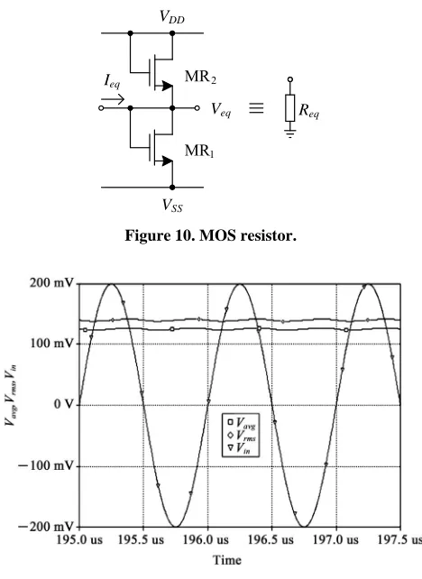
required. For more suitable IC implementation, all grou- nded resistors can be replaced by MOS resistor as shown in Figure 10. This resistor was presented in 1990 by
Wang [14]. Assume MR1 and MR2 have the same
char-acteristics and remaining in the saturation region. The resistance value of MOS resistor can be expressed as:
1
2
eq
DD TH
R
K V V
(9)
where KoCox
W L
, VTH is the threshold voltageand VDD VSS are the supply voltages. It can see that the value of resistor can vary by setting the appropriate aspect ratio.
A first-order low-pass filter is achieved with a prop-erly specified RL and C. The voltage Vout is converted to
the input current of the filter in which the AC compo-nents are filtered through the capacitor C. The voltage
value, Vavg, can be obtained by choosing Rin and RL1
identical. According to (8), Vrms can be obtained by
set-ting RL2/Rin = 1.111. For a symmetrical square input, the
ratio of (8) becomes unity thus Vavg of Figure 9 gives the
exact RMS value because Rin and RL1 are identical. If RL1/Rin = 1.155, the circuit may indicate the RMS value
for either sinusoidal or triangular current signals. The criterion for specifying CL (i.e.CL = CL1 = CL2) is that it
must be large enough to keep the residual output ripple within specified limits, that is [13]
min 1 4π L C f
(10)
where fmin is the low end of the frequency range of
inter-est. CL should usually exceed the right-hand term by the
inverse of the fractional ripple error that can be tolerated at the output [14].
The RMS-to-DC converter in Figure 9 is simulated
using PSPICE program to verify the given theoretical analysis. For this simulation, three resistors (Rin, RL1 and
DDCC1 Y1 X Z Y2 Y3 DDCC2 Y1 X Z Y2
Y3 Vavg
Vrms
Rin
Z
Z
RL1 Vin
Vc
[image:4.595.58.284.70.236.2]CL1 RL2 CL2
[image:4.595.60.290.416.659.2] [image:4.595.62.286.537.661.2] [image:4.595.312.536.556.695.2]RL2) are replaced by MOS resistor as shown in Figure 10
According to (8), when Rin and RL1 are identical to obtain Vav, then Vrms can be obtained by setting RL2/Rin = 1.111.
In this case, the aspect ratios (W/L) of MOS transistors, MR1 and MR2, for Rin, RL1 and RL2 are 2 m/2 m, 2 m/
2 m and 1.8 m/ 2m, respectively (Rin = RL1 = 3.457 k
and RL2 = 3.844 k). A sinusoidal input with Vin = 200 mV
and f = 1 MHz was applied to the converter and C = 1 nF.
The supply voltages for DDCC are selected as VDD =
−VSS = 2.5 V and the bias voltage is set as VB = −1.7 V.
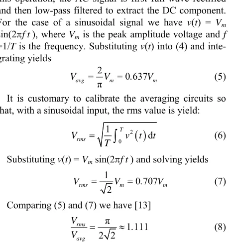
The multiple-output DDCC can be obtained by adding additional current mirrors. Figure 11 shows the
simula-tion results for Vavg = 126.63 mV and Vrms = 140.45 mV,
with ripple less than 2%. In this case, the RMS voltage converter for both sinusoidal (output Vrms) and
symmet-rical square (output Vavg) waveform can be obtained. To
achieve this case, the buffer circuits should be used.
5. Conclusions
In this paper, a new DDCC-based full-wave rectifier has been presented. The proposed circuit comprises only two DDCC which is suitable for IC implementation. The-proposed circuit has high-input and low-output imped-
MR 2
MR 1
VSS Ieq
VDD
Veq Req
[image:5.595.55.289.382.703.2]Figure 10. MOS resistor.
Figure 11. Simulated Vavg and Vrms for sinusoidal input with
amplitude of 200 VPeak and frequency of 1 MHz.
ance terminals, hence it easy to drive loads without using a buffering device. It can be applied to various nonlinear analog signal processing circuits. The performance of the proposed circuit is confirmed from PSPICE simulation results. Simulation results show that the proposed recti-fier have excellent temperature stability. The application of proposed rectifier to pseudo RMS-to-DC conversion is also included.
6. References
[1] J. Peyton and V. Walsh, “Analog Electronics with Op Amps: A Source Book of Practical Circuits,” Cambridge University Press, New York, 1993.
[2] R. G. Irvine, “Operational Amplifier Characteristics and Applications,” Prentice Hall International, Upper Saddle River, 1994.
[3] Z. Wang, “Full-Wave Precision Rectification That is Performed in Current Domain and Very Suitable for CMOS Implementation,” IEEE Transactions on Circuits and Systems-I, Vol. 39, No. 6, 1992, pp. 456-462.
doi:10.1109/81.153637
[4] S. J. G. Gift, “A High-Performance Full-Wave Rectifier Circuit,” International Journal of Electronics, Vol. 89, No. 8, 2000, pp. 467-476.
[5] C. Toumazou, F. J. Lidgey and S. Chattong, “High Fre-quency Current Conveyor Precision Full-Wave Recti-fier,” Electronics Letters, Vol. 30, No. 10, 1994, pp. 745- 746.doi:10.1049/el:19940539
[6] A. Khan, M. A. El-Ela and M. A. Al-Turaigi, “Current- Mode Precision Rectification,” International Journal of Electronics, Vol. 79, No. 6, 1995, pp. 853-859.
doi:10.1080/00207219508926319
[7] K. Hayatleh, S. Porta and F. J. Lidgey, “Temperature Independent Current Conveyor Precision Rectifier,” Elec- tronics Letters, Vol. 30, No. 25, 1995, pp. 2091-2093.
doi:10.1049/el:19941454
[8] A. Monpapassorn, K. Dejhan and F. Cheevasuvit, “A Full- Wave Rectifier Using a Current Conveyor and Current Mirrors,” International Journal of Electronics, Vol. 88, No. 7, 2001, pp. 751-758.
doi:10.1080/00207210110052892
[9] W. Surakumpontorn, K. Anuntahirunrat and V. Riewruja, “Sinusoidal Frequency Doubler and Full-Wave Rectifier Using Translinear Current Conveyor,” Electronics Letters, Vol. 34, No. 22, 1998, pp. 2077-2079.
doi:10.1049/el:19981456
[10] E. Yuce, S. Minaei and O. Cicekoglu, “Full-Wave Recti-fier Realization Using Only Two CCII+S and NMOS Transistors,” International Journal of Electronics, Vol. 93, No. 8, 2006, pp. 533-541.
doi:10.1080/00207210600711606
[11] W. Chiu, S.-I. Liu, H.-W. Tsao and J.-J. Chen, “CMOS Differential Difference Current Conveyors and Their Ap-plications,” IEE Proceeding of Circuits, Devices, System, Vol. 143, No. 2, 1996, pp. 91-96.
[12] S. Minaei and M. A. Ibrahim, “General Configuration for Realizing Current-Mode First-Order All-Pass Filter Using DDCC,” International Journal of Electronics, Vol. 92, No. 6, 2005, pp. 347-356.
doi:10.1080/00207210412331334798
[13] Z. Wang, “Novel Pseudo RMS Current Converter for Sinusoidal Signals Using a CMOS Precision Current
Rectifier,” IEEE Transactions on Instrumentation and Measurement, Vol. 39, No. 4, 1990, pp. 670-671.
doi:10.1109/19.57256
[14] Z. Wang, “2-MOSFET Transistor with Extremely Low Distortion for Output Reaching Supply Voltage,” Elec-tronics Letters, Vol. 26, No. 13, 1990, pp. 951-952.