DOI: 10.4236/jamp.2017.59139 Sep. 15, 2017 1668 Journal of Applied Mathematics and Physics
Semiconductor Failure Analysis
Jacobus Leo, Hao Tan
*, Yinzhe Ma, Shreyas M. Parab, Yamin Huang, Dandan Wang, Lei Zhu,
Jeffrey Lam, Zhihong Mai
GlobalFoundries Singapore Pte. Ltd., Singapore
Abstract
“Industry 4.0” has become the future direction of manufacturing industry. To prepare for this upgrade, it is important to study the automation of semicon-ductor failure analysis. In this paper, the sample polishing activity was studied for upgrading to a smart polishing process. Two major issues were identified in implementing the smart polishing process: the optimization of current po-lishing recipes and the capability of making decisions based on live feedback. With the help of Solver add-in, the current polishing recipes were optimized. To make decisions based on live images captured during polishing, strategies were explored based on finger polishing process study. Our investigation showed that a grey scale line profile analysis on images can be used to build the vision capability of our smart polishing system, on which a decision- making capability can be developed.
Keywords
Semiconductor Process Optimization, Failure Analysis, Image Process, Grey Scale Line Profile Analysis, Smart Polishing System
1. Introduction
Failure analysis (FA) is one of the most important sectors in modern integrated chip (IC) fabrication. Wherever there is a failure limiting production yield or causing chip malfunction, root cause and failure mechanism analysis is needed so as to improve the manufacturing process as well as the product yield. There-fore, FA with high quality is always critical and indispensable for semiconductor industry. Generally, FA on IC chips or wafer pieces can be categorized into physical FA (PFA) and electrical FA (EFA). The former requires layer by layer inspections from top-most layer down to the layer where the defect lies or to the How to cite this paper: Leo, J., Tan, H.,
Ma, Y.Z., Parab, S.M., Huang, Y.M., Wang, D.D., Zhu, L., Lam, J. and Mai, Z.H. (2017) Key Issues for Implementing Smart Po-lishing in Semiconductor Failure Analysis. Journal of Applied Mathematics and Phys-ics, 5, 1668-1677.
https://doi.org/10.4236/jamp.2017.59139
DOI: 10.4236/jamp.2017.59139 1669 Journal of Applied Mathematics and Physics substrate level, with an optical microscope or scanning electron microscope (SEM). The latter, however, includes a lot of special techniques such as na-no-probing, photo emission, thermal analysis by which the suspected failure lo-cation will be isolated for further analysis.
IC chips can be considered as films stacked on silicon substrates. As the defect is usually embedded deep inside the film layers, in most of the cases, a few film layers have to be removed before the defect can be revealed or an EFA can be performed, and this is usually achieved by sample polishing. Obviously, FA quality is directly linked to how well the sample is prepared. The most common method for sample preparation is finger polishing, during which the engineer polishes the sample by pressing it against a rotating platen covered by a certain cloth with slurry supplied in between the sample and the cloth. Finger polishing is simple and flexible, however, its quality is heavily dependent on engineer’s experience.
Since the term “Industry 4.0” emerged in 2011 [1], it has become more and more widely accepted and the manufacturing industry is gradually transforming into “smart factory”. To cope with this trend and get well prepared for the next generation of FA, it is of great urgency to study the automation of all FA tech-niques. In GlobalFoundries Singapore, a prototype smart polishing system with fully automation is currently being built up. Its major hardware consists of a ro-botic arm and a polisher. To implement the smart polishing process, some key issues must be solved. Two major issues we have identified are the optimization of current polishing recipes and the capability of making decisions based on live feedback during polishing. In this paper, optimization on the current finger po-lishing process will be discussed, which will be used for popo-lishing recipe builder programming. Strategies of process and analysis on images obtained from sam-ple polishing will also be discussed, which will lay the foundation for the smart polishing system’s decision making capability.
2. Polishing Process Optimization
2.1. Problem Background
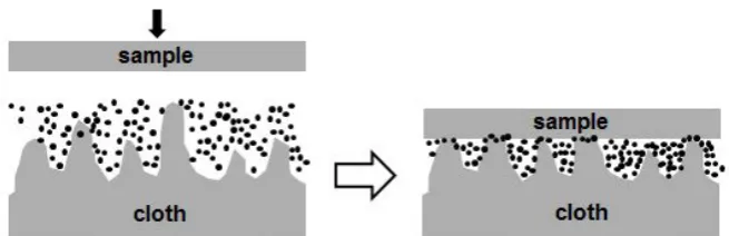
Polishing process is to remove unwanted material away with mechanical forces. Usually, a slurry containing abrasive particles is used to enhance the material removal rate. Moreover, the chemistry of slurry may induce reactions with the sample surface which can help in generating a new layer easily to be peeled off. A simple illustration of polishing process is shown in Figure 1. Before the sample contacts the cloth, the abrasive particles and slurry solution are spread over the polishing cloth.
DOI: 10.4236/jamp.2017.59139 1670 Journal of Applied Mathematics and Physics
Figure 1. Effective abrasive particles in the polishing interface.
affect the material removal rate (MRR). If the force applied is larger, the contact area will increase; however, the increment is not linear and there will be a max-imum value (theoretically will be the sample’s surface area).
MRR can be used to gauge the polishing process. There are several parameters affecting MRR such as pressure or force applied, slurry type (average diameter of the abrasive particles), platen rotation speed and time used. Conventionally, the Preston equation is adopted to predict the MRR [2]:
p
MRR K P V= ⋅ ⋅ . (1)
where P is the force applied, V is the relative velocity and Kp is a general
coeffi-cient which represents the combined effects of the remaining parameters and can be determined experimentally. The Preston equation can only provide a li-near prediction of the variation in the MRR, however, lots of studies have shown that the real MRR during polishing is nonlinear [3]-[11]. In order to simplify our model, we varied the force applied only with three different levels while kept the other parameters fixed. In other words, we only have three different MRR values in our model.
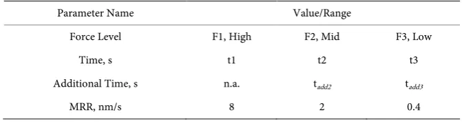
Table 1 lists the MRR at different force level based on experiments.
It can be seen from Table 1 that higher force can bring high MRR value, thus shorter time for the polishing process. However, high force usually brings more scratches to the sample surface which is not preferred as the sample needs to be inspected. Based on experience, once a high force applied, a mid force polishing for 60 s is necessary to undo the possible damages induced by high force polish-ing. The same is true for mid force and in this case, the 60 s low force polishing will be necessary. In order to have the best surface quality, low force polishing for 60s is needed to achieve a smooth surface for inspection.
To avoid unnecessary damages to the target layer, when the high force is ap-plied, it should be stopped when the target layer is 100 nm away. Similarly, for mid force, 50 nm will be the safety distance.
In summary, to achieve high MRR, high force is preferred; however, low force is required for surface quality concern. These two are contradicting with each other and optimization is needed to get the best solution.
2.2. Optimization of Polishing Process by Excel Solver
DOI: 10.4236/jamp.2017.59139 1671 Journal of Applied Mathematics and Physics add-in. Based on the background information above, we have listed the critical parameters for modeling in Table 2, including the MRR values. A set of con-strains based on the requirements are added to the model. Using a global non- linear search method, the Solver can give us the optimized results.
The equations used to build the model in Solver can be expressed as:
Purpose:To find minimum of ( 1 2 3)t t+ +t . (2)
(
2)
(
3)
1 8 2 add 2 3 add 0.4 target thickness to be removed
t ⋅ + t +t ⋅ + t +t ⋅ ≥ (3)
2 0 if 1 0, 2 60 if 1 0
add add
t = t = or t = t ≠ . (4)
3 0 if 2 2 0, or 3 60 if 2 2 0
add add add add
t = t +t = t = t +t ≠ . (5)
3
1, 2, 3 are integers and 1, 2, 3 0, 3t t t t t t ≥ t +tadd ≥60. (6) Equation (3) needs to be adjusted according to real case, as we don’t want to over-polish the sample too much.
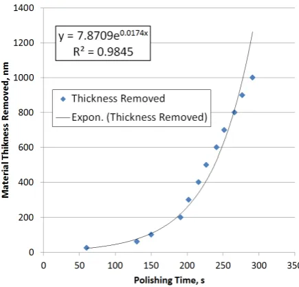
With this model, we can predict the time needed to remove a certain thickness (amount) of material, which is illustrated in Figure 2.
It can be seen clearly from Figure 2 that the relationship between polishing time and removed material thickness is not linear. An exponential fitting was performed by Excel and the fitted equation is shown in Figure 2. The fitting is close to data points, but the variation becomes more and more obvious when the thickness is larger and larger.
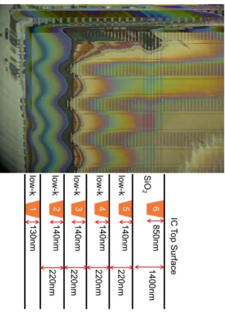
Now let’s use a typical IC device as a real example. The cross-section illustra-tion of a 40nm IC chip with 6 stacking film layers is shown in Figure 3.
Before polishing is started, layer 6 with SiO2 has been removed and only low-k
films left. Usually the last two layers (film 1 and 2 in Figure 3) are important and we normally start inspection from there. The problem now becomes how to re-move three low-k layers efficiently. To include some over-polishing allowance, the total removal thickness is set to be between 580 to 620 nm. Therefore, Equa-tions (2) to (6) can be written as:
Purpose:To find minimum of ( 1 2 3)t t+ +t . (7)
2 3
1 8 ( 2 add ) 2 ( 3 add ) 0.4 580
[image:4.595.204.540.635.728.2]t ⋅ + t +t ⋅ + t +t ⋅ ≥ . (8)
Table 1. Average MRR at different force levels.
Force Level High Mid Low
Average MRR, nm/s 8 2 0.4
Table 2. Parameters for polishing process model.
Parameter Name Value/Range
Force Level F1, High F2, Mid F3, Low
Time, s t1 t2 t3
Additional Time, s n.a. tadd2 tadd3
DOI: 10.4236/jamp.2017.59139 1672 Journal of Applied Mathematics and Physics
[image:5.595.266.484.71.280.2]Figure 2. Predicted polishing time for removing a certain amount of material.
Figure 3. Film stacking structure of a typical 40 nm IC chip.
2 3
1 8 ( 2 add ) 2 ( 3 add ) 0.4 620
t ⋅ + t +t ⋅ + t +t ⋅ ≤ . (9)
2 0 if 1 0, or, 2 60 if 1 0
add add
t = t = t = t ≠ . (10)
3 0 if 2 2 0, or 3 60 if 2 2 0
add add add add
t = t +t = t = t +t ≠ . (11)
3
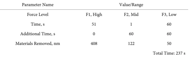
1, 2, 3 are integers and 1, 2, 3 0, 3t t t t t t ≥ t +tadd ≥60. (12) With Equations (7) to (12), we can find solutions with the Solver add-in. Table 3 shows the solution provided by Solver and Table 4 is the recipe cur-rently used by engineers. It can be seen from Table 3 and Table 4 that the po-lishing time has been shortened from 410 s to 237 s, about 42% in reduction. Ve-rification experiments show very good consistence with the prediction.
[image:5.595.303.446.325.489.2]DOI: 10.4236/jamp.2017.59139 1673 Journal of Applied Mathematics and Physics
Table 3. Solution for polishing three low-k layers found by Solver.
Parameter Name Value/Range
Force Level F1, High F2, Mid F3, Low
Time, s 51 1 60
Additional Time, s 0 60 60
[image:6.595.208.540.224.326.2]Materials Removed, nm 408 122 50 Total Time: 237 s
Table 4. Recipe for polishing three low-k layers based on experience.
Parameter Name Value/Range
Force Level F1, High F2, Mid F3, Low
Time, s 30 60 200
Additional Time, s 0 60 60
Materials Removed, nm 240 240 104 Total Time: 410 s
3. Smart Polishing System and Real-Time Decision Making
Strategy
One of the important designed features for the smart polishing system is that it can adjust the polishing parameters based on real-time sample situation. That means, during the polishing process, the system will check the sample’s status and adjust the polishing recipe accordingly.
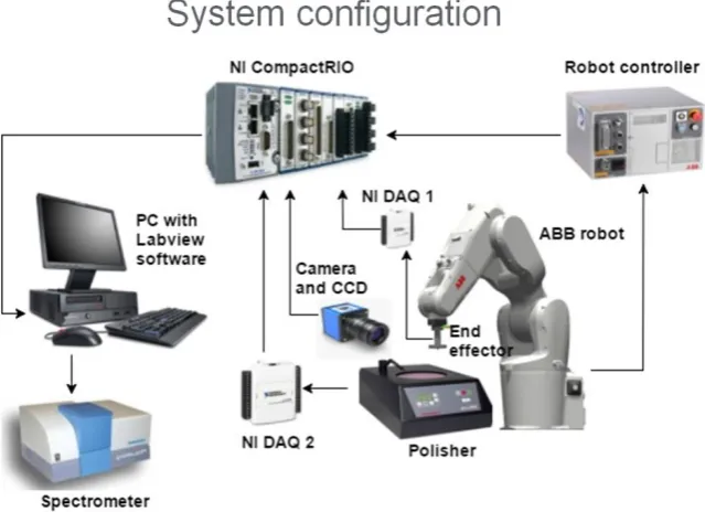
Figure 4 shows the planned configuration of our smart polishing system. The main concept is to use a robotic arm to simulate the finger polishing process. A CCD camera will capture the sample surface status during polishing. Images taken by the camera will be processed and analyzed by our software specially programmed for the system. Based on the live feedback images, the software will evaluate the situation and make decisions for what to do next, so as to ensure the outcome of the polishing process is as expected.
Since the robotic arm is used to simulate finger polishing process, we would like to study how the FA engineer controls the polishing process first and then transfer the learnings to the smart system action designing. One important ac-tion during finger polishing is status check after polishing for a while. Based on the sample surface morphology evolution and pattern recognition, the FA engi-neer can tell if the polishing goal has been achieved. Figure 5 shows the sample surface pattern evolution during finger polishing process. It can be seen from this figure that the pattern is getting irregular with several new features formed after polishing. Our study here is trying to generate useful information from these newly generated features.
DOI: 10.4236/jamp.2017.59139 1674 Journal of Applied Mathematics and Physics
Figure 4. Smart polishing system configuration.
Figure 5. Surface pattern evolution during polishing process.
This phenomenon is not unusual during polishing process and the ripples are related to the IC’s stacking film structure. In fact, we can identify which film the ripple stands for by counting its sequence from the left-most edge (bare silicon surface). To make this clear, we can use the stacking structure in Figure 3 as an example, as illustrated in Figure 6. Please be noted that Figure 3 and Figure 5 are not the same IC chip and only layer 1 and 2 match with the ripples in the current case.
The ripple counting approach stated above is exactly how our FA engineers evaluate the polishing progress. We would like to adopt this ripple identification method to the smart polishing system so the system can evaluate the sample overall situation and find out what to do next, in order to achieve the polishing goal. Obviously this requires lots of image processing and information extraction work, as well as decision-making network to conclude from the information ob-tained. Here, we will explore the image process and the decision-making strate-gies based on the information extracted.
DOI: 10.4236/jamp.2017.59139 1675 Journal of Applied Mathematics and Physics
Figure 6. Relationship between ripples and film stacks.
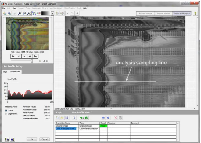
scope changes, we will firstly convert the colored images into grey scale graphs by extracting the color plane information. After that, we will check the grey scale values along a line across the ripples, i.e., line profile check.
Figure 7 illustrates the line profile analysis using NI Vision Assistant. The grey scaled image is under analysis and a sampling line across the ripples is drawn to do the profile check on grey scale values. The small graph at the left bottom corner shows the gray scale value along the sampling line.
If we take a closer look of the line profile graph in Figure 7, several deep val-leys can be seen, which stand for the ripple to ripple interfaces. To make this clearer, the profile graph is aligned with the grey scale image in Figure 8. It can be seen from this figure that the grey scale profile can be used to extract the rip-ple pattern information and each riprip-ple can be correlated to a specific peak on the line profile curve.
DOI: 10.4236/jamp.2017.59139 1676 Journal of Applied Mathematics and Physics
Figure 7. Image processing software interface.
Figure 8. Grey scale line profile and ripple pattern compari-son.
If the sampling line on Figure 7 is drawn at an already known starting point on the chip, the physical coordinates of the IC chip surface will be mapped to the sampling line. Thus the region of interest (ROI) on the sample can be located in the sampling line and the smart polishing system can use this information to judge whether or not the polishing goal (ROI reaches target thickness) has been achieved. Software subroutine based on this strategy is currently being pro-grammed and tested.
[image:9.595.260.488.334.510.2]DOI: 10.4236/jamp.2017.59139 1677 Journal of Applied Mathematics and Physics
4. Conclusions
The implementation of smart polishing requires the integration of a lot of hard-ware parts as well as softhard-ware modules to make it intelligent. There are a lot of important issues which determine the performance of the whole system. We discussed two major issues here for the fundamental study in building up the core functions. The optimization of polishing process demonstrated here can help us to improve the efficiency. Image process and analysis strategy based on grey scale line profile analysis is very promising in realizing the smart system’s vision capability, on which the decision-making capability based on live feed-back can be developed.
References
[1] Grillo, G. Wikipedia, Industry 4.0. https://en.wikipedia.org/wiki/Industry_4.0
[2] Preston, F.W. (1927) The Theory and Design of Plate Glass Polishing Machines.
Journal of the Society of Glass Technology, 11, 214-256.
[3] Seo, J., Moon, J., Kim, Y., Kim, K., Lee, K., Cho, Y., Lee, D.H. and Paik, U. (2017) Synergistic Effect of mixed Particle Size on W CMP Process: Optimization Using Experimental Design. ECS Journal of Solid State Science and Technology, 6, 42-44.
https://doi.org/10.1149/2.0171701jss
[4] Singh, A., Garg, H., Kumar, P. and Lall, A.K. (2017) Analysis and Optimization of Parameters in Optical Polishing of Large Diameter BK7 Flat Components. Materials and Manufacturing Processes, 32, 542-548.
https://doi.org/10.1080/10426914.2016.1221103
[5] Fang, C., Zhao, Z.X., Lu, L.Y. and Lin, Y.F. (2017) Influence of Fixed Abrasive Con-figuration on the Polishing Process of Silicon Wafers. International Journal of Ad-vanced Manufacturing Technology, 88, 575-584.
https://doi.org/10.1007/s00170-016-8808-9
[6] Zhang, K.L., Feng, Y.L., Cao, J., Wang, F., Han, Y.M., Yuan, Y.J. and Wong, H.S. (2014) Optimization and Mechanism on Chemical Mechanical Planarization of Hafnium Oxide for RRAM Devices. ECS Journal of Solid State Science and Tech-nology, 3, 249-252. https://doi.org/10.1149/2.0131407jss
[7] Wang, T.Q., Lu, X.C., Zhao, D.W., He, Y.Y. and Luo, J.B. (2013) Optimization of Design of Experiment for Chemical Mechanical Polishing of a 12-Inch Wafer. Mi-croelectronic Engineering, 112, 5-9. https://doi.org/10.1016/j.mee.2013.05.010
[8] Jeng, Y. and Huang, P. (2005) A Material Removal Rate Model Considering Interfa-cial Micro-Contact Wear Behavior for Chemical mechanical Polishing. Transac-tions of the ASME, 127, 190-197. https://doi.org/10.1115/1.1828068
[9] Wang, T.Q., Zhao, D.W., He, Y.Y. and Lu, X.C. (2013) Effect of Slurry Injection Po-sition on Material Removal in Chemical Mechanical Planarization. International Journal of Advanced Manufacturing Technology, 67, 2903-2908.
https://doi.org/10.1007/s00170-012-4702-2
[10] Jeng, Y.R. and Tsai, H.H. (2003) Improved Model of Wafer/Pad Powder Slurry for CMP. Journal of the Electrochemical Society, 150, G348-G354.
https://doi.org/10.1149/1.1572485
[11] Jeng, Y.R., Huang, P.Y. and Pan, W.C. (2003) Tribological Analysis of CMP with Partial Asperity Contact. Journal of the Electrochemical Society, 150, G630-G637.
Fair and swift peer-review system
Efficient typesetting and proofreading procedure
Display of the result of downloads and visits, as well as the number of cited articles Maximum dissemination of your research work
Submit your manuscript at: http://papersubmission.scirp.org/