Crystallization Behaviour of Electroless Ni-P UBM with Medium Phosphorous
Induced by Single and Step Heat Treatment
Han-Byul Kang
1;2, Jongwoo Park
2, Jee-Hwan Bae
1and Cheol-Woong Yang
1;* 1School of Adv. Material Sci. & Eng., Sungkyunkwan University, Suwon 440-746, Korea
2Technology Reliability, System LSI, Samsung Electronics, Yongin 446-711, Korea
This study examined the crystallization behavior of electroless Ni-P UBM with an medium phosphorous content (15at%) induced by a single and step heat treatment usingin-situtransmission electron microscopy (TEM). Different heat treatment processes affected the crystallization behavior of electroless Ni-P UBM. After single heat treatment at 300C for 60 min, the electroless Ni-P UBM contained Ni and
Ni3P. In addition to Ni and Ni3P, more complex Ni-P compounds, such as Ni12P5and Ni5P2formed in the electroless Ni-P UBM resulting from a step heat treatment at 150C for 60 min followed by 300C for 60 min. [doi:10.2320/matertrans.M2010178]
(Received May 20, 2010; Accepted July 5, 2010; Published August 19, 2010)
Keywords: under bump metallization, electroless nickel-phosphorous, in-situ transmission electron microscopy (TEM)
1. Introduction
In flip chip interconnections using a solder bump, under bump metallization (UBM) is desirable because the solder cannot be bonded directly to the Al or Cu pads. Therefore, electroless Ni-P (EN-P) UBM has attracted considerable attention for flip chip bumping technology on account of its simple process, low cost, good solder wettability, bump uniformity and superior diffusion barrier performance.1–5)
EN-P films can be classified into three categories with respect to the microstructural differences as a function of the phosphorus content; phosphorus supersaturated structure
with a low phosphorous content (<7at%), compounded
nanocrystalline Ni and amorphous structure with a medium
phosphorous content (819at%), and fully amorphous
structure with a high phosphorous content (>20at%).6–9)
the thermo-mechanical and/or physical properties of EN-P UBM depend on the microstructural characteristics, which are governed and determined by the crystallization behavior during post heat treatment, such as the reflow and aging process. It was reported that the formation of crystalline Ni-P phases is quite sensitive to the heat treatment, and their mechanical properties can be reversed when exposed to an
overheating temperature and improper dwelling time.10,11)
Therefore, it is important to understand the crystallization behavior of EN-P UBM as a function of the heat treatment and profile. Many studies characterized the crystallization behavior of EN-P films with different phosphorous contents under a single heat treatment.12–18)However, few studies are
available. Moreover, the effects of the post heat profile, e.g. a single and step heat treatment, on the crystallization behavior of EN-P films with respect to the phosphorous content are not completely understood. Therefore, a systematic well charac-terized physical study is essential for understanding the crystallization behavior of EN-P UBM.
This study examined the crystallization behavior of the amorphous EN-P UBM with a medium phosphorous content (15 at%) as a function of the heat profile consisting of a single
(300C/60 min) and step (150C/60 min followed by 300C/
60 min) heat treatment. One of the aims was to characterize the crystallization behavior of EN-P with a medium
phosphorous content using in-situ transmission electron
microscopy (TEM), which can provide a better understand-ing of the microstructural behavior and the mechanism evolved.
2. Experimental Procedure
Copper foil was used as the substrate in EN-P plating. A commercially available EN-P plating solution (ICP Nicoron GIB series, Okuno Chemical Industries Co., Ltd., Japan) was
used for EN-P plating. The EN-P plated layer with a15at%
phosphorous content was processed at 90C for 30 min. After
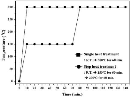
plating, the sample was heat treated in a tube furnace with an argon atmosphere. Figure 1 shows the temperature profile of a single (300C/60 min) and step (150C/60 min followed by
300C/60 min) heat treatment. The microstructure of EN-P
UBM as-plated and after heat treatment was analyzed by X-ray diffraction (XRD, Rigaku, Japan) and TEM. The XRD patterns of the sample after the heating processes were recorded at room temperatures. The TEM samples were prepared using an ultramicrotome (RMC MT 7000) and characterized by high resolution (HR)-TEM (JEM-2100F,
Fig. 1 Heat profile of a single and step heat treatment.
[image:1.595.318.534.301.463.2]Jeol Co. Ltd.) equipped with a scanning transmission electron microscope (STEM) and energy dispersive x-ray spectrom-eter (EDS). A JEOL 3011 TEM equipped with a hot stage
was used for thein-situTEM studies.
3. Results and Discussion
3.1 XRD analysis after single and step heat treatment
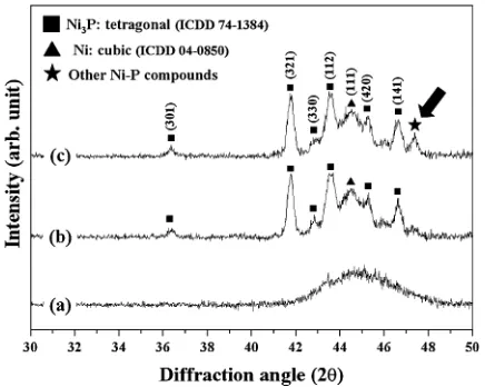
Figure 2 shows XRD patterns of the as-plated EN-P and post heat treated films. As shown in Fig. 2(a), the XRD patterns of the as-plated sample before heat treatment
revealed a single broad peak at 45 2, which indicates an
amorphous structure. Several sharp peaks were observed on the XRD patterns when EN-P UBM was exposed to a single
heat treatment at 300C/60 min [see Fig. 2.(b)]. Two
crystalline peaks, Ni and Ni3P, were noted on the XRD
patterns, showing that both Ni and Ni3P form in EN-P UBM
during a single heat treatment. Figure 2(c) presents the XRD
patterns of a step heat treated EN-P film, 150C/60 min
followed by 300C/60 min. Ni and Ni
3P peaks were observed on the XRD pattern, which is similar to that of the single step heat treated EN-P UBM. In addition, the XRD pattern of the
step treated EN-P UBM showed a new sharp peak at47:38
2 corresponding to the (240) Ni12P5 (46.96 2) or (600)
Ni5P2 (47.64 2) peak. Various Ni-P compounds can be
formed in EN-P UBM with a medium phosphorous, particularly those treated at intermediate temperatures (150C) using a step heat profile. It should be noted that a
single heat profile at 300C/60 min provides Ni and Ni
3P as
the main precipitates.
Amorphous EN-P is thermo-dynamically unstable and transforms to more stable structures during heat treatment. Many studies of the crystallization behavior of EN-P films reported that crystallized Ni-P phases are sensitive to the
phosphorus content in the EN-P film.9,12–16) In the case of
a low (<79at%) and medium (918at%) phosphorous
content, the Ni-P compound precipitate is dominated by Ni3P.6,16,18) However, at high phosphorous contents (>20at%), Ni3P and NixPycompounds, such as Ni2P, Ni5P2 and Ni12P5, form after heat treatment.12,13,16) And the transformation from the amorphous Ni-P to the crystalline
equilibrium two-phase mixture of Ni and Ni3P occurred
through the crystallization of the intermediate meta-stable
mixture of NixPy and Ni in accordance with the Ostwald
rule.19) Surprisingly, the medium phosphorous (15 at%) in
the EN-P UBM processed by a step heat treatment yielded similar results to those observed with a high phosphorous content (>20at%) reported in literatures. Therefore, the given heat profile for EN-P UBM plays an important role in the crystallization behavior.
3.2 In-situTEM analysis during step heat treatment
In-situ TEM was employed to determine the reason for the unexpected crystallization behavior of the EN-P with the medium phosphorous (15 at%) induced by a step heat
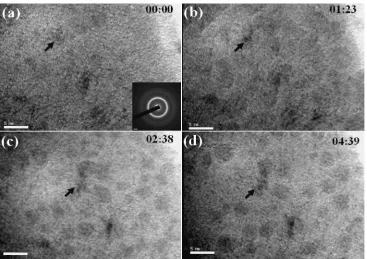
treatment. Figure 3 shows the in-situTEM image sequence
during heat treatment at an intermediate temperature
(150C). As shown in the selected area diffraction (SAD)
pattern in Fig. 3(a), the as-plated EN-P UBM exhibited diffused halo rings, which suggests an amorphous structure. However, the dark spots become more apparent, and they grow in size with increasing heat treatment duration (see
Fig. 3(b)(d)). Given that the dark spots indicate
nano-crystalline Ni. Figure 4 shows the results of ex-situ TEM
analyses on the EN-P UBM exposed to 150C for 60 min. As
shown in the diffraction pattern in Fig. 4(a), the d-spacing measured from the Debye rings apparently represents crystalline Ni. This shows that crystallized Ni exists in the
amorphous EN-P UBM even after heat treatment at 150C.
Furthermore, Table 1 shows the results of STEM/EDS analyses on the EN-P heat treated at 150C in a step profile. The changes in Ni and P are obvious, which is well matched
with the in-situ TEM results. The dark area contained
92at% Ni and 8at% P (position 14 in Fig. 4(b)),
suggesting that it is Ni rich. However, the phosphorous
content increased up to 23 at% in positions 58 shown in
Fig. 4(b), this suggests that P was segregated at the region between the Ni rich regions, and the P concentration can increase to more than 15 at% after heat treatment at
intermediate temperatures (150C). It was assumed that the
change in Ni and P composition governed by a step heat treatment can result in a more complicated crystallization behavior of the EN-P UBM with a medium phosphorous content (15at%). These results are discussed in the later parts.
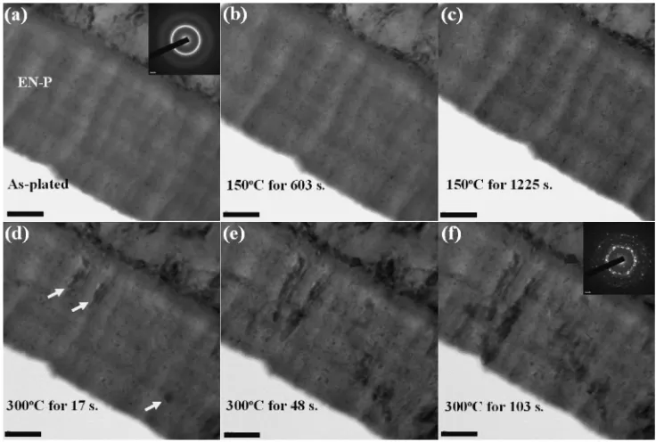
Figure 5 shows in-situ TEM images during a step heat
treatment at 150C/60 min followed by 300C/60 min. As
shown in Fig. 5(a), several dark spots (11:5nm) were
observed on the as-plated EN-P UBM. Since the EN-P film contains15at% phosphorous, it is reasonable that the EN-P consists of nanocrystalline Ni and amorphous EN-P, which is consistent with previous studies.13,16,17)In an earlier stage of
heat treatment at 150C, the dark spots (Ni) became clearer in
shape and increased in size with increasing dwelling time (see Fig. 5(b) and (c)). These results are similar to thein-situ TEM analyses shown in Fig. 3. The crystallization of Ni-P
compounds was observed as the temperature reached 300C.
In turn, Ni-P crystallization occurs rapidly after 100
seconds. As shown in Fig. 5(f), the diffraction pattern of the EN-P UBM consisted of a Debye ring superimposed with diffraction spots, which supports the crystallized Ni-P Fig. 2 XRD patterns of the plated EN-P and heat-treated films: (a)
as-plated ENP UBM, (b) a single heat treatment (300C/60 min) and (c) a
[image:2.595.60.278.71.245.2]compounds formed in the EN-P UBM. Nano-beam-electron-diffraction (NBED) was used to identify the crystalline phases in the EN-P UBM after a step heat treatment. Figure 6 shows the results of NBED analyses on the samples exposed to a step heat treated EN-P UBM shown in Fig. 5(f). NBED confirmed that crystallized EN-P UBM consisted of a mixture of Ni3P, Ni12P5, Ni5P2and Ni. Figure 6 shows that the indexed NBED patterns of Ni3P, Ni12P5, Ni5P2 and Ni
with the zone axis of [1101], [1122], [001] and [011],
respectively. Few studies have reported the similar results. Pittermann and Ripper using high energy electron diffraction confirmed the existence of a meta-stable Ni5P2 or Ni2:55P structure prior to the formation of the stable Ni3P (P content
between 15 and 25 at%).20) Maeda found that higher Ni-P
compounds such as Ni5P4 and Ni7P3, in addition to Ni3P, exist in the films containing less than 12 at%.21) This also Fig. 4 TEM results of the EN-P UBM after the heat treatment at 150C for 60 min. Note that position14consists of92at% Ni and
[image:3.595.116.483.70.329.2]8at% P, and position58indicates phosphorous up to 23 at%.
Table 1 The results of quantitative STEM/EDS analyses on the heat treated EN-P UBM at 150C for 60 min.
Position Ni (at%) P (at%)
1 91:731:13 18:271:01
2 92:640:93 17:360:71
3 92:910:85 17:090:69
4 92:251:09 17:750:93
5 76:310:84 23:690:97
6 76:101:08 23:901:20
7 75:561:32 24:441:55
8 76:170:95 23:831:02
Fig. 3 In-situTEM images during heat treatment at an intermediate temperature at 150C: As the heat treatment duration increases, dark
[image:3.595.115.486.387.549.2] [image:3.595.46.290.659.786.2]confirmed that various Ni-P compounds formed in the EN-P UBM with a medium phosphorous content (15 at%) are due primarily to a step heat treatment. And these results are the systematically work presenting the crystallization process of high P compound in the films containing medium P (15 at%).
3.3 Crystallization behaviors of the EN-P with the medium phosphorous
Many studies reported the crystallization behavior of
medium P containing EN-P films.6,12,13,16,17) They claimed
that a heat treated EN-P film with a medium P consists of
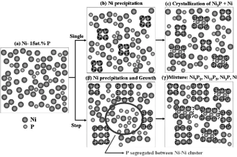
crystallized Ni and Ni3P. Figure 7 shows a schematic
diagram of the crystallization behavior of EN-P with 15 at% phosphorous. Heat treatment enhanced structural relaxation of the as-plated EN-P film. The rate of Ni diffusion was relatively faster than that of phosphorous. Therefore, the
size of the Ni-Ni clusters increased during heat treatment, such that the precipitation of nanocrystalline Ni in the EN-P
film develops (Fig. 7(a)!(b)). At higher temperatures, a
stable microstructure of a mixture of Ni3P and Ni can be
formed as a result of recrystallization (Fig. 7(b)!(c)),13,16,18)
which agrees with the results taken from a single heat treatment (see Fig. 2(b)). As shown in previous TEM analyses in Figs. 3 and 4, the size of the Ni-Ni cluster continues to grow in an intermediate temperature of the step heat profile.22)At the region between the Ni rich area with a
phosphorous concentration of 23at%, the crystallization
behavior is similar to that of EN-P with a high phosphorous content (>20at%). In addition to Ni3P and Ni, other Ni-P compounds formed, such as Ni12P5and Ni5P2, resulting from a step heat treatment. Therefore, the crystallization process of EN-P with a medium phosphorous content induced by the Fig. 5 In-situTEM images taken from the step heat treatment (150C followed by 300C): (a) as-plated EN-P, (b)(c) at 150C, and
(d)(f) at 300C. The scale bar shown in TEM images is 50 nm.
[image:4.595.113.481.72.320.2] [image:4.595.115.482.369.546.2]step heat profile can be described as follows: structural
relaxation! Ni precipitation!phosphorous segregation
between a Ni-Ni cluster at an intermediate temperature (Fig. 7(a)!())!mixture of Ni5P2, Ni12P5, Ni3P and Ni (Fig. 7()!()). Again, a step heat treatment of the EN-P with a medium phosphorous content contributes to the formation of a range of Ni-P compounds.
4. Conclusions
XRD andin-situTEM were used to examine the effects of
different heat profiles on the crystallization behavior of EN-P UBM with a medium phosphorous content. A single heat
treatment of the EN-P UBM at 300C/60 min yielded Ni and
Ni3P as the primary precipitates. The step heat profile of
150C/60 min followed by 300C/60 min enabled the
growth of more complex crystalline Ni-P compounds in the formation of Ni3P, Ni12P5, Ni5P2 and Ni. Different heat treatment processes can affect the crystallization behavior of electroless Ni-P UBM.
Acknowledgments
The authors would like to thank for financial supports from the Korea Science and Engineering Foundation (KOSEF) grant funded by the Korea government (MEST, No. 2009-0060183) and Brain Korea 21 program.
REFERENCES
1) J. Simon, E. Zakel and H. Reich: Proc. 40th Electronic Components and Technology Conference, (New York, 1990) pp. 412.
2) K. Zeng and K. N. Tu: Mater. Sci. Eng. R.38(2002) 55. 3) J. W. Yoon and S. B. Jung: Surf. Coat. Tech.200(2006) 4440. 4) H. B. Kang, J. W. Lee, J. H. Bae, M. H. Park, J. W. Yoon, S. B. Jung,
J. S. Ju and C. W. Yang: J. Mater. Res.23(2008) 2195.
5) H. B. Kang, J. H. Bae, J. W. Lee, M. H. Park, J. W. Yoon, S. B. Jung and C. W. Yang: J. Electron. Mater.37(2008) 84.
6) J. W. Yoon, H. S. Chun, H. B. Kang, M. H. Park, C. W. Yang, H. J. Lee and S. B. Jung: Surf. Rev. Lett.14(2007) 827.
7) A. H. Graham, R. W. Lindsay and H. J. Read: J. Electrochem. Soc.112 (1965) 401.
8) N. M. Martyak: Chem. Mater.6(1994) 1667.
9) P. S. Kumar and P. K. Nair: J. Mater. Process. Technol.56(1996) 511. 10) M. H. Staia, E. S. Puchi, G. Castro, F. O. Ramirez and D. B. Lewis:
Thin Solid Film355(1999) 472.
11) H. Pfeiffer, F. Tancret and T. Brousse: Mater. Chem. Phys.92(2005) 534.
12) E. Ma, S. Luo and P. Li: Thin Solid Film166(1988) 273. 13) K. Hur, J. Jeong and D. Lee: J. Mater. Sci.25(1990) 2573. 14) G. W. Marshall, D. B. Lewis and B. E. Dodds: Surf. Coat. Technol.53
(1992) 223.
15) D. Tachev, J. Georgieva and S. Armyanov: Electrochim. Acta 47 (2001) 359.
16) J. Gao, Y. Wu, L. Liu, B. Shen and W. Hu: Mater. Lett.59(2005) 1665. 17) TH. Hentschel, D. Isheimi, R. Kirchheimi, F. Mueller and H. Kreye:
Acta Mater.48(2000) 933.
18) H. S. Yu, S. F. Luo and Y. R. Wang: Surf. Coat. Technol.148(2001) 143.
19) E. Vafaei-Makhsoos: J. Appl. Physics51(1980) 6366. 20) U. Pittermann and S. Ripper: Z. Metallkde.74(1983) 783. 21) H. Maeda: Trans. National Res. Inst. Metals12(1970) 211. 22) H. B. Kang, J. H. Bae, J. W. Lee, M. H. Park, Y. C. Lee, J. W. Yoon,
S. B. Jung and C. W. Yang: Scr. Mater.60(2009) 257. Fig. 7 Schematic diagram of crystallization behaviors of the EN-P with the
[image:5.595.48.288.72.231.2]