Dynamics of electronic transitions and frequency dependence of negative capacitance
in semiconductor diodes under high forward bias
Kanika Bansal, Mohamed Henini, Marzook S. Alshammari, and Shouvik Datta
Citation: Applied Physics Letters 105, 123503 (2014); doi: 10.1063/1.4896541
View online: http://dx.doi.org/10.1063/1.4896541
View Table of Contents: http://scitation.aip.org/content/aip/journal/apl/105/12?ver=pdfcov
Published by the AIP Publishing
Articles you may be interested in
Analysis of carrier transport and carrier trapping in organic diodes with
polyimide-6,13-Bis(triisopropylsilylethynyl)pentacene double-layer by charge modulation spectroscopy and optical second harmonic generation measurement
Appl. Phys. Lett. 105, 073301 (2014); 10.1063/1.4893760
Electroluminescence and capacitance-voltage characteristics of single-crystal n-type AlN (0001)/p-type diamond (111) heterojunction diodes
Appl. Phys. Lett. 98, 011908 (2011); 10.1063/1.3533380
Temperature-dependent transition from injection-limited to space-charge-limited current in metal-organic diodes Appl. Phys. Lett. 95, 143303 (2009); 10.1063/1.3243844
Capacitance-voltage characterization of polyfluorene-based metal-insulator-semiconductor diodes Appl. Phys. Lett. 89, 013506 (2006); 10.1063/1.2219147
Dynamics of electronic transitions and frequency dependence of negative
capacitance in semiconductor diodes under high forward bias
Kanika Bansal,1Mohamed Henini,2Marzook S. Alshammari,3and Shouvik Datta1
1
Division of Physics, Indian Institute of Science Education and Research, Pune 411008, Maharashtra, India
2
Nottingham Nanotechnology and Nanoscience Centre, School of Physics and Astronomy, University of Nottingham, Nottingham NG7 2RD, United Kingdom
3
The National Center of Nanotechnology, KACST, Riyadh 11442, Saudi Arabia
(Received 20 June 2014; accepted 14 September 2014; published online 24 September 2014)
We observed qualitatively dissimilar frequency dependence of negative capacitance under high charge injection in two sets of functionally different junction diodes: III-V based light emitting and Si-based non-light emitting diodes. Using an advanced approach based on bias activated differential capacitance, we developed a generalized understanding of negative capacitance phenomenon which can be extended to any diode based device structure. We explained the observations as the mutual competition of fast and slow electronic transition rates which are different in different devices. This study can be useful in understanding the interfacial effects in semiconductor heterostructures and may lead to superior device functionality.VC 2014 AIP Publishing LLC.
[http://dx.doi.org/10.1063/1.4896541]
Even after decades of research in the field of semicon-ductors, behavior of a semiconductor junction diode under high forward bias is not fully understood. Junction diodes make the basis of a vast variety of devices which are an inte-gral part of technology and consumers applications. Some of these diodes, such as light emitting diodes (LED) and laser diodes (LD), can function only under high forward bias. Hence, it becomes important to understand the electrical impedance of these diodes under such high forward bias not only to gain knowledge about the physical processes they undergo but also to make them more useful in various appli-cations. In our previous studies,1–4 we investigated the impedance of electroluminescent diodes (LEDs and LDs) under charge carrier injection. We observed that as the forward bias increases, the reactive component of the imped-ance demonstrates negative capacitimped-ance (NC). Higher mag-nitude of this NC for lower applied modulation frequencies has also been observed by many groups in electrolumines-cent devices5–7and also in other semiconductor devices.8,9
Here, we report qualitatively opposite dynamic behavior of NC in two sets of diodes with different functionalities: (a) III-V based electroluminescent diodes (ELDs): (i) InGaAs based quantum dot laser (QDL) diodes grown by Molecular Beam Epitaxy (MBE) on (100) GaAs substrates. A 0.7l m-thick GaAs buffer layer was grown before deposition of the In0.5Ga0.5As strained layer at 450C. The structure was
com-pleted with a 25 nm GaAs cap. Further details can be found in Ref. 10. (ii) Commercially purchased AlGaInP based quantum well laser (QWL) diodes from Sanyo (component No. DL 3148–025). These are edge emitting strained multi-quantum well structures (details can be found in Ref. 1), and (b) Si-based non-luminescent diodes: commercially purchased standard Si-based diodes 1N 4001, 1N 4007, and p-i-n photo diode SFH 213 from OSRAM Opto Semiconductors. The modulation frequency dependence of negative capacitance in Si diodes was found to be different than that of ELDs. We developed the analysis based on the frequency derivative of capacitance to probe such difference.
We came up with a generalized understanding of negative capacitance as a mutual competition of two rate-limited processes to explain the observations.
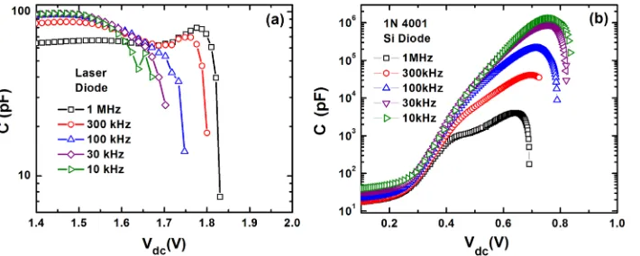
Figure 1(a) shows variation of measured small signal capacitance (C, using precision LCR meter E4980A from Agilent) with forward bias for QWL at different modulation frequencies. As the bias (Vdc) increases, the capacitance
becomes negative and in the log scale, the frequency response curve terminates. With lower applied modulation frequency, the onset of negative capacitance occurs at lower forward biases. On the other hand, Figure 1(b) shows such capacitance voltage plots for Si diode (1N 4001) under for-ward bias. Frequency dependence of negative capacitance is completely reversed in this case. As the frequency decreases, we observe negative capacitance onset to shift towards higher applied injection levels. We also measured such nega-tive capacitances in other Si based diodes (p-i-n photo diode SFH 213 and 1N 4007), all of which gave qualitatively similar frequency dependence.
In our earlier studies,1,2 to explain the occurrence of negative capacitance in ELDs, we considered the mutual competitive dynamics of sub-band gap defect levels and radiative recombination of available charge reservoir at high injection levels. Depending upon the applied modu-lation frequency and temperature of the device, defects within a certain energy depth ETh can respond1 to the
applied signal and contribute to the measured impedance. Hence, one can write the standard expression relating ETh, thermal rate of charge carriers trapping and
de-trapping from defect states (s), and modulation frequency (f) as
f 1
s¼exp ETh
kBT
(1a)
or
where T is the temperature which we kept constant (29660.1 K) during the measurements,kBis the Boltzmann
constant, and is the thermal prefactor. When the applied modulation is comparable to 1/s, we observe that the defect responds to the applied sinusoidal modulation which ultimately affects the measured impedance of the active junction.
In case of ELDs, the onset of light emission also inter-rupts the total number of charge carriers available at the junction which includes the contribution from defect levels (nTrapped). Radiative recombination process consumes charge
carriers coming out of the defect states irreversibly and faster than these are replenished. As a result, at the end of the mod-ulation cycle, equilibrium defect popmod-ulation is not recovered. This can cause a transient change in the quasi Fermi level position and the carrier reservoir at the junction. To establish the equilibrium, a compensatory current is induced which lags behind the voltage. Consequently, we observe an “inductive like” reactance, experimentally measured as NC. The more is the contribution from defect levels (nTrapped),
the more compensation would be required to achieve such equilibrium. It is easy to understand from Eq.(1)that with decreasing frequency,EThincreases. This increases nTrapped
and hence the magnitude of compensatory current which ultimately increases the magnitude of NC at decreasing mod-ulation frequencies, as observed in the past.1,2
However, in case of non-luminescent Si-based diodes, such fast (ps) radiative recombinations do not take place. Yet the occurrence of NC points towards the presence of mutually competing different rate-limited electronic proc-esses with different time scales.
To further examine the dynamic dependence of NC on frequency, in Figure2, we plot and compare the bias values
at which the NC starts to occur (VNC) as a function of
fre-quency ffor two different types of diodes. In case of ELDs (Figure 2(a)), VNCincreases monotonically with increasing
applied frequency. This behavior remains qualitatively the same for QWL and QDL diodes and is in accordance with the results reported by Feng et al.11 It is important to note that the defect contribution can only be activated if defects exist below the quasi Fermi level in the band gap.1 As we increase frequency, we decrease the depthETh, and hence the
contribution from relatively deeper defects is lost. To over-come this, quasi Fermi level has to move towards the band edge to increase the effective defect contribution, which can be achieved by increasing the applied bias (at a constant temperature). Once the defect contribution is significant to compete with the radiative recombination process, we start observing NC. This is why we observe that as the modulation frequency increases, VNCincreases in ELDs.1
On the other hand, as shown in Figure2(b), for all the Si based non-luminescent devices investigated, VNC does not
follow a monotonic behavior with increasing f. Here, two different regions can be clearly identified depending upon the variation of VNCwith frequency. In region I, VNCis
rela-tively independent of applied modulation frequencies for lower frequency ranges below 5104Hz and remains relatively constant. In region II, above 5104Hz, VNC
decreases with increasing frequencies which is opposite of what is observed in the case of ELDs.
[image:3.612.53.408.53.195.2]To understand this difference, we studied the frequency derivative of capacitance response. Usually, a peak infdC/df is observed with frequency or temperature variation corre-sponding to a position of maximum response from the defects or the position where quasi Fermi level crosses the respective defect energy level.12–14 In case of high charge FIG. 1. Variation of capacitance with bias under different applied modula-tion frequencies for (a) quantum well laser diode (DL 3148-025) and (b) Si diode (1N 4001). The point where a particular data plot terminates is the starting point of negative capacitance. In Si diodes, high frequency produces negative capacitance for lower biases which is opposite to that of quantum well laser diodes.
FIG. 2. Variation of the bias at which negative capacitance is observed (VNC) for different applied modulation
frequencies for (a) QWL and QDL diodes and (b) Si based diodes. For laser diodes, VNCincreases
monotoni-cally with increasing frequency. For Si diodes, VNCfirst stays somewhat
con-stant with increasing frequency range (region I) and then decreases with increasing frequencies (region II).
[image:3.612.52.418.626.771.2]injection, which induces interesting NC behavior, we focus on the bias (Vdc) activated dynamics of rate processes at
room temperature. Experiments show that4this dependence of rate process on T and Vdc is mutually inverse and is
expressed as 1/T¼gVdc, where g is a proportionality
con-stant for correct dimensionality. Equation (1) can then be modified to the form
fMaxexp
ETh
kB
gVdc
; (2)
where fMax corresponds to the frequency of maximum
response (in fdC/df vs f plot). Rewriting Eq. (2) gives
lnfMax¼lnþ EkThB gVdc
. To verify the validity of this
equation, linear behavior of lnfMax with Vdc is required,
which we have demonstrated in case of ELDs.4 Thus, the slope (m) of the straight line is directly proportional to the thermal activation energy, i.e.,
m¼ ETh
kB
g
: (3)
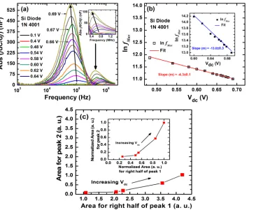
Figure 3(a) shows the variation of fdC/df for a wide range of applied modulation frequencies for Si diode 1N 4001. We observe two prominent peaks in the fdC/df vs f plot. This is fundamentally different from the differential capacitance response observed in case of ELDs, where only one peak was observed.4As the bias increases,fMaxfor both
the peaks shifts to the respective lower frequency sides. This variation of lnfMax with applied bias is plotted in
Figure 3(b). Such linear variation of ln fMax with Vdc
validates our conceived equation(2). Values of the slopes are found to be 4.360.1 for lower frequency and
13.060.3 for higher frequency response. This difference may be related to entropic contribution to free energy bar-rier for a particular electronic defect.15 Unlike ELDs,4 Si based diode structures do not show any sign change of slopes in lnfMaxvs Vdcplot, which were related to the
pres-ence of excitons during light emission. It is worth mention-ing that the behavior of undifferentiated capacitance with frequency, as shown in Ref. 16, Figure S1 (supplementary material) matches well with the previously reported results on Si based photodetectors.17Though the occurrence of NC is shown in that report, the frequency dependence has not been dealt with. In this letter, we elaborate on this less explored feature of NC for commonly available diodes, which otherwise show similar properties as per reported literature, by using the advanced technique and analyses we have developed.
Note that in these bias activated processes, as the modu-lation frequency reaches between5104and 106Hz, peak 2 starts to respond significantly only after 0.45 V. However, slower defect response (peak 1) starts appearing at much lower biases. The density of defects responding at such fre-quencies is directly proportional to the derivativefdC/df.12,15 Hence, the area under the peaks represents the density of defects within the energy range spanned by the correspond-ing range of modulation frequency. In Figure3(c), we found that the area acquired by the right half of peak 1 (overlapping with peak 2) increases in correlation with the area acquired by peak 2. Net defect density of peak 1 is much larger as compared to peak 2. However, at large forward biases, the rate of increase in peak 2 is faster than that of peak 1. This can be viewed from the plot in the inset of Figure3(c), where values are normalized with respect to the highest area value for respective peaks. We ascribe this observed correlation as
FIG. 3. (a) Absolute value offdC/df
showing two peaks at different fre-quency positions for Si diode. Peak frequency values are used to plot lnfMaxwith applied bias (Vdc) as shown
[image:4.612.55.421.470.771.2]an evidence for competition of two rate-limited processes governing the voltage onset of NC.
In Si diodes, two differently sized defect responses (big-ger peak 1 and smaller peak 2) overlap (within similar fre-quency/energy ranges) and compete with each other for the overall impedance of the junction. At modulation frequen-cies >5104 Hz, the steady state situation is not fully recovered at the end of the sinusoidal modulation because the presence of a dominant and slower defect channel inter-rupts the dynamics of relatively smaller but faster defect response. This results in a mismatch of charge trapping and emission from these two defect channels over a complete cycle. Subsequently, a transient change in the charge carrier population coming from these defects can surface, giving rise to a compensatory current and hence the negative capac-itance.1,2 In this region II of Figure 2(b), the contribution from relatively faster defect channels reduces with decreas-ing frequency. This requires further increase in the applied bias to generate significant contribution from shallower and faster channels which compete with slower channels to pro-duce NC. As a result, VNC increases with decreasing
fre-quencies. However, this is qualitatively opposite to the case of ELDs1where fast and dominant radiative recombination irreversibly depletes the charge carrier reservoir competing with the much slower and smaller steady state defect response.
As we decrease the frequency below 5104 Hz (region I, Figure2(b)), we modulate the defects which only have slower component of thermal rate of carrier exchange with the band edge. However, until a significant intensity of bias is applied, which can activate the shallower defects (faster channels), we do not observe any NC effect. For high enough forward biases, contribution of faster channels again competes with the slower defect response and NC is observed. Since the activation of this high frequency defect response (peak 2) with increasing bias is not dependent on slower modulation frequencies, VNC in region I of Figure 2(b)also does not vary much with changing modulation fre-quencies. Note that in some of the Si-based devices, it has been reported9,18 that the frequency dependence of NC is qualitatively similar to that of ELDs. We argue that this could be due to the interplay of different time scale processes in a manner similar to ELDs.
To summarize, we probed two functionally different diode structures and observed fundamentally different behavior of frequency dependent negative capacitance under high forward biases. We developed an alternate technique to
probe the device physics by measuring bias activated differ-ential capacitance response (fdC/df) as a function of modula-tion frequency (f). Our analysis agrees well with the experimental results. In electroluminescent diodes, faster radiative recombination competes with slower and weaker defect response; however, in Si diodes, two overlapping defect channels of varied strength and time scales compete to cause negative capacitance. This study provides a general-ized understanding of the electronic processes that give rise to negative capacitance response in junction diodes, which may lead to new device functionalities. To further optimize the device application, one can look into the details of a typi-cal device structure, identifying the nature of particular elec-tronic defects.
Authors wish to thank IISER-Pune for startup funding of the laboratory infrastructure as well as the Grant No. SR/ S2/CMP-72/2012 from Department of Science and Technology, Government of India. K.B. is thankful to Council for Scientific and Industrial Research, India for senior research fellowship. M.H. acknowledges support from the UK Engineering and Physical Sciences Research Council.
1
K. Bansal and S. Datta,J. Appl. Phys.110, 114509 (2011).
2K. Bansal,Phys. Status Solid C10, 593 (2013).
3K. Bansal and S. Datta,Appl. Phys. Lett.102, 053508 (2013). 4
K. Bansal and S. Datta, e-printarXiv:1312.7259[cond-mat.mes-hall].
5
J. Bisquert, G. Garcia-Belmonte, A. Pitarch, and H. J. Bolink, Chem. Phys. Lett.422, 184 (2006).
6Y. Li, C. D. Wang, L. F. Feng, C. T. Zhu, H. X. Cong, D. Li, and G. Y.
Zhang,J. Appl. Phys.109, 124506 (2011).
7
L. F. Feng, D. Li, C. Y. Zhu, C. D. Wang, H. X. Cong, X. S. Xie, and C. Z. Lu,J. Appl. Phys.102, 063102 (2007).
8See Refs.1–5, and work cited therein. 9
M. Anutgan and I. Atilgan,Appl. Phys. Lett.102, 153504 (2013).
10
A. Polimeni, M. Henini, A. Patane, L. Eaves, P. C. Main, and G. Hill, Appl. Phys. Lett.73, 1415 (1998).
11L. F. Feng, Y. Li, D. Li, X. D. Hu, W. Yang, C. D. Wang, and Q. Y. Xing, Appl. Phys. Lett.101, 233506 (2012).
12
T. Walter, R. Herberholz, C. M€uller, and H. W. Schock,J. Appl. Phys.80, 4411 (1996).
13P. Boix, G. Garcia-Belmonte, U. Mu~necas, M. Neophytou, C. Waldauf,
and R. Pacios,Appl. Phys. Lett.95, 233302 (2009).
14
J. V. Li and D. H. Levi,J. Appl. Phys.109, 083701 (2011).
15S. Datta, J. D. Cohen, Y. Xu, A. H. Mahan, and H. M. Branz,J. Non-Cryst. Solids354, 2126 (2008).
16
See supplementary material athttp://dx.doi.org/10.1063/1.4896541for ca-pacitance vs modulation frequency at different biases for a Si diode.
17R. Gharbi, M. Abdelkrim, M. Fathallah, E. Tresso, S. Ferrero, C. F. Pirri,
and T. Mohamed Brahim,Solid State Electron.50, 367 (2006).
18
F. Lemmi and N. M. Johnson,Appl. Phys. Lett.74, 251 (1999).