-~-~
MANUAL CC-74
DMA-SCSI
INTERFACE MODULE
VERSION 1.3
January 1986
I
•
•
•
.",
1
Copyright
Copyright (c) 1986 by COMPCONTROL B.V .. All rights reserved. No part of this publication may be reproduced. transmitted. transcribed. stored in a retrieval system. or translated into any language or computer language. in any form or by any means. elect.ronic. mechanical. magnetic. optical. chemical.. manual or otherwise. without the prior written permission of COMPCONTROL B.V .• Post Office Box 193. 5600 AD EINDHOVEN-HOLLAND.
Disclaimer
The information in this document has been carefully checked and is believed to be entirely reliable. However. no responsebility is assumed for inaccuracies. Compcontrol B.V. makes no representations or warranties with respect to the contents hereof and specifically disclaims any implied warranties of merchantability or fitness for any particular purpose. Furthermore. Compcontrol B.V. reserves the right to make changes to any product herein to improve reliability. function or design. without obligation of Compcontrol B.V. to notify any person of such revision or changes. Compcontrol B.V. does not assume any liability arising out of applications or use of any product or circuit described herein: neither does i t convey any license under its patent rights nor the rights of others.
~
I
II
~
I
CC-74 DMA-SCSI INTERFACE MODULE
•
TABLE OF CONTENTS
•
PAGE
•
CHAPTER 1
GENERAL INFORMATION
1.1
Introduction
1-1
1.2
Features
1-1
•
1.3
General Description
1-2
CHAPTER 2
SPECIFICATION
•
2.1
VMEbus Options
2-1
-~
2.2
SCSI Bus Options
2-1
•
CHAPTER 3
INSTALLATION INSTRUCTIONS
3.1
Introduction
3-1
•
3.2
Address Selection
3-1
3.3
DMA Clock Selection
3-2
3.4
SCSI ID Address Selection
3-2
•
3.5
External DMA Devices
3-2
3.6
SCSI Bus Termination
3-3
III
CHAPTER 4
THEORY OF OPERATION
4.1
Introduction
4-1
4.2
DMA Controller
4-1
•
4.2.1
MPU Mode
4-1
4.2.2
DMA Mode
4-1
I
4.3
VMEbus Interface
4-2
iii
4.4
Address Decoding
4-2
4.5
DTB Requester
4-2
1
4.6
Interrupter
4-3
.j
4.7
External DMA Devices
4-3
4.8
SCSI Interface
4-3
iii
CHAPTER 5
PROGRAMMING CONSIDERATIONS
~ I
5.1
Introduction
5-1
5.2
Memory Map
5-1
•
5.3
Reset
5-1
5.4
Interrupts
5-2
~
5.5
Bus Request
5-3
I
5.6
Control Register
5-3
II1II
5.7
AM Code Generation
5-3
'1
5.8
Programming the CC74 Module
5-4
iii
5.8.1
Programming The DMA Controller
5-4
5.8.2
Programming The SCSI Protocol Controller
5-6
,~
iii
~~
..
~
I
APPENDIX A Block Diagram
APPENDIX B Schematic Diagram
APPENDIX C Component Layout
APPENDIX D List of Components
APPENDIX E Connector Pin Assignments
APPENDIX F Memory Map
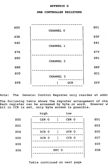
APPENDIX G DMA Controller Registers
APPENDIX H SCSI Controller Registers
APPENDIX I Control Register
APPENDIX
J
CC74 Program Example
APPENDIX K Data Sheet 68450 DMAC
APPENDIX L Data Sheet 5385/6 SCSI 'Controller
A-I
B-1
C-1
D-1
E-1
F-1
G-I
H-!
1-1
J-1
K.,.!
L-1
•
•
•
•
•
•
•
•
•
.. '1
•
•
•
..
•
~
I
..
~CHAPTER 1
GENERAL INFORMATION
1.1 Introduction
The
CC74
module interfaces the VMEbus and Small Computer System
Interface (SCSI) with
each
other.
Th~smanual
gives
a
full
description of
the
hardware
and software for users and system
programmers. For specific details about
the
VMEbus,
SCSI
bus,
SCSI
protocol
Controller or DMA
controller,
the
following
documents may also be consulted.
VMEbus specification manual
-
SCSI specification manual (ANSC X3T9.2)
-
SCSI protocol controller user's guide (see appendix L)
-
SCSI protocol controller data sheet (see appendix L)
- DMA controller data sheet (see appendix K)
1.2 Features
The CC74 VME-SCSI interface module features the
high-performance
68450
DMA
Controller and the NCR 5386 SCSI Protocol Controller .
The SCSI Protocol Controller conforms to the
ANSC
X3T9.2
Small
Computer System Interface standard.
SCSI features:
- Asynchronous data transfer up to 1.5 MByte/s
- Supports both Initiator and Target role
- Parity generation with optional checking
-
Supports Arbitration and Reselection
- Controls all bus signals, including Reset
....; DMA or programmed I/O transfers
- Block transfers up to 16 MByte
VME features:
- DMA Controller supports I/O to memory, memory to I/O
and memory to memory transfers
- Optimal bus width utilization for mixed byte and word
transfers
-
Programmable Interrupt and Bus Request levels
-
Programmable Interrupt vectors
-
Interrupts VMEbus when SCSI bus requires service
-
23 bit addresses, 16 data lines and 6 AM code lines
- Highly reliable data transfer by error detect, error
interrupt vector and exception features
All
SCSI
connector
connector.
I/O
and
signals are
also on
a
1.3 General Description
available on the I/O pins of the P2
SCSI-compatible
50-pin flat cable
The Small Computer System Interface (SCSI) is a de facto industry
standard and
is used to interconnect small computers with each
other and with
intelligent peripherals such as
hard disks,
flexible disks,
magnetic tape devices etc. The standard defines
the bus protocol, the bus drivers, cables and connectors and
the
command set. The CC74 module is a full implementation of the SCSI
standard and may act as an Initiator or Target on the SCSI bus.
The 8-bit data transfers between the SCSI bus and the VMEbus
can
be handled by any DTB master or by the local DMA controller. The
DMA controller can also be used for memory to memory transfers on
the VMEbus and may be used by a RAM disk routine. The CC74 has
a
four-level Bus Requester and a seven-level Interrupter, which are
both software programmable. The normal and error interrupt vector
can also be dynamically installed.
Manual CC74 Ver 1.3
1-2
January 1986
c
c
•
1
,~
I
•
CHAPTER 2
SPECIFICATION
2.1 VHEbus Options
Data transfer options:
- DTB MASTER
A24,A16; 016,08
- DTB SLAVE
A24,A16; D16,D8
Requester options:
- Anyone of R(O) R(l) R(2) R(3)
(DYN)
-
RWD
~
Interrupter options:
•
1
•
•
-~
l
•
- Anyone of I(l) 1(2) 1(3) 1(4) 1(5) 1(6) 1(7)
(DYN)
- Normal interrupt vector
(DYN)
-
Error interrupt vector
(DYN)
Environmental conditions:
- operating temperature
- max operating humidity
Power supply requirements:
0-70 degrees C
90
%
-
3.0 A max (2.7 A typ) at 5 VDC
Physical configuration options:
- NEXP
2.2 SCSI Bus Options
The following options are implemented on the CC74 module.
-
Supports ANSC X3T9.2 SCSI standard
-
Supports Arbitration and Reselection
-
Single-ended drivers and receivers
-
Non-shielded cable option
-
Performs both Initiator and Target role
-
Parity generation with optional checking
- Controls all SCSI bus signals
c
,.
i III
c
•
•
•
•
•
•
•
•
CHAPTER 3
INSTALLATION INSTRUCTIONS
3.1 Introduction
This
chapter gives
all necessary preparation and installation
instructions for the CC74 VME-SCSI interface module.
The
module
can be· used
in VMEbus
systems
and configuration options are
selected by jumpers and switches. All settings are illustrated as
seen from
the component
side with both VMEbus
connectors
downwards.
Jumper blocks are drawn using
' 0 'for each pin except
pin
1
which is identified as
'*'
3.2 Address Selection
Jumper blocks JBl and JB2
are
used
for
the
address modifier
selection.
JBl
when installed will make the CC74 module respond
to supervisory access only.
*
JB1:
o
*
JB1:
o
supervisory or
non-privileged access
supervisory-only access
JB2 is used to select standard or short address decoding.
JB2:
* - - - 0 0 - - - 0standard addressing
JB2:
*
0 - - - 0o
short addressing
Switches Sl-S4 are hexadecimal switches used to select
the base
address of the module. Sl selects the most significant nibble, so
the
address
lines
A23-A20
are
selected by Sl, A19-A16 by S2,
A15-A12 by S3 and All-A9 are selected by S4. Note that S4 selects
3 address lines and thus has only 8 significant positions
(only
even numbers). Also note that Sl and S2 are not significant when
JB2 is installed for short addressing.
3.3 DMA Clock Selection
Jumper JB3 is used to select the OMA clock input. When an
8
MHz
OMAC
is used, a derivative of the system clock can be used. When
a 10 MHz OMAC is used, the SCSI Controller clock may be used
and
for
other clock rates the
optional oscillator U18
must be
installed. Jumper JB3 must be set according to the installed OMAC
type.
* - - - 0
JB3:
0 0OMA clock-rate defined by U18
0 0 * 0
JB3:
0 - - - 08 MHz OMA clock rate
0 0 * 0
JB3:
0 010 MHz DMA clock rate
0 - - - 0
3.4 SCSI ID Address Selection
Any Initiator or Target module on the SCSI bus must have a unique
IO-bit. Eight
10
bits are defined and can be selected with jumper
JB4. Only one jumper must be placed at JB4.
ID bit
7
6
S
4
3
2
1
o
o
o
o
o
o
o
o
*
JB4:
I
o
o
o
o
o
o
o
o
10
bit 2
selected
3.5 External DMA Devices
The jumpers involved with external DMA devices are JBS,
JB6
and
JB7.
The
programmable
control
lines can be used for input or
output. JBS is used to select the direction of the
PCL2
control
line.
Manual CC74 Ver 1.3
3-2
January 1986
•
i
•
c
It
II
•
•
•
•
-~
•
•
III
j
!
III
III
III
•
II
.. ~
lilt
-~
lilt
--~
*
o
JB5:
I
PCL2 configured as input
o
o
*---0
JB5:
PCL2 configured as output
0---0
JB6 selects the direction of the PCL3 control line.
* 0
JB6:
I
PCL3 configured as input
0 0
*---0
JB6:
PCL3 configured as output
0 - - - 0
JB7 is used to select the direction of the DONE signal.
* 0
JB7:
I
DONE configured as input
0 0
* - - - 0
JB7:
DONE configured as output
0 - - - 0
Jumpers JB5, JB6 and JB7 can be removed when not using the option
for
external DMA devices. When using this option i t is necessary
that there shall be no conflicts between the programmed direction
and the installed jumper settings of the control lines.
3.6 SCSI Bus Termination
The SCSI bus consists of a 50-pole flat cable which may be 'daisy
chained' to a maximum of eight Initiator and/or Target
devices.
Both
devices
at the
ends
of
the cable should have installed
terminating networks and all other devices must
not
have
these
networks. The CC74 module has the two relevant resistor networks,
RNI
and
RN2,
installed in sockets, and these networks must be
removed when the module is not at the end of the daisy chain.
In some SCSI bus systems, the power of the
terminating
networks
is supplied
by
a 'Terminating Power Supply' via pole 26 of the
SCSI cable. This pin is referred to as 'TRMPWR'.
Jumper
JB8
is
used
to
select the
power
source
for
the on-board resistor
networks.
~
~
*
I
~
JB8:
0VMEbus power connected to on-board
resistor networks
0 II
~
*
JB8:
0SCSI bus 'TRMPWR' connected to on-board
~
I
resistor networks
0
~
~
~
I
..
~
•
~
~
C
~
I.
~
~
C
~
I.
C
C
C
C
Manual CC74 Ver 1.3
3-4
January 1986
•
•
•
•
•
•
-~
•
•
~
I
CHAPTER 4
THEORY OF OPERATION
4.1 Introduction
This chapter gives a global explanation of the functional
blocks
as
shown
in appendix
A.
The
schematic diagrams are given in
appendix B. The main functions of the CC74 module
are 'performed
by
the
68450
DMAC
and
the NCR 5386 SCSI Protocol Controller.
These
two
parts
are
fully
described in the
manufacturers
documentation included in appendix K and L.
4.2 DMA Controller
The 68450 DMAC has three modes of operation.
In
the MPU mode, the DMAC is selected by an external bus master,
through a chip select or interrupt acknowledge. The bus master is
writing or reading the contents of the DMAC internal registers.
In the DMA mode, the DMAC
is the
current bus
master
and
is
transferring data or preparing for the data transfer.
In
the
IDLE
mode, the DMAC is in a state other than MPU or DMA
mode. A Read/Write access or transfer request will
change
the
mode into MPU or DMA respectively.
4.2.1 MPU Mode
In MPU
mode,
an
access
is made
to one of the DMAC internal
registers. The registers can be accessed by byte or word.
There
are
64
bytes
defined per
channel
and
each
channel
has 17
registers. There are four channels available, so the
DMAC
takes
256
bytes in the memory map. The address lines Al through A7 and
the data strobes determine which register will be selected.
When
an
interrupt
acknowledge
cycle
is performed
the
DMA
controller puts
the
contents of the normal or error interrupt
vector register of the highest channel requesting an interrupt on
the data bus. The
DMAC
uses
a
multiplexed
address/data bus,
demultiplexing
is done
by U7-UIO with the control signals DDIR
(Data DIRection), DBEN (Data Bus ENable) and UAS
(Upper
Address
Strobe).
4.2.2 DMA Mode
When
in DMA
mode,
the
DMAC
is the current VMEbus master and
activates the OWN line; this will
enable
the buffers
of the
VMEbus
interface.
Transfer modes
used
for DMA are defined as
follows:
Dual addressing with auto request:
- transfer byte or word from memory to holding register.
- transfer byte or word from holding register to memory.
Single addressing with request acknowledge handshake:
- transfer byte from SCSI PC to memory (using 00-07).
transfer byte from SCSI PC to memory (using 08-0lS).
transfer byte from memory to SCSI PC (using 00-07).
transfer byte from memory to SCSI PC (using 08-015).
Timing and control signals are generated by UlS, U16 and U29.
4.3 VMEbus Interface
The main part of the interface to the VMEbus
is given
in the
schematic
diagram
(Appendix B,
sheet I). The address and data
lines are shown with their respective buffers to the VMEbus.
The
control
signals for
these buffers are; GVME to enable the data
buffer on the VMEbus, FROMVME to control the
data direction of
the data buffers,
and OWNL wich is used to enable the address
buffers. These control signals are generated by U29
(sheet 7).
The
multiplexing of the address and data lines is performed by
the DMAC using the signals UAS (Upper Address Strobe), DDIR (Data
DIRection) and DBEN (Data Bus ENable). The control lines on the
VMEbus are buffered by U14, U26 and U27 (sheet 4). The generation
of DTACK
(when
in MPU mode) is performed by U1S (sheet 7) and
buffered by U24 and U30. A shift register US2
is used
for the
DTACK timing.
4.4 Address Decoding
The
address decoder
is
given in the schematic diagram of sheet 2
and uses the address lines A9-A23 and AM code lines AMO-AMS.
The
LIACK
signal
is used to inhibit address decoding when an lACK
cycle is performed. Jumper JB2 is used
to enable standard or
short
addressing,
and
JBl
to select
supervisory-only or
non-privileged access. The remaining modifier codes
select data
I/O access.
4.5 DTB Requester
The
onboard DTB
requester consists of two parts, the requester
logic U20 and the chaining logic U2l. The bus request logic, when
activated by LDBR (Local DMA Bus Request) will assert one of the
BRx
outputs depending
on the installed request level (REQLVO,
REQLV1). Now i t will wait for a Bus Grant (BGT) from the chaining
logic. The chaining logic checks the incoming BGxIN signals
from
the VMEbus and determines if the incoming signals must be chained
toBGxOUT
or should be
used
locally.
Latch U19 is used to
guarantee a valid BGxIN signal for the chaining logic. The
level
of bus request is software-selectable and is discussed in chapter
5.5.
Manual CC74 Ver 1.3
4-2
January 1986
~
•
•
I
•
•
•
•
,
•
1
I
•
•
-~
-~
•
•
-~4.6 Interrupter
The
Interrupter U22
(sheet 3) uses the latched VMEbus signals.
This circuit asserts one of the seven VMEbus
interrupt signals
(IRQI-IRQ7) when a local OMA interrupt (LIRQOMA) is received. The
interrupt
level
is determined by IRQLVO-IRQLV2 and is software
selectable (see chapter 5.4). When an interrupt has been asserted
the interrupter waits for an Interrupt acknowledge cycle on
the
VMEbus. Then the interrupt level will be checked and when a match
is found IACKSEL will be asserted, otherwise IACKOUT is asserted.
The
OMA
controller will generate the proper interrupt vector,
when necessary. When an interrupt acknowledge cycle for the OMAC
is performed,
the
interrupter releases the VMEbus IRQ line and
will only respond to another IRQOMA, after negation of
LIRQOMA
for at least two clock cycles (125 ns).
4.7 External OMA Devices
The
68450
is a four channel OMAC and only two channels are used
by the SCSI interface.
The
control
lines of the
two
unused
channels
are connected to the
P2 connector. The direction of
these signals can be selected by jumpers. The
two
channels
may
therefore be
used by other devices on other modules via control
lines on the P2 connector. Care should be taken here
to prevent
conflicts with the VMEbus
specification;
however, relatively
simple I/O modules may take advantage of these OMA channels.
4.8 SCSI Interface
The SCSI protocol controller used is the NCR 5385 (or NCR
5386).
Sheet
5
of the schematic diagrams shows the complete interface.
SCSI bus buffering is performed by U42 through U47. Units U40 and
U41 are used for driving one of the eight data lines on the
SCSI
bus
during
arbitration.
JB4
selects which data line will be
driven during arbitration, the so called 10 address. U36
encodes
the
JB4
setting into three 10 signals 100, 101 and 102, used by
the SCSI PC. U39 (sheet 6)- is a 10 MHz clock oscillator for
the
SCSI
PC
clock. Connector P3 is a flat cable connector which has
the proper SCSI bus pin definitions. Connector P2 is the standard
VMEbus
I/O
connector which has
also all SCSI
bus
signals
connected.
Anoptional module CC85 is available to interface a
50-pin SCSI bus flat cable to the P2 connector.
•
•
•
•
•
-~
•
CHAPTER 5
PROGRAMMING CONSIDERATIONS
5.1 Introduction
This
section contains
all necessary
information
for
system
programmers
to take
full advantage of .the features of the CC74
module. Additional information may be
found
in the
respective
data
sheets of the SCSI protocol controller (NCR 5385/6) and the
DMA controller (68450). For system programmers who want to write
their
own
CC74
driver software,
a
full
understanding
and
experience
is required.
The
source
code
of
a
sample
driver
routine for this module is found in Appendix J.
5.2 Memory Map
The
memory
map
is given
in Appendix F. The module takes $200
(=512) byte locations, starting at the selected base address. The
first 256 locations are used
for
the
DMA
controller and
the
second
block is partially used by the SCSI controller (16 bytes)
and the local control register (1 byte). Both the SCSI controller
and the control register are 8 bits wide and are accessed at odd
memory
locations.
Both are duplicated an arbitrary number of
times in the memory map. The recommended
address
locations
for
use by system programmers are given below.
BDMAC
CNTREG
B SCSI
equ
equ
equ
CC74 BASE+O
CC74-BASE+$100
CC74-BASE+$120
base address for DMAC
address of control reg.
base address for SCSI PC
CC74_BASE depends on the address select switches Sl-S4. Note that
the
byte
wide
registers respond
at odd
addresses only. The
registers within the DMAC and SC$I PC can be
accessed by using
B DMAC
and
B SCSI as the respective register base addresses and
declaring each-register as an offset from
these
addresses
(see
Appendices G and H)
5.3 Reset
The
SYSRES* signal from the VMEbus will reset the DMAC, SCSI PC,
DTB Requester and the
local
Control
Register.
When
the
DMAC
recognizes
Reset,
i t relinquishes
the bus, clears the GCR and
resets the DCR, OCR, SCR, CCR, CSR, CPR and CER of all
channels.
The
interrupt vector
registers
are
set to $OF (uninitialized
interrupt vector number).
When
SYSRES*
is active,
the
SCSI
Protocol
Controller
is forced
into a reset state. All current
operations
are
terminated
and
internal
storage
elements
(registers,
counters
etc.)
are cleared. A 'chip reset command'
loaded into the SCSI
PC
performs
the same
operation as
the
hardware reset. The DTB Requester falls into the idle state after
reset,
which
means
that all output signals are negated (no bus
requests active). The local
control
register will
be
cleared
after reset and all output lines will be low. This disables the
interrupt request level, the bus request level will be 0 and
the
SCSI
reset signal will NOT be activated. The SeSI reset signal
when activated (by a write instruction to the Control
register)
will
reset the SCSI PC, which will then release all bus signals
within a 'bus clear delay'. The Interrupt handler attached to the
CC74 module can be informed about the SCSI Reset
condition with
an
interrupt request. The PCLl line of the DMAC is used for this
purpose.
5.4 Interrupts
All interrupts from the CC74 module are generated by the DMAC.
These
interrupts can be
caused by several conditions such as
channel operation complete, PCL transition or Bus
error.
Each
channel
may generate its own normal interrupt vector or an error
interrupt vector. An error interrupt vector is generated when
a
DMA
transfer is terminated by a bus error response or when an
address error occurs. In the case of an error, the present values
of the Memory Address, Device Address and Base Address registers,
the Memory Transfer and
Base
Transfer counters,
and Control,
Status and Error registers will be
available. The interrupt
signal of the SCSI PC is connected to the PCLO input of the DMAC
and
may
also cause
an
interrupt on the VMEbus. The interrupt
signal from the DMAC is sent to the Interrupter which will assert
the proper interrupt request
line.
The
interrupt level
is
selected by the Control
Register outputs
IRQLVO, IRQLVI and
IRQLV2 (3 binary encoded level outputs).
IRQLV2
IRQLVI
IRQLVO
INTERRUPT LEVEL
---
---0
0
0
(disabled)
0
0
1
1
0
1
0
2
0
1
1
3
1
0
0
4
1
0
1
5
1
1
0
6
1
1
1
7
c
c
Bit 3 of the Control Register may be used to disable the DMAC IRQ
C
line. This bit is used by the interrupt routine as follows.
-disable IRQ line (set bit 3).
-process the normal interrupt routine.
~
-disable IRQ line (clear bit 3).
~
This procedure is necessary to guarantee the proper working of
the Interrupter.
~~
c
Manual CC74 Ver 1.3
5-2
January 1986
•
•
•
•
5.5 Bus Request
When the DMA controller needs control of the bus i t will generate
a
DMA
Bus
Request to the DTB requester. The level on which the
DTB requester will generate a Bus Request on the VMEbus
depends
on
the
REQLVO, REQLVI outputs of the control register (2 binary
encoded level outputs).
REQLVI
REQLVO
o
o
1
1
o
1
o
1
BUS REQUEST LEVEL
o
1
2
3
•
The DMAC controls VMEbus utilization and request interval timing.
The Burst Transfer Mode, Cycle Steal Mode with or without hold,
.~
Burst time and Bandwidth Ratio are also under software control .
..
-~
..
..
..
..
..
-~
..
5.6 Control Register
The
Control
Register
performs several functions. It is used to
select the levels for the DTB Requester and the
Interrupter and
to enable/disable the
DMA
IRQ
line.
It is also
used
for
monitoring the SCSI
Reset
line
(LRSTI)
and may
be
used
to
activate the SCSI Reset line (LRSTO). Note that when LRSTI is '1'
and
LRSTO
was
written as '0', means that another device on the
SCSI bus is asserting the reset line. The following
table shows
the bit assignments of the Control Register.
BIT
READ
WRITE
FUNCTION
--
---0
IRQLVO
IRQLVO
1
IRQLVI
IRQLVl
Interrupt Request Level
2
IRQLV2
IRQLV2
3
ENIRQ
ENIRQ
Enable DMA IRQ
4
REQLVO
REQLVO
DTB Request Level
5
REQLVI
REQLVI
6
Spare
Spare
Not used
7
LRSTI
LRSTO
SCSI Reset
5.7 AM Code Generation
When
the DMA
Controller
is in the DMA mode, i t will generate
Function Codes on its FCO-FC2 lines.
These
lines
are
software
programmable for source, destination and base address access (see
chapter
5.8.1). A translation of these lines
is
made to generate
the
six
Address Modifier code lines on the VMEbus. The
following
table shows the translation and function of the respective lines.
FC2 FC1 FCO
AM5 AM4 AM3 AM2 AMI AMO
FUNCTION
--- ---
---0
0
0
1
0
1
0
0
1
short n.p. I/O
0
0
1
1
1
1
0
0
1
stand n.p. data
0
1
0
1
1
1
0
1
0
stand n.p. prog
0
1
1
1
1
1
0
1
0
stand n.p. prog
1
0
0
1
0
1
-1
0
1
short priv I/O
1
0
1
1
1
1
1
0
1
stand priv data
1
1
0
1
1
1
1
1
0
stand priv prog
1
1
1
1
1
1
1
1
0
stand priv prog
5.8 Programming the CC74 Module
Programming
the CC74
module
can be
divided into two main
sections: programming the DMAC, and programming the SCSI Protocol
Controller. It is also necessary to program the desired interrupt
and bus request
level
as discussed
in chapter 5.4 and
5.5
respectively.
In chapter 5.8.1 the programming of the DMAC is
discussed. Chapter 5.8.2 discusses the programming of the SCSI
PC. A programming example is given in Appendix J.
5.8.1 Programming The DMA Controller
The
68450 DMAC
has internal control registers and performs the
required operation by means of control
words
written in these
registers by the MPU.
A normal
programming
sequence can be
divided into three phases.
~
The Initiation phase: MPU sets up control
registers,
transfer
~address and transfer counts.
The
Transfer Phase:
DMAC receives requests and transfers data.
The DMAC
writes the transfer status into the error
register and
the
internal status register after the
completion of the transfer.
The Termination Phase: The MPU checks the post-transfer status.
The internal registers are shown in Appendix
G
and
a
short
description is given below.
The Device Control Register designates an external I/O device. It
will
set the external request generation method, the
device type,
the device port size,
and
PCL
line
operation.
c
c
c
The Operation Control Register designates the transfer operation.
C
....
It designates
the data transfer direction, the operand
size,
the chain operation types,
and
the
request
generation method.
~Ia.
•
The
Sequence Control Register designates the increment/decrement
sequence of both memory
and
device
(source
and
destination) addresses.
The Channel Control Register designates the channel operation. It
~
designates
operation start,
the
continuous-operation
~
setting, HALT, abort, and the interrupt enable/disable.
•
The Channel Status Register contains the channel status. It shows
channel operation completion, block transfer completion,
normal
termination, the error status, the channel active
state, and PCL signal line information.
I
The Channel
Error Register indicates what
error types have
occurred.
I
The
Channel
Priority Register determines
the priority of the
channel.
•
•
•
•
•
•
The Memory Transfer Counter is a l6-bit register to hold transfer
counts. The block size (transfer count) is written when
one
data block is transferred. When multiple blocks are
transferred in Continuous Mode
or Chaining Modes,
the
next block size is automatically loaded in the MTC after
completion of the previous block transfer.
The Base Transfer Counter is used in Continuous Mode
and Array
Chaining Mode. In Continuous Mode the first block size is
stored in the MTC and the second block size in the BTC.
The content of the BTC
is copied into the MTC
after
completion of the
first block transfer. When more than
two blocks are transferred in this mode, the BTC and BAR
(described later)
are rewritten and the CNT bit in the
CSR is set again during
the
second
(or third)
block
transfer.
In Array Chaining Mode,
the BTC holds the
number of blocks being transferred.
The Memory Address Register contains the memory
address being
output
for each transfer cycle. In block transfer, the
beginning address of the block is written in the MAR
as
an
initial value.
And
the content of the MAR varies
according to the contents of the OCR and the SIZE bits in
the SCR after one operand transfer.
In Continuous Mode
and
Chain Modes,
the MAR is rewritten according to the
BAR or the array information in memory
when
a
block
transfer completes.
The
Device Address Register is used to address an I/O device (or
to address memory, in memory-to-memory transfer). The DAR
is used only in Dual Addressing Mode,
and changes
its
content according to the SCR and according to the SIZE
bits in the OCR.
The Base Address Register is used in Continuous Mode
and
Chain
Modes.
In Continuous Mode,
the
start address of the
second block is written in the BAR. This BAR is used in
the same way
as
address where
the
contained.
the BTC. In Chain Modes, i t keeps the
information of the next block is
The Memory Function Code, Device Function Code, and Base Function
Code
Registers
are used together with the MAR, DAR, and
BAR respectively. The MFC, DFC, and BFC are used with the
same purpose as the FC outputs from the MPU.
This makes
i t possible to transfer data between supervisor program
area and user data area, for example.
A translation is
made to generate VMEbus AM codes from the Function Codes,
this is discussed in section 5.7.
The
Normal
and Error Interrupt Vectors keep the vector numbers
outputted in the vector number
fetch cycle
(Interrupt
Acknowledge
Cycle).
When no error has occurred (ERR bit
of CSR is not set), the DMAC outputs the NIV
contents.
When
an error has occured (ERR=l), the DMAC outputs the
EIV contents.
The General Control Register is common to all four
channels
and
determines
the DMAC's bus use ratio and sample interval
in limited Rate Auto-Request Mode.
In Maximum
Rate
Auto-Request
Mode, the DMAC takes the bus mastership and
transfers all operands until they are exhausted. In this
mode, when the higher priority channels request transfer,
the channel with the Maxixmum Rate Auto-Request stops its
transfer temporarily and the higher priority channel is
serviced. The Maximum Rate channel resumes
its transfer
after the priority channel has been serviced.
After the DMAC is properly initialized, a transfer is started by
setting the STR bit in the Channel
Control Register.
When
the
DMAC
completes a transfer operation, the COC (Channel Operation
Complete) bit in the CSR is set. If an error occurs during the
transfer,
the ERR bit is also set. If the INT (Interrupt Enable)
bit has been set, the DMAC will issue an interrupt request when
the COC
bit is set. If Interrupts are disabled, the MPU should
poll the COC bit. The transfer termination routine should check
for errors.
Error routines should be programmed case by case
according to their applications. For bus error and address error,
the CER (Channel Error Register) can show which address register
caused the error and the address where the error occurred is kept
in the address register. The CER also shows which of the transfer
counters between the MTC and BTC caused the error.
5.8.2 Programming The SCSI Protocol Controller
The
SCSI
Protocol
Controller has
a
set of 13 internal 8 bit
registers, which are used to read or write data,
status and
control
information. A summary of the SCSI registers is given in
appendix H. Note that some registers are read only.
A normal
programming sequence where the CC74 module act as an Initiator on
the SCSI bus is as follows.
•
•
•
•
•
•
•
•
~
i
,
•
•
•
•
1. Arbitration phase; Initiator arbitrates for the bus.
2. Selection phase; Initiator selects a Target.
3. Prepare SCSI chip and DMAC for data transfer.
4. Message-In phase (optional).
5. Command phase; give command to Target.
6. Data phase; transfer data (optional).
7. Status phase; get status from Target.
8. Receive command complete message.
9. Wait for disconnection.
10. Check for errors.
When
the
CC74 module acts as a Target, the programming sequence
can be as given below.
1. Wait for selection.
2. Initiate a Message-In phase (optional).
3. Command phase; get command from Initiator.
4. perform command.
5. Data phase; transfer data (optional).
6. Status phase; send status to Initiator.
7. Message phase; send message to Initiator.
8. Disconnect initiator.
9. Idle mode.
Before any operations
are performed,
an
Internal
Diagnostic
Command
should be
given and
status information checked for
succesful
completion.
After power-on
Reset,
the
Internal
Diagnostic Command is automatically executed.
i
II
c
c
"
I
.i;
APPENDIX A
•
BLOCK DIAGRAM
,,~
•
--~
•
.-•
C<
•
"
•
SCSI CONNECTOR
I
VMEbus P2-*-i
I
III
\ '
S(SI BUS1
"
,III
,.
684513
III
~ OMAC
..
"'1:
.-.~
ADDRESS (ONTROL SCSI DE[ODER
I
REGISTER iNTERFACE
I
I I
I
I
1I
I
BUS (ONTROl!
I
I
L
\ DATA &
LO[Al DATA BUS
F
'Ooms
I
I
BUS BUFFERS
AC:JRESS BUS
I
I
I
ADDRESS BUS DATA BUS
I
CONTROL BUS DTB REQUESTERBUFFER BUFFER BUFFER INTERRUPTER
I
•
I
i
"I
VMEbus
..
•
- -.
..
-'l
•
I
III
,.
!
APPENDIX B
SCHEMATIC DIAGRAM
•
Sheet 1
DMAC-VMEbus interface
Sheet 2
Chip select logic
•
Sheet 3
Interrupter / Bus requester
Sheet 4
VMEbus interface
•
Sheet 5
SCSI interface
Sheet 6
SCSI-DMA transfer
&
control logic
-$1
Sheet 7
Local data path
•
Sheet 8
68450 DMAC / NCR 5386
Sheet
9
SCSIbus connector / power supply
Sheet 10
Decoupling
Sheet 11
VMEbus connector PI
Sheet 12
VMEbus connector P2
-~
-'l
l1li
III
..
-,.
..
Appendix CC74
B-1
January 1986
!
•
~
III
F
o
,.
14lS313III
"I III
"
III·SV .5v
P.=t~
U10
4 RN7 I 9 RIll. I - II (I A23/0 I S B 18 10 t>
1.221014 )4 3
35 17
1.21/013
36 4
A28/012
"
14AI9/011 37
38
"
7A18/018 39
"
13A 17/09
A 16/08 4il
"
B 24
•
UAS 61 5 1 U)5 674LS373
1
•
);~
•
U 1
11.lSIII.P.=t~
- II (I
U9
41 18 10
A15/07 I>
AII./06 42 3
AIlIOS 43 17
AI2/01. 44 4
AII/03 45 14
AIB/02 46 7
A9/01 41 13
ABIOB 48
"
B"
,,;;
•
4~4
U3574LS81.
i
OliN 68 1 1 2 OIiNHU35
..
74LS81. 1I.LS645"1
III
519
G3
U7
·SV~
3ENI~
3EN2-,
"-
A23/DIS 9rVI <l t>"-
A22/0 II. 8,~
"-
A21/o1) 7"-
AZB/D12 6III
"-
AI9/011 5"-
A18/01B 4"-
AI7109 3.'~
"-
A16/08 2III 6 DB EN
63
74LS64S
>i
II
"~
·5V 19
U8
113 1 RN4 6 I
3ENI 00111 64 L 3["2
- - ,
"-
AIS/07 9r: VI <lt>
"-
A 14/06 8"-
A 13/05 7..
"-
~ 12104 6A 11103 5
A10/02 t.
~ II
i
cco "81
II II
~
1
"-
A9/01 3I A8/0B 2
I
OMA( 681.50·5v
a RNI. 1
I
HIBYT[
62~BYTE
I
REV- DATE1 ·13 1-135-8t.
..
1 ·2 7-313-85.~ 1 ·3 11-28-85
•
'~~
,~ B 74f21.1.P.t'
19 EN2U2
V 19 2 t> IV 18
2 17 t> 2'1 )
16 I. 16
I> IV
.5 IS S
IS 6 t> 2'1 II.
I> IV
6 13 7
12 8 I> 2'1 12
I> IV
9 II
I> 2'1 9
74f2H
~'
ENZU3
19 2 18
V I> IV
2 11 t>
2'1 3 16 I.
I> IV 16
5 15
I> 2'1 5
15 6 t> IV II.
6 13 t>
2'1 1
12 8
I> IV 12
9 11 t>
2'1 9
OIlNl
74AlS645A-I
GVHE~ li3
US
FROMVME--l:::
3ENI3EN2
r- 11 '---, r- 11
:J.
LOIS 9CV1 t> <l"I.
2V 12 LOll. "- 8 ZV 1213 Lon "- 1 13
11. LO 12 "- 6 II. IS LOll " 5 IS 16 LO 1 B "- I. 16
17 L09 "- 3 17
18 L08 "- 2 18
"-74ALS6t.SA-1 19 U6 IlVHE 63 FROMVI1E 1 3ENI
L 3EN2
r - 11 '---, r- II
h-
LOl 9rV1 <li
I>
2V 12 L06 "- B 2V 12 13 LOS "- 7 13
14 L04 6 14 15 L03 " S IS 16 L02 "- I. 16 17 LOI "- 3 17
18 LOB "- 2 18
LOB-LOIS
COMPANY
HP
T[0
[ON ROL 8 V
EINDHOVEN-HOLLAND
T I HE
OMA[-VMEbus
INTERFACE
"OOULE SHEET
AI-H3
"
"-'\. "- I'-'\.I
"-PIm
Am
A23 22 21 28 19 gf-A
Cl8 A
~A
~ A18 A17 A16 (21
'Ctr
'-=-=-PI'cIT AI5
2
ill
ill
At4 3rn
ill
ill
m
TIe
=
PI """"(8 '(7r-c6
res
f(t f(3 1--(2r-t1
PI~
"7 A6 AS ,At-AT"
Az
A1
"-"-'-A13 A12 All A18 A09 ABa 015 014 013 012 011 018 oe9 DBa 087 086 085oel
oe3
D02 OBI OBe OF~1 ~
o
~-I "I
I COMP
61
A16 2 9
I>
A 18 ---~
.,9
8
A20 _ _ _ _ -1.' P
A21 13
I
A17 4 }
U 11
A22 IS
,~v
A23 17 7~19
SITifiGli~
s
~[~ ~;
B} IP.Q
-S2
F 3 4 7 9 7 91 8 12 Q AH4
0( 2
6 14
F 3 4 16
S 1
4 2 18r
s
16
6
1
74L5688 COMP
PAL 2
e
G
}'
J13
P
fU16
0\7IIT
--,-7
r-nn
_2_LURllE _5_
ITKl! _6_
o
ii8'fNm_
_7_a_
X/Y
fPLA
8
V 19 HLDADA V 18
rvsm
V 11 IJ1VmV 16
m
V 15 DIA(k V 14
V,13
Vet='2
V II
V 9
0} IP.Q 19
is[ijSf!
~7 825153
IQ_t'~V
~
N -
mf
,J"'~I
PI
~ ---~ ~---~
rnre---~
ABS
1TIil---'
IACk5EL ---~I-- 10 7
~,RN5
'----.. ---,--
1 -~-~r----,--_,_--4-=C=s
~
..---.
.-.
.---.
w-w
~ ~.,-.
r - .
REV.
I·
a
I ·2
1·3
.--.
DAlE COMPANY
(OHP(ONTROL S·V·
8-81-84
EINDHOVEN-HOLLAND
7-30-85
11 H(
11-28-85
(HIP SELE(T LOGI(
MODULE
I
SHU 1( (74
02
.---w
.--.
~ ~ ~---9
A
8
D
Of
12
~
L.Jt.i
II
-~II
.~___ ...
~L
~. . . . . .
"_.11
____ •
~ ~...
.AiI L_.Ai • M • • . . i i.:Ii ... __ .
..II!A
BI
o
UK 16
mlrn
LI ROOHA
ITS!
lA3 lA2 LAI IROlV0 IROLVI IROlV2
BliIlIH* BGI IN. Bfi2IN. BCi3IN •
m
I A(K
'"*
ifiR1i fiBii
IiBffii
[TAn
I
!i 6I
7I
8I
9.5V 5
.
H---
s
U 17
t--=-
J
74lS641-1 I...---+-i
3M>(
I 19U
24-IAuoua
PALS
l4-
10 6fIr
G3- 13 I 12 I R 3 E N I .
-1 LAS 3£N2
61
U 2 2
U35 74F74 c.., r- mTIiII fH2 14LS94
U23
''c
02 <Ii-L
v~
IROLV9+
9) 11 0~
mrn
12 1> 10 8Tie
+ ']
\::.la I ROL V I3
{j -:; I 13 13 7m
-J-
V!'+'" IROLV2 --"- 2 2 12 14 6Ifii
-4-
102vH~
4 [J0X 3 II IS Sm
~
10'2vHoe
.
i:"ilfO'Di1A*
& 4 1 B 16 4~
-4-
I1O'2V~
IACKSfL~
S 9 1 7 3 m-+-
10: 217 14 6 7 1 8 2 m~
9 V~ 13 7=
- : . - 8 Vr"12 74LSI38 741S641-1
II EH2 HNI
IROU IR02. IR03, IROU IROS. IROU IR07.
PA116R4
~
(LKI6 I GIU20
PAL6Pr~
G3U25
3[N22
V~
18_~2
<lL',....,2 PI.r--t- ']
I 8 lJ"II1 I I> I 0 I Irffr
~ 10.217 17 '\ LaR 17 3
'itt
rnn S i D . 217 16 LBR2 16 4TIt
LOeGACK 6 I 10,217 15 LBR3 IS S'itS
REOLV0 7 10.217 14 '\ 14 6
7f
REOLVI 8 10.217 13
L
Elf"
~'-=-r-t-
lO.2V~m
12 ~m
--+-~B
v 12 G PUP 11,...!.
PAL 16R6
:::J
I PAL 7LRESET --l---~""--' CLKI6 GI
U21
I I EN2BRB.
SR ..
BR2. BR3.
BBSY,
,..._---
m!
2 V~ClKI6
-1...L~C1
~ ~
3 ' ] ' 0 217 18 PIm
,.-L.
ENU 19
L-e-R3 '"~
10: 217:~
~
PI -L r 6 I
:~,;:
IS*
;$:
--+
10t>
v~~
~
10: 2v-f}Jli::
~
4 21 9 10.217...,.JA
S 20 8 12.!!.!
6 19Vn
!TIIJ----+
*1-
1I A [k I N 11.r;-b...J.!. • 5 VI
P A1I6 R6I
mT---~-
~I-
LOBRl....:..JU3S
~:
---~~
~I--
tD'BUrK 14lSIl4 REV. DAlE COMPANY_______ .lL
f-.l!!-
~ [11'6'jj"Hl (0I 00 1 • iii 1 -135 - 8 5 E I
AM29921 2
~--t 1.2 7-313-85
1 2 ""'--7"",-' 11 T l£
&V~p:....l.L
1.3 11-27-85 INENIRO 13 U39 BU
74538
MOOUL[
BGIlOUTI BGIOUa 8G20UTI 8G30UTl
HP(ONTROL
B·V-NDHOVEN- HOLLANDTERRUPTER S REOUESTER
SHEET --,-_ _ · = : I I . -3--- -1- ---4--- ---- -
e
n-
s
( (74 133
A
II
o
Of
12
---1
~~..
A B 01 74f244OUNT-~J
1 7 .=L ____ .L: 3
LAM0 15 t> 'V 5
fCl-0 t> 'V 7 fC2 t> 'V
L AM4 11 !::..---.y 9
U26
osu
t> 050. t> AS. t>74f244 AM0-AM5 .5V AM0 AMI AM2 AM4 AM3 AMS LiiTI Lose
-m
nrsn~ -'---I--!.t-:-~-4
OSI. 1 9 - - 2 LiiTI OS0. ~6 - "1 _ _ V <1_ <1 4
Lose
AS. 14 12 V - - - -<1 6 B ~ ASOMA
- - V <1
LOTACK
.sv
&t>
_ _ _ _ _ _ _ _ 2 I U30
0P-
J ~ ··14s-ff- O~NLBC L Rill
SYSCLK SYSR£SIII PUP BERRt
oucn
U30 IACU PUP &1>o
74S38 .5Y PUP19 EN
n 1T
IS
1T
13 1T
11 1T
5 6 8 9
14lS244
U27
I> I>
t> t> V
lB
16
14
12
1 B 16 14 12 LOCLR (LKI6rnm
BERRVOIlNH 1
:j
iIT010ii II
PI
IIRIHt AI4 Ae7 AH
Ae6 A25 AilS 1.26
AIl4 A27
AB3 A28
Ae2 1.29
loB 1 Ale
iWiIT IIRIH* A07 A06 A05 A04 A03 A02 A01 VI "12 VI V2 VI "12 1 "12
<I 1l LIIAIH
<I 1l LAl
<I 1l . lA6
<I 11. LAS
<I 1l lA4
<I 1l LAl
<I 1l LA2
<I 1l LAI
OUCKY LI ACK
REY· DATE COMPANY
(OMP(ONTROL B·V·
1·13
1-135-85
EINDHOVEN-HOLLAND
1 ·2
7-30-85
T I Tl [
1 ·3
11-25-85
VMEbu sINTERFACE
MODULE lll.,ff L17 LA6 LAS LA4 LA3 LA2 LAI OF A B 10
I
SHEIl(( 7 4 04 12
._-==~:I::-~==--==:::-I'::::::::::===[::::-====L---3-_:==J_-L-_-:-