The GIMIX 6809+ CPU BOARD is the heatt of the DIMIX 6809 COrrtPlJt€.'r S··I··St€.'rrt. It is an e::-;tr'emE:<l"," v'2r·£'.atilE' b,:,ar',j that oi:·fer·s th€.' IJs€.'r· a sr·€.'at man·· ... featur';?s and optiorls which ITI.:i.ke it an ideal choice for a vari€.'ty of systems and applications.
FEATURES
+ 4 PROM/ROM/RAM sockets for monitors and user software ( UP to 32K) + PROM/ROM/RAM sock€.'ts individuallY Jumper selectable for sinsl€.'
or mul tiple supply vol tase and 1,2,4 clr' :.:*~ byte device~
+ lK bytes of scratchpad RAM (optional)
(CMOS RAM W/Battery backup optional if the 58167 option is installed)
f' 6840 Fr'o9r'amITtable timer' with pr'l)visiol'ls for' e>::ter'nal clock, 9d.te and output connections •
. ~ Time off Da~ Clock (58167) W/Batt€.'ry backup ("ptional)
+ 9511A or 9512 Arithm€.'tic processor W/Jumper selectable 2, 3, or 4 ~iz.
clock spe€.'ds. (optional)
+ FPLA addr·€.'ss d€.'codinsf:or th€.' ::::: on car d devices - 4 PROM/ ROM/RAM sock€.'ts, 58167, 9511A/9512. 6840, lK scratchpad RAM + Software .r'e-addr·essins of the 8 (In car·d devices
( allows software switchin9 of on board monitors)
+ All FPLA decoded devices can be individually enabled/disabled + FPLA decoded devices are available for DMA access}
+ Extended addressins for the FPLA decoded devices ( can be disabled) + . .Jumper· selectable inter'r'IJPts for' the 684(>, 581c..7, and '/51-1~/9512
~ Anyone of 3 memory manasement technique~ can be used l
Straisht Bank Select
GIMIX Enhanced DAT w/softwar~ write protect (optional) SWTPC compatible OAT (for SBUG-E) (optional) + Jumper' Se 1 ectab 1 e pr'ocessclr clock speeds ( 1, 1. 5, 2 MHz.)
(2MHz CPU optional)
+ Separate buffers for the 6809 and the on card devices.
+ NMI input can be Jumpered to the bus or to an external connector + BA & BS JUITIPer selectabl~ f'jr- independent or sated oper'ation + User defihed latch output
+ Gold 1'10LEX connectors for' tr'cluble fr'ee cClntact
·t- 88-50 at. d SS- -501'; compa t i b 1 e
+ Full DMA capabilities ( works with anY of the 6809 DMA methods)
+ Full 810* memory capabilities
+ Fully assembled, tested and burned in
NOTE: The GIMIX 6809~ CPU BOARD does not include a baud rate
~hH,erator·. In·systems that rE'quir'e
a baud rate ~enerator, it must be provided elsewhere. The GIMIX
6800/6809 mainframe includE'S a bau~
131 MI X, INC.
-,,2--INTRODUCTION
ThE< OIMIX e..::::09+ CPU combinE's orl (.nE' b(.ar'd malY{ fE'atur-E's that would othE'rwisE< rE'quirE' several diffE'rE'nt boards. The board is in E'f1:ect 2 sE'par'ate boar'ds on one pr'intE'd cil'clJit car·d.
ThE' CPU sE'ction consists of thE' 6809 prOCE<ssor with thE< necessary data and address buffers, rE'SE<t circuitrY, atc. plus the extended address/dynamic address translation features. The second section consists of the 8 on card device& ( 4 PROM/ROM/RAM sockets, 58167 time of day clock, 6840 pro9rammable timer, 9511A or 9512 ar'ithmetic pr'(II:essor', and lK of scr·atc.h pad RAM) with thto'ir' own data and address ~uffers E<xtended address decoder FPLA addrE<ss dE<codin9 and the necessar'Y suPPor't cir'clJitr'Y to irlti?rface them to thE< SS50/SS50C bus and the 6809 processor. This division of the board into two Si?paratE< sections allows thE< 6809 to oPE<ratE< with minimal 10adin9 of its output linE<s and also pE<rmits DMA dE<vici?s such as disk controllE<rs to access thE' 8 on board dE'vicE's directly. The board can be used with any of the standard 6809 DMA tE<chniquE's.
Two mE<thods of Dynamic Address Translation (DAT) arE< available as options, the onE< is SWTP compatible and allows the :':;;WTP !;:;BUG-E
monitor' to be USE<d without m(.dification, ttli? ottli?r is an enhanc.E<d DAT that allows fasti?r and E<asier task/usE<r switchin~ in multi-taskin9 /lTtulti-user' s· ... ·stE<rfts. E>ct'endE<d addr'essifl9 which E<ffE<ctively extends the memory addressin9 range of the 6809 to 1 MBYTE can be der'ived fr'olT! a bank selE<ct latch in versions with(.ut DAT or' {r'om either' (;.1: the optional DAT II"IE'thods.
The 4 PROM/ROM/RAM sockets pE<f'mi t avaC" iE<ty of opt i (.Ins f.n· on board software. Each of the 4 sockets can be individually Jumper progralTtmE<d to accept frolTt 1 to 8K byte, sin91e or multiple supply voltage, 2708 pinout compatible devices. The FPLA address decoder is prepro9rammed for several different combinations of device sizes. Custom programmin9 of the FPLA can permit other combinations of device sizes to be used.
The 58167 tirhe information as well as interupt geni?ration. accurate time i?ven when per- i ods of time.
of day clock option provides tilTtE<, daY, datE<
tim~, daY, date depenJent programmablE<
The batter'Y back UP feai:ur'e maintaills the system power is of for extended
The 6840 programlTtable timer option gives the user counter/timers that can be used independentlY or in with each other for timing or counting applications programmable interupt generation.
3 har'dwar'e c')mb i nat i .)(1
a.s well as
The optional 9511A or 9512 a.rithmetic processor provides fast, efficient mathematical capabilities in hardware. This can be i?xtri?mely important ir. real timi? situations or whenever speed is an
important factor •
•
Gnn x,
INC. ---'::' ,---'
The GIMIX 6809 CPU is a ver--.,.- co:,rrIPle;:.;: and v€rE-ati 1e boar-d. Most of the selectable features and options are cont~olled by DIP-switch and/or solderless programming Jumpers. In certain cases options require additional integrated circuits or movins ICs to different sockets. The followins sections describe all of the features of the GIMIX 6809 CPU in detail. Dia9rams are included to show most of the common Jumper confisurations and software examples are provided as a 9uide for usin9 the OAT, clock, arithmetic pr-ocess(.r-, etc.
NOTE: THIS MANUAL COVERS ALL VEnSIONS AND AVAILAE:LE OPTIONS FOr.: nlE
G I M I X 68(y:~-J
cr-'u
rAM I L Y • SOME :~;ECT I CrN:; Or- Tl IE MP.tJUAL MAY NOT Ar-'PL '( TO THE PAF.: I TCULAH BOARD YOU HAVE. CERrA I N OPT I ON:=; AHE lJNL Y AVAILABLE WITH A PARTICULAR VER:::::IOtJ OF THE DOAFm. Sot1E OPT I CltJ:::;ARE ONLY AVAILABLE AT THE TIME OF OnIGINAL PURCHA:=;E AND CANNOT BE
ADDED LATER. PLEASE CONSULT THE GIMIX PRICE LIST/ORDER FORM
OR
CONTACT THE FACTORY FOn FUnT~ER INFORM~TION HEGARDING OPTIONS AND AVAILABILITY.
CPU SECTION
RESET/NMI connector CA--1 )
In accordance with theSS50C bus definition the master reset line, normally the input from the front panel reset switch, has been removed from the bus. The master ~eset connection is available instead at connector CA-l whi~h is located Just above IC U-54 toward the left center- (If the cir-clJit bo:.ar-d. CA--1 €lIse. pr-ovides an input for- an NMI/ABORT switch. The NtlI inFut at CA--1 is only active when the NMI option ,jumper- ( .JA--1:;: ) is in -the NMI to reset connector position( See the NMI option J~mper section). Both inpu-ts ar-e ful h-- buffered and debounced and or.ly ,-e"luir'€ a sin91e pole normally open switch from the appropriate illPut to 9round. The sround connection is-also available at CA-l.
When purchased as part of a complete s,-stem the appropriate matins cCofirlector- is pr·.;:.vided pr-e-wir-ed t.) the fr-orlt partel. CPU bCoards purchased separately come with a connector which can be wir-ed t(. e>dstirl9 systems as r-e"luir·ed.
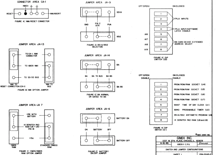
Fi9ure A Sheet 1, of the switch Qnd Jumper confi9uration drawins5 shCows the pinouts of the RESET/tJMI connector (CA-1).
CHMIX, INC. .
4-The GIMIX 6809 CPU sives the use~ the option of selecting
either- a 1, 1.5, or- 2 MHz. oper-atin9 speed fl)r- the (:':~:O':;J. !,lost standard versions of the 6809 will function at either 1 o~ 1.5 MHz. The 2 MHz. 6:;::B09 is r-e9uir-ed fClr- oper-ation at 2 I'1Hz. Note: the al:tual input to the 6809 is 4 times the oper-atins speed. Thus a 1 MHz. 6809 re9uires a 4 MHz. input clock frequency etc. CPU speed is selected by -the position one of the Jumper blocks at Jumper ar-ea . ..IA-8. ...lA-=:;: alsc. deter-milles the clock speed of the clPtic'flal
9511A or 9512 arithmetic processor(see the 9511A/9512 section of
the manual). Jumper area JA-8 is located to the upper risht of the cir-cuit boar-d between Ie U-·I0 and U--l1.
Fisur-es A thr-oush H: Sheet 3 of the swi tch atld juniper-confisur-ati,:.n dr-awinss show the pinouts and -jumper positions f.:,r-the CPU and arithmetic processo~ clock speeds.
NMI option Jumper ,..lA-I:;:: )
The GIMIX 6809 CPU sives the user- the option of connectins the NMI input of the processor to eithe~ the RESET/NMI connector (CA-l) or- to one (If the 1 ines of the Sf:50/SS50C bus. These opt ions ar-e selected by the p(lsiti(ln o-F the Jumper- bl.:.ck at Juniper- ar-ea ,...IA··l:]. When the NMI to reset c(lnnector option is selected only a switct, or device cl:lnnected to the boar-d th,.-oush the RESET/NMI
connector-eCA-l) can sene rate an NMI. When the NMI to bus option is selected any of the on card devices that ~enerate interrupts, as well as any other boards in the system that a~e connected to the proper bus line, can sener-ate an NMI. In the NMI to bus pr)sition ti,e Nl'"lI input buffer is connected t(l the bus line desisnated NMI on the 8850 blJS and BU:=:Y on the S:;:;50C. . .. Jumper- ar'ea ,...IA-·13 is 1 clcated at the lower left of the circuit board near t~immer resistor R-24.
Fisur-e B: Sheet 1, o-F the switch and .. jumper c,:,nfisur'ati')11 drawinss shows the jumpe~ positi(lns for JA-13.
BA/BA-AND-BS option JlJrflPer- ( JA-·14 )
The 6809 CPU has 2 output lines~ BUS AVAILAB~E (BA) and BUS STATUS (BS) that are used to by other devices in the system to deter'mir,e the status elf the pr-(tcesse·r-. (see the 6809 data sheet for details on decodins BA and BS) Amons other thinss DA and BS are us€:'d by DMA devices to deter-mine when thE' pr-ocessor- has
released the bus to them for DMA operations. To provide
compatibi 1 ity with cer-tairl €:'xistirls 8::;-50
t ..
:.ar-ds the GIMIX 6809 CPUBOARD has provisions for gating DA with BS and placing the
r€:'sultins losical AND of th€:' 2 sisnals on the BA line of the SS-50C
bus. Th€:' BA AND BS position of JA-14 maich€:'s the SWTP
configuration of BAlDS.
Fisure E: sh€:'et 1 of the switch and Jumper confi9uration
GIMIX, INC.
EXTENDED ADDRESSING
The 6809 CPU is capable of addressihs a maximum ~f 64K of
memory space directly. This capability, while sufficient for many
applications, is a limitins factor when larser, especiallY
multi-user/multi-taskins, systems are considered. In order to
e:o<pand the addr-essins capability (If the 6809 the SS50C ,bus
definition includes 4 extra or extended address lines. These
additional lihes sive the bus a total of 20 address lines and allow for UP to 1 MBYTE of address space. Since the 6809 senerates only
16 address lines, some combination of hardware and software must be
used to simulate the extra 4 sisnals. NOTE: In order to take
advantase of extended addressins the devices to be addressed must be capable of decoding all 20 address lines. Boards such as the
GIMIX 32K STATIC RAM board. 8 PORT SERIAL I/O board,and 128K
PROM/ROM/RAM board have the capability to decode all 20 Qddress
lines and can be used with extended addressins. The GIMIX 6809
CPU also provides extended address decodins for the 8 devices
decoded b~ the FPLA.
The GIMIX 6809 CPU has provisions for three methods of
simulatins the 4 extra address lines. These methods include
STRAIGHT BANK ::;;ELECT, whict, uses a simple latch, and two differ-ent
methods of Dynamic Address Translation (DAT) which can also
senerate the 4 extended address sisnals. Each method has
advantages and disadvantases and it is UP to the user to determine
which method best suits his needs. In addition, some software
available from various vendors may require that a particular method be used.
STRAIGHT BANK SELECT
I n the s tr-a i sht bank se 1 ect methcld of extended add/-ess i ns the 1 MBYTE of available address space is divided into 16 sections or banks of 64K each. Any devices in the system that a~e set UP to
decode a particular bahk address will only appear on the bus when their bank address apears on the extended address lines of the bus. For example if a multi-user system were being set UP in which each
of three users was to have 32K of memory dedicated to his use, three 32K memory boards could be installed in the system. Each of the 3 boards could be set to the same base address es. $0000-$7FFF
but with each set to a different bank. When a particular user was
to have access to his portion of memor~ the monitor/super~isor
prosram would place the bank address of that user on the extended addr-t?ss bus and his bank (If IT,E'n,(lr-Y wO'Jl d be enat.led. Areas elf memory and devices such as I/O, disk controllers etc., that were to
be sha~ed by all users, would be set to ignore the extended
address lines and would appear at the same address in all banks. While this m~thod is relativelY simple and straightforward i t l , a s
limitations. For example it requires that eac~ user or task be
en
M I X, INC:.-1-::'-
(.::::(>':'-' CTU BOArmis unavailable to other users unless the hardware confi9uration is chansed. Also since it may only be possible to assign an entire board to a particular bank, memory may be wasted because a full 32K must be assigned to a UStor- whc, oril--( r-e9IJir-es lc.K.
BANK SELECT LATCH
When using the STRAIGHT BANf< ::ELECT method addressing, the data on the extended address lines is the value stored in the BANK SELECT LATCH.
clf extended Jet e r-In i ned by
The bank select latch is a write only device that aFFears at memor-· ... - lClcatiorl $FFFF. A pr'ocessor- wr·ite to this 1 (lc.ati(ln stol-es d a t a i nth e 1 at c h • A r- e a d f r' 0 m t his 1 0 cat ion r' e t u r- ... s d a t a f r-0 HI an
--,--other device addressed at this location. Normally a read from this
location would return the restart vector stored in a PROM/ROM
monitor located from SFFFF down. The least significant 4 bits
written to the latch are the bank number SO-SF of the bank to be tonabled.
Any software that
latch must be located in
switching banks. In
modifies thE; contents an
mClst
area of memory that applications bank
of the bank is not
s wit chi n 911) 0 IJ 1 d done by a monitor/suFervisor pr09ram located in memory shar'ed all users and not affected by the extended address lines.
b--(
be
b-'I'-Note: 2 of the remaining bits of the latch are used to control (I the r' fun c t ion 5 .. HI the b (I a r- d • I f e i the r' (I f the s e fun c t i (I n 5 a r- e i II
use any prosrams that modify the bank select latch must not
inadvertently change these 2 bits. Since the bank select latch is a write only device the last data written to the latch should be kept in temporarY storage for comparison when new data is to be written. Bit 5 of the bank select latch is the software control
latch for the FPLA address deco~er and bit 4 controls the user
de fin e d 1 at c h 0 u t put at sol de r' pad " A " • :::; e e the a p p r' 0 p ria t e
section of the manual for further information on these features.
DYNAMIC ADDRESS TRANSLATION (DAT)
Dynamic address translation is a method of m~morY management
that allows better utilization of the memory resources within a
system. It overcomes some of the disadvantases of the strai9ht bank select method of extended addressin9. in that i t allows available memory to be allocated among users as their requirements vary. It
also allows memory boards that can only be addressed as lar9~
con tis u 0 usb 1 0 c k s t 0 bee f f e c t i vel Y s p 1 i t i n t (14K s e s rr .. ", n t E. t t. at can
be addressed as required. Since this re-location of memory is
under software control it can be done at any time and does not
re9uire hardware changes in the system. DAT breaks the, entire
mefTlor-Y space irltc. 4K segments. so m~mor-'{ as'sisflfllt'flt carl IT,or'e closely fit the requirements of each user/task. DAT has st'veral
other advantages, for example, the system mo~itor/ ,Supervis6r
program could tt'st each 4K segment of ffit'ffiOrY before assisning it to
(; I M I X 7 INC. -·7·- (.:::0';;- CPU BOARD
eliminated from the table of available memory and a sood sesment
substituted. The monitor/supervisor prosram could then set a flas
or indicator to show that the system re9uires maintenance.
In order to understand how dYnamic address translation works
we must first understand the concept of physical and losical
addresses. A physical address, as the name implies, is the address
at which a device (memory,I/O,etc.) is set by its hardware to
respond. For example the DIP~switches on a memory board determine
its physical addre~s. A losical address is the address that the
processor outputs when it attempts to access a particular memOr'( location. For example when the processor attempts to write data to location SOOOO it outputs the losical address SOOOO on its address lines. In a system that does not have dynamic address translation the address lines from the processor are connected directly to the bus arId the phys i ca 1 and los i ca 1 addr'ess ar'e a 1 wa","s e"lua 1 • When the pr,(.cessc.r· writes tc. 1 (.cati.:.n $0000 the memor·y at $0000
responds. Dynamic address translation allows us to assisn
different l09ical address to memory that has a particular physical address. For example memory with a physical address of $0000 m~sht
be assi9ned the 109ical address $2000. When the processor attempts to access memory at losical address S2000 the memory at physical address ~OOOO would respond. DAT then is a method of translatin9 the l09ical address from the processor to a physical address that appears on the bus.
DAT is implemented on the GIMIX 6809 CPU board by insertins a high speed. random access memory(the DAT RAM) between the upper 4 address lines of the 6809 and their correspondin9 bus buffers. A second identical RAM is used to generate the 4 bi~s of the extended
address. The 4 address lines from the processor are used to
address 1 of 16 locations in the DAT RAM and the data stored in'
these l6cations becomes the phYsical address that appears on the
bus. The DAT RAM translates the upper 4 bits of the processors
logical address into the upper 4 bit~ of a physical address and 4 bits of extended address. Since the DAT only translates the upper 4 bits of address it divides the memory space into 16 4K losical
se9ments. The physical address space consists of 16 4K physical
address segments in each of 16 possible banks or a total of 256 possible 4K physical address segments. By placing the proper data in the DAT RAM any of the 256 physical se9ments can appear at any
of the 16 109ical address se9ments. For example 4K of memorY
phys ica 11 Y addr'essed at $OOOO-SOFFF c.)U 1 d appear' to' the pr'ocessor'
to be addressed at SCOOO-SCFFF. A physical address segment could
also be made to appear at more than one logical address. For
example a ,4K se9ment phYsically addresed at $EOOO-SEFFF could
appear at SEOOO-SEFFF and SCOOO-$CFFF at the same ti~e.
NOTE: ON POWER UP THE DATA IN THe DAT RAM AND THEREFORE LOGICAL
ADDRES:SES ARE UNDEF I NED. ONL Y THE UPPER 256 BYTES OF MEMORY
SFFOO-SFFFF ARE GUARANTEED TO BE AT THEIR PROPER ADDRESS. IN
SYSTEMS THAT USE DYNAMIC ADDRESS TRANSLATION THESE BYTES MUST
CONTAIN. IN ADDITION TO THE RESET AND INTERUPT VECTORS SOFTWARE
THAT INITIALIZES THE DAT RAMS TO A PREDETERMINED STARTING
CONFIGURATION. THIS HHTIALIZATION MUST TAKE PLACE BEFORE ANY
GIMI X, INC.
AC:CES::;E::; C)UT::: I DE TI-! I!:; 256 BYTE AnEA ARE t1ADE.
For the purpose of writins data to the DAT the DAT RAM shares
the upper 16 bvtes of address space $FFFO-SFFFF with the memory
normallv at these addresses ( usuallv the svstem monitor
PROM/ROM). The DAT RAM is write onlv, a write to these locations stores data in the DAT RAM~ a read from them returns data from the PROM/ROM monitor. The least sisnificant 4 bits of data written to the OAT are stored in the RAM that translates the upper 4 address lines of the 6809, the upper 4 bits are stored in the RAM that Benerates the 4 bits of e~tended address.
Two different methods of dvnamic address translation al-e
available as options on the GIMIX 6809 CPU board. One is
cOlTlpatible with the method used on the ::;;l.JTP MP--09 b(.ar-d and the SWTP SBUG-E monitor ROM. When the board is confiBured for this OAT method the SWTP SBUG-E ROM can be pluBBed directly into the GIMIX 6809 CPU board. The GIMIX 6809 can be ~sed as a direct replacenlent for the SWTP MP-09 board in svstems where baud rates are available from a source other than the CPU board. The GIMIX 6809 CPU does not have an on board baud rate senerator. The second OAT method
is an enhanced version that allows much faster operation when
switchins tasks.
While dynamic address translation lTIay find some use in smaller svstems (64K and under).it will probablv be most useful in larser
multi-user multi-taskins applications. For example, in the system
described in the section on straisht bank select, with 3 users in a
multi-user application, each user (task) could be assisned the
memorv required from anv of the available memory in the sYsteln. As the users memorv requirements chansed memorv could be allocated or
deallocated as necessarv. With the SWTP compatible DAT switchins
users ( tasks> requires writins a new set of 16 values into the DAT RAM each time the svstem switches between users (tasks). With the GIMIX enhanced DAT method the DAT values for UP to 16 different
users (tasks) are written to the OAT RAM and switchinsbetween
users is done bv writins a sinsle byte to a task select resister. Each time the svstem switches users (tasks) onlv the task select resister byte need be written.
SWTP compatible DAT
To use this version of DAT the user must write values to 16 locations in the DAT RAM. Each of the 16 locations cor~esponds to
one of the 16 possible 4K logical add~ess segments. The first
location SFFFO co~responds to 10sical add~e5s segment $OOOO--$OFFF the secc.nd SFFF1 to 51000-51FFr and so (·r. UP te. thE' H_. tho at
$FFFF which corresFonds to l09ical address se~ment SFOOO-SFFFF.
The least sisnificant 4 bits of data written are the COMPLEMENT of
the UFPer 4 bits of the desired Fhysical address. The UFFe~ 4
GIMIX, INC. (:,::::0 '?", CPU BOARD
memory located at phYsical address $2000 in Lank 1 is to appear at losical address SOOOO then the value 51D would be written to the
DAT RAM at location SFFFO. The 1 indicates that the d~sired
sesment is phYsically located in bank 1 and the D is the complement of the upper 4 bits of its physical address, 52000. The following
table shows the 16 losical address sesments with their
correspondins DAT locations, sample data and the resultins physical addresses: LOGICAL ADDRE:3:3 50000-$OFFF $1000-S1FFF 52000-$2FFF S:3000-"$~:FFF $4000--$4FFF $5000-$5FFF $6000-$6FFF S7000-S7FFF $:3000--$!:::FFF S-:;'OOO-S9FFF SAOOO-$AFFF SBOOO--$BFFF $COOO-$CFFF $DOOO-$DFFF $EOOO-$EFFF $FOOO-SFFFF DAT LOCATION SFFFO SFFFl $FFF2 SFFF:3 $FFF4 $FFF5 SFFF¢, $FFF7 SFFF:::! SFFF9 $FFFA SFFFr: SFFFC SFFFD $FFFE $FFFF DATA SOP SOC SOD SOC SlB S09 SOA SO::: S07 " SOC:' S05 $04 SO:3 S02 SOl SOO
NOTICE THAT IN THE ABOVE TABLE:
BANK
o
o
o
o
1 (Io
o
o
o
(>o
o
o
o
o
PHYSICAL ADDRE::;;:=; ::;EGMENT $OOOO-SOFFF t,1000-$lFFF $2000--S2FFF $:3000-- !t:::!Frr S4000--$4rFF !t600(l-!t6FFF S5000-$5FFF 57000--$7FFF S::::OOO- S:]FFF S9000-S';"FFF $AOOO--$AFFr-S[:OOO: SDFTF $Coo(J-$Cn:r SDOOO--SDFFF SEOOO--- SEr-FF $rOOO-$FFrT1 TfE FIRST 4 ENTRIES THE LOGICAL AND PHYSICAL ADDRESSES ARE EQUAL 2 THE FIFTH ENTRY THE PHYSICAL SEGMENT IS IN BANK 1
~! THE :::; I X TH AND SEVENTH ENTRY::;; J-:AVE THE I R F'HY::;; I CAL AND LOG I CAL ADDRESSES REVERSED.
4
n IE REM A I N I NO ENTR I ES ALL HAVE PHYS I CAL AND LOG I CAL ADDRES:::;E::; Ef.!U?
GIMIX enhanced DAT
In this version of DAT the user can write UP to 16 sets of 16
values each to the DAT RAM. Each of these sets of values is
functionally equivalent to the 16 values written to the SWTP
compatible DAT. Each of the 16 sets represents the OAT
confisuration for- orle user or task. Ollce t_he r"e9uired values for all the users (tasks) are written to the DAT a sin91e write to the
task select register is all that is re9uired to switch L~tween
users (tasks). The 16 locations of the DAT RAM appear at the same memory locations as in the SWTP compatible DAT. Before wr-itin9 to the DAT. the number ( SO-SF) of the particular user (task) to be
written must be stored in the task select resister. After the task number is written to the task select register, the 16 DAT values
for that user (task) can be written to the DAT. To completelY
[image:9.635.51.590.39.792.2]CHMI X, INC:.
-10--the GIMIX enhanced DAT the software must write each of the 16 task
numbers to the task select re~ister, in turn, followed by the 16
DAT values for that task. The task select register is located at
SFF7F and like the DAT RAM shares its location with other devices.
The task select re9ister is a write only device and its 109ical and physical addresses are always the same.
As in the other version of DAT the least si9nificant 4 bits of
data written to the DAT correspond to the most si9nificant 4 bits
of the desired physical address, however in the GIMIX Enhanced DAT
these bits need NOT BE COMPLEMENTED. They are the true value of
the upper 4 bits of the desired physical address. The most
si9nificant 4 bits written to the DAT correspond to the bank
address of the desired phYsical se9ment (bank numbers SO-SF). The
least si9nificant 4 bits written to the task select resister
determine which of the 16 tasks ( SO-SF) is active.
Any software that modifies the contents of the task select
resister must reside in memory that will not be affected by the
switchin9 of tasks. It is also ilflPortai"lt to nClte that :2 of the
remainin9 4 bits of this resister are used to control other
functions on the board. If these functions are in use any pro~rams
that modify the contents of the task select re9ister must not
inadvertently change these bits. Since the task select re9ister is
a write only device the last value stored should be maintained in
terTIPOf-ar'Y stor-age for- compar-ison pIJr-po!;;-es when new data is to be
written to the re9ister. Bit 5 of the task select resister is the
software control latch for the FPLA address decoder and Lit 4
contr'ctls the IJSer' defined latch .:IIJtPIJt at sa:alder' Fad "A". See the appropriate sections of the manual for further information on these featur·es.
MEMORY MANAGEMENT CONFIGURATION
The GIMIX 6809+ CPU can be confi9ured for any of the three
merrle.f··''- management techni"lIJes ::;:TRAIGHT BANI::: :::;ELECT, :3WTF'
compatible DAT, or the GIMIX enhanced DAT ) by the installation of
the proper inte9rated circuits at specific locations on the board.
If the board is ordered with one of the two DAT confi9urations, i t
is shipped with only the proper parts for that DAT confi9uration
installed.
If neither DAT is ordered the board is shipped with only the
par·ts for' the STRAIGHT BANI< SELECT installed. If the user- wishes
to change the confi9uration of the board, he can obtain the
necessary parts and install them at any time. The followin9 chart
shows the parts required and their board locations for each of the
three confi9urations. Refer to the component layout drawin9 for
the locations of the sockets on the board.
LOCATION SWTF' COMPo DAT GIMIX DAT BANK SELECT
en
11 I X , I hlC.IJ-22
1)-2:3
1j-37 U-:39 U-40 U--43 U-44 U-45
-11-EMPTY
74L~;174
8T26
<*>
74:31:39
74S1E:9
EMPTY
:=:T28
EMPTY
9::::L422
74L~=;174
::;:T2B EMPTY EMPTY EMPTY
EMPTY
EMPTY Et1PTY
EMPTY EMF'TY
74L::;174
EMPTY
*
An BT26 buffer is re~uired for compatibility with the SWTP DAT and SBUG-E .NOTE: For proper operation, ICsat locations ~arked EMPTY must be removed or relocated when changing configurations.
SOFTWARE WRITE PROTECT
The GIl'lIX 6:30';1 CPU gives the u::.er the abi 1 it,' to write Frotect under' s(.ftwar-e cont.-ol any of the 4:~ Ff",--sical se9rr.ents o-F merr,e·r..-space. The software write protect option uses the most si9nificant bit of each location in the DAT RAM and limits the maximum address
space to 1/2 MBYTE. This bit which normally controls extended
address line A19 is used to inhibit proc@ssor writes to selected 41( sesments. A Jumper option permits setting address line A19 either hish or low so that either the lower 8 ban~s $0-$7 or the UFPer- 8
banks S8-SF can be used. This option can be used only i~
conjunction with 1 of the 2 DAT methods. To write protect a
sesment a 1 must be written to the most sisnificant bit of the DAT
when the selected sesments physical address is written. A 0
written in this position indicates memory that is not write
protected. NOTE: When the board is confi9ured for the SWTP
compatible DAT this pattern is inverted i.e. a 0 is written to
write protect a se9ment and a 1 is written for a segment that is write enabled. This feature will write protect any tvpe of device
including RAM, 1/0 devices, ETC. However, it onlv protects these
devices fr'(lm wr·i tes i:r'om the 6809, it dCles not pr-otect then, fr'on, writes bv other devices that can take control of the bus such as DMA disk controllers etc.
CAUTION: If the software write protect feature is enabled some
existins software for the SWTP compatible DAT mav accidentallv
write protect areas of memory. The software write protect feature can not be used with the SWTP SBUG-E monitor.
Software write protect option Jumper ,.JA-10 )
The software write protect option is enabled by the position of the Jumpers at JA-10. This Jumper area also selects the upper or lower 1/2 MBYTE of addr~ss space when Software write protect is
enabled. JA-10 is located near- the center of the board abo~e
DIP-swi tt:h S2.
Figures J throush
M:
sheet 2 of the switch and Jumperconfisuration drawin9s show the pinouts and Jumper positions for
131 MI X, INC. -12- I':.::::(l';J CTtI BOARD
USER DEFINED LATCH OUTPUT
Th~ device used for the TASK SELECT REGISTER or the BANK SELECT LATCH depending on which memory managemant option is installed, can store 6 bits of data. Since only 5 of these bits are used by the board, the sixth bit is available as a user defined output from the board. This output is available for external connection at solder' pad "A", located below the batter·y ( B...:.l ),
b~tween U-2;;: and U-24. (see the conlPonent 1 a·· ... out dr'awi ng) The
output is IlLS" TTL compatible and is capable of driving an equivalent load. The status of the user defined output is determined by data written to bit 4 of either the TASK SELECT REGISTER or the BANK SELECT LATCH depending on which is installed. I f a l i s w r' itt e nth e (. u t put at pad II A II W ill be h i 9 h , w hen a (> i s
written it will be l(.w. Th-e (flJtPUt of the user' d-efirled latch c(luld b-e us-ed in a variety of ways. For e~amFle,
driv-e an ext-ernal indicator ( LED, buzzer',
. ....
1 I. COIJld t ( . etc. ) to indicate some internal condition of
could als~ b-e used, if wir-ed correctlv, as control latch input to the FPLA address decod-er.
the s·(stefll. It a second software
::;:oftIi.1ar·e either bi ts in
that uses th-e user defined latch must not modifv the the TASK SELECT REGISTER,or BANK SELECT LATCH if thev are being used. See the appropriate sections of the manual for details on the bit positions in the TA::::I< !:::ELECT REOI!;::TER and BANI< SELECT LATCH, and the precautions re9uired for software that writes
to them.
ON CARD DEVICE SECTION
FPLA Address Decoding:
Address decoding for the eight on card devices ( 4 PROM/ROM/RAM sockets, 5::::167 Time oi: Day Clock, 6:340 F'r·c.gammable
Timer, 9511A/9512 Arithmetic Processor and th~ on boafd RAM) is controlled by a Field Programmable L09ic Array (FPLA). The
address~s occupied by each of the 8 devices are fixed bv the
pro9rammin9 of the FPLA. The FPLA has sixteen input lines and eight output 1 ines arid can be pr'ogr'amrrlE-d for' UP to for·tY-eight
different input to output combinations. Twelve of the input lines ar'e connected to addr'ess 1 irles A4 .- A15 thus E-nabl irlg the FPLA to decode address ranges as small as 16 bvtes. The remaining 4 inputs are connected to DIP-switch S2. sE-ctions 1 though 4. Sections 1
-3 directly control their respective FPLA inputs. An ON (closed) switch equals a l09ical 0 to the FPLA. an OFF (open) switch e~uals
GIMIX, INC. -1 :;::-- t.::;:09 CPU BC)ARD
latch inputs allows both hardware and software selection of address decoding for the on card devices.
Each of the 8 FPLA outputs connects to the select logic of one of the 8 on card devices. Each device also has a separate disable switch, DIP-switch S1 sections 1 throush 8. that can be used to
disable that device regardless of the FPLA programming. When a
device is disabled by these switches its address space is available for use by other devices.
The FPLA supplied with the GIMIX 6809 CPU BOARD is programmed
with several different addressing combinations. Combinations are
includ~d for several different existins PROM/ROM monitors. Other
confisurations are included which may be useful in special
applications such as dedicated systems and monitor and system
design. An addressing combination is selected by the settings of
the FPLA input switches S2 (1-4) and the software control latch if enabled. A table is included with this manual that lists each of the addressing combinations available in the FPLA as well - as the
re~uired switch and latc~ settings for each combination. Since one
of the inputs to the FPLA can be controlled by software. is i t
possible to select between two different monitors under software
control. It is also possible to install static RAM in one or more of the PROM/ROM/RAM sockets. load a monitor into it from disk and switch to the RAM monitor from the resident PROM/ROM monitor. This feature is very useful when writing and debugging a custom monitor or when it is desirable to easily and rapidly switch between a variety of different monitors. Since the upper 256 bytes of memory
$FFOO through $FFFF are shared with the DAT, RAM addressed at
between these locations can not be written to.
NOTE: The FPLA is a fusible link programmed device
speciale~uipmentto program. Contact GIMIX. INC.
on custom configurations to meet your re~uirements.
FPLA SOFTWARE CONTROL LATCH
and r- e ~ u i r- e s for- i n for- ma
t
i .:. nWhen the board is configured for either of the 2 dynamic
address translation methods the FPLA latch is controlled by writins
to bit 5 of the task select resister located at $FF7F. When
configured for straight bank select the latch is controlled by
writing to bit 5 of the bank select latch at $FF~F. The FPLA
control latch shares these locations with the task/bank select
functions and the user defined latch output. Programs that write
to the FPLA latch must not inadvertently modify the other bits at these locations. Since the latch is a write only device the last
value written should be kept in temporarY storage for comparison
p IJ r- p c. s e s w hen new d a t a i 5 t c. b"" w r' i t t en. ::; e e t h -;? a p p r-0 p r- i ate
sections of the manual for more information on the task/bank select
functions and the user defined latch output. Since changing the
FPLA latch bit when the latch is enabled. DIP-switch 82 section 4 is ON (closed), may change the address of devices decoded by the FPLA, software that modifies this bit must be located in an area of memory that is not affected by the"change.
C. I M I X , I NC • 14
--Extended add~ess decoding is provided to allow the eight FPLA decoded devices to respond to va~iou5 combinations of the extended
address lines as well as the ~egula~ address bus. An additional
decoding circuit called the Fxxx decoder is also available on the
board. The extended add~ess decoder detects a match between the
address present on the extended address lines ( A16 - A19 ) and the extended address set by sections 5 th~ough 8 of DIP-switch 82 (82 5-8). The Fxxx decode~ detects the presence of an F on the upper 4 lines of the add~ess bus ( A12 th~ough A15). Its output
is t~ue any time a a read o~ write takes place to the upper 4K of
memory (SFOOO-SFFFF). The outputs of these decoders can be
combined in various ways by the arrangement of the programming
Jumpers at Jumper area JA-l1. And used to selectively enable the FPLA address decoder.
NOTE: The extended add~ess decoding, with some exceptions as
descr ibed later, affects all of the devices dec(,ded by the r-PLA.
Figures A through G sheet 2 of
confi~uration diagrams show the pinouts
positions for the various combinations.
the of
SLui tch and
.JA·l1 and the
.j umpe r
.j UITIPer·
The following table lists the combinations that can be
selected by the Jumpers at JA-ll.
#1 FPLA always enabled (extended address and Fxxx decoders disabled). #2 Only devices add~essed by the FPLA between SFOOO and SFFFF are
enabled regardless of extended address.
#3 FPLA only enabled when the extended address p~esented on the bus matches the address set by the extended
addr·ess swit,:hes <:::;2 5--En. *
#4 Devices add~essed by the FPLA between $FOOO and $FFFF a~e always enabled. Devices add~essed below $FOOO respond only when the extended add~ess matches.
#5 Only devices addressed by the FPLA between $FOOO and $FFFF a~e
enabled only when the extended address matches.
#6 FPLA always disabled.
In a singleuse~ application whe~e extended addressing is not
used jumpe~ a~ea JA-l1 would no~mallY be set fo~ configuration 1 (
FPLA always enabled ). Configuration 2 effectively disables all
devices add~essed by the FPLA below $FOOO. When configuration 3 is used devices cont~olled by the FPLA only appear· on a single bank
as set by the extended address switches. ConfigUration 4 allows
devices add~es5ed by the FPLA between $FOOO and $FFFF to appear in
all banks while those addressed below SFOOO only appear in 1
specific bank. This configuration could be used fo~ example in a
bank select system whe~e the system monitor and scratchpad RAM
would appear in all banks while the othe~ devices would only appea~
in a specific bank. Configuration 5 effectively disables all
devices addressed by the FPLA below 'FOOO and only enables devices
addressed between $FOOO and SFFFF when the extended address
GIMI X, INC.
-15-EXTENDED ADDRESS SELECTION
The extended address for the FPLA decoded devices is
determined by the settin9 of DIP-switch S2 sections 5,6,7. and 8 ( 825-B). S2-5 cor-r-esPclnds to the least si9nificant bit (A16) clf the extended address lines and S2-8 to the most si9nificant (AI9). These switches must be set to the binary equivalent of the desir~d
extended address. When the board is confi9ured for either STRAIGHT
BANK SELECT or GIMIX ENHANCED OAT a switch that is ON (closed)
corresponds to a 1 in the apprropriate bit position of the
extended address, a switch that is OFF (open) corresponds to a O.
When the SWTP compatible DAT is installed the switches are
inverted, ON (closed) corresponds to a 0 and OFF (open) to a 1.
The followin9 dia9ram shows examples of extended address settin9s
for S2 5-8 with both GIMIX ENHANCED DAT / STRAIGHT BANK SELECT and the SWTP compatible DAT.
S2 GIMIX DAT /
SECTION BANK SELECT
c-~I ON
6 OFF
7 OFF
,-,
Co OFF
SWTP compo DAT
OFF ON ON ON
EXTENDED ADDREES:':; SET FCm BANI< $01
GIMIX OAT /
orF
ON ON OFF:':;WTP COMPo DAT
ON OFF OFF ON
EXTENDED ADDRESS SET FOR BANI::: $O.~,
NOTE: The settin9 of the extended address switches is only
necessary when Jumper area JA-ll is set for one of the
confi9urations that use extended addressin9. Configurations 3,4,
and 5 use the extended address decodin9 and DIP-switch 52 sections
5 throu9h 8 must be set to the desired address. Confi9urations
1,2, and 6 i9nore the extended address and the switch settin9s.
See the EXTENDED ADDRESS DECODING section for details of these
confi9ur-ations.
PROM/ROM/RAM SOCKETS:
The board has four 24 pin ~ockets ( U-4,5,6, and 7 )that can accept most 2708/2716 pinout compatible, 1 to 8K byte PROM/ROM/RAM
devices. Either sin9le or multiple supply voltage parts can be
used and each of the four soc~ets can be individualy Jumper
pro9rammed for device size and type. Jumper areas located above
each socket ( JA-2,3,4.and 5) rearrange the pinouts of the sockets as required for the various devices. The device size and address location for each socket is determined by the pr09rammin9 of the FPLA address decoder. (see the FPLA SEction of the manual and the
FPLA DATA sheet for information on device size and address
locations). Custom programming of the FPLA allows an ~lmost
unlimited number of combinations to be used ( please contactGIMIX
for information on custom FPLA programmin9 if your application
GIMIX, INC.
-I/.:.-The PROM/ROM/RAM Jumper configurations drawing shows the
pinouts of the Jumper areas and 9ives examples of Jumper positions
for the most common devices that can be used. GIMIX will provide,
on re~uest, information on the suitability and Jumper pro9rammin9
for devices not listed on the drawin9.
Each of the 4 PROM/ROM/RAM sockets can be individualy enabled
or disabled bv DIP-switch Sl sections 1,2,3, and 4. When enabled a
socket occupies the address space determined for i t by the FPLA and
when disabled that address space is made available for other
devices in the system. The sockets are enabled when their
associated switch is ON(closed) and disabled when i t is OFF(open).
Sections 1,2,3, and 4 correspond to sockets U-4,5,6, and 7
respectively. :3ee fi9ur'e 1-1= sheet 1 of the switch and .jumper
confi9uration drawin9s.
The speed re~uirements for devices installed in the
PROM/ROM/RAM sockets depends on the speed of the CPU. When
operatin9 at 1 MHz. devices with an access time of 615 ns. or
les5 are re~uired. 1.5 and 2 MHz. operating speeds re9uire 360 ns
or' less and 240 ns. or' less devices r·espectivel··.... NCnE: Thes<Ec'
fi9ures take into account d<Ec'lays intrQduced bv the DYnamic Address
Translation RAMs. In systems that do not use the DAT the fi9ur<Ec's
can b<Ec' increased by approximatelv 40 ns. For example without DAT a
IMHz. system r<Ec'9uires devices with an access time of 655 ns. or
less.
SCRATCH PAD RAM
The board has provisions an optional lK bvtes of scratchpad
RAM. The 2 sockets( U-8 and U-9 } will accept anv 2114 compatible
RAMs includin9 CMOS types and has provisions for batterv backup of
this RAM when CMOS devices are used and the time of day clock with
batterv backup option is installed.
The addressin9 of the scratchpa1 RAM is determined bv the FPLA
address decoder (see the FPLA section of the manual). The address
at which the RAM appears dep<Ec'nds on the programming of the FPLA and
the settin9s of the FPLA input switches and software control
1 atch.
The scratchpad RAM can be disabled by DIP-switch SI section 8
(Sl-8). When this switch is ON(closed} the RAM is enabled as
determined by the FPLA. When Sl-8 is OFF(open) the RAM is disabled
and can rl(.t appear in the addr·2ss space. See figur'e 1-1: sheet 1 of
the switch and Jumper confi9uration drawin9s.
If 2114 e~uivalent CMOS parts are installed at U-8 and 9, and
the battery backup clock option is installed, Data is retained in
th'2 5cratchpad RAM when the sYsterrl Fower is turned off.
Th.:-NMOS/CMOS RAM option Jumper JA-7 connects the U-8 and 9 to either
the regular +5 volt supplv or to the batterv backuF sUFFlv.
CAUTION: JA-7 MUST NOT BE SET TO THE CMOS POSITION UNLESS CMOS
MEMORYS ARE INSTALLED When the JA-7 is set for CMOS RAM and the
CiIMIX, INC.
-17-9 ar'e alwa· ... ·s pOuH:~r'ed, even if the b.;:,ar·d is r'eITI')v<2d fr'om th<2 s·· ... steHI. BE SURE THAT THE BATTERY .JUMPER .JA-;~. I:::; IN THE CWr- PC):::;ITIOtJ OR T:lAT
JA-7 IS NOT JUMPERED FOR CMOS RAM BEFORE REMOVING OR INSTALLING
PARTS ATU-8 and 9. Jump<2r areas JA-6 and 7 are located in the
upper risht corner of the board to the left of the batterv. See
fisures C and F: sheet 1 of the switch and Jumper confisuration
drawings for the configuration of these Jumpers.
To insure data intesritv, an unsafe voltage detect circuit
inhibits all write operations to the scratchpad RAM when i t senses
the loss of system power. This prevents false writes to the RAM
during the transition from svstem to batterv and batterv to svstem
power, wh<2n the batterv backup option is used.
9511A/9512 Arithmetic Processor:
E i the r' t h <2 9511 A 0 r 95 12 a r' e a va i 1 a b 1 e as 0 p t ion s 0 rl the G I M I, X
6809 CPU board. The 9511A/9512 are extr<2melv fast and pow<2rful
devices for performing mathematical calculations. The 9511A
offers 16 and 32 bit fixed-point and 32 bit floatins-point
arithmetic and a varietv of transcendental functions. Thes<2
functions are: Sine, Cosine, Tansent, Arc Sine, Arc Cosine, Arc
Tansent, Square, Square Root, Common Los, Natural log, Natural Anti
Los, exponentiation, and a 32 bit floating PI. The 9512 offers 32
and 64 bit floatins and fix<2d point addition, subtraction,
multiplication and division but none of th<2 transcend<2ntal
functions. The use of th<2s<2 devices can take much of the burden of
mathematical calculations off of the processor. The processor can
load data into the 9511A/9512, issue th<2 necessarv command and then
either poll the status bit of the part or perform other tasks while
waitins for the part to senerat<2 an interrupt. and then r'<2ad th<2
results from the prOP<2r resist<2r.
The 9511A/9512 occupies 16 bvtes of address spaC<2, its addr<2ss
is d<2termined bv the FPLA prosrammins and FPLA input switches and
software control latch. The first bvte is th<2 data resister and
the second bvte is the status resister, for example if th<2
9511A/9512 W<2re addressed from $E200 throush SE20F. Th<2 data
resister would appear at locations SE200, $E202. etc. and the data
resister would appear at SE201, SE203, etc. Both d~vices are stack
oriented and have onlv two 8 bit wide resisters. The data is
~ritten to them 1 bvte at a time, a command issued, and the result
is read from them a bvte at a time.
CAUT I ON: I N ORDER TO MEET THE TIM I NCi F,E()U I F,EMENT::; OF T~ IE
9511A/9512 THE MRDY CIRC::IJITRY OF THE CPU BOARD I:;:; U~::;ED TO ::;TRETCH
THE PROCESSOR CLOCK DURING ACCESSES TO THE DEVICE. BECAUSE OF THE
WAY 9511A/9512 FUNCTIONS IT IS POSSIBLE IF CERTAIN PRECAUTIONS ARE
NOT OB::;ERVED TO GENERATE A MRDY :::IGNAL THAT I:::; LONGER THAN .THE 6:::09
CAN TOLERATE. THIS COULD CAUSE UNPREDICTADLE RESULTS AND POSSIBLY
CAUSE THE ENTIRE SYSTEM TO "CRA::::H". TO AVOID THIS, SOFTWAF'\E THAT
READS THE RESULTS OF A 9511A/9512 OPERATION FROM THE DATA REGISTER
MUST NOT DO SO UNTIL THE DEVICE HAS COMPLETED THE OPERATION. THIS
CONDITION CAN ALSO OCCUR IF A ==;ECOND COMMAND I::; l·JRITTEtJ TO THE
DEVICE BEFORE THE PREVIOUS OPERATION IS COMPLETED .
GIMIX, INC. --1 :::-- (;.::::09 CPU· BOARD
THE COMPLETION OF AN OPERATION CAN BE DETERMINED BY READING THE
STATUS REGISTER OF THE DEVICE OR BY WAITING FOR THE DEVICE TO
GENERATE AN END OF OPERATION INTERRUPT BEFORE ATTEMPTING TO READ
THE RESULT FROM THE DEVICE. THIS PRECAUTION IS NOT REQUIRED WHEN WRITING DATA TO THE DEVICE OR WHEN READING THE STATUS REGISTER.
See the manufactu~ers data sheets and the sample program
listings, included when the 9511A/9512 are facto~y installed, for
info~mation on data for~ats and prog~am requi~ements fo~ thes~
devices.
9511A/9512 clock speed
The clock speed of the 9511A/9512 is totallY independent of the 6809 p~ocessor clock.. They share the same Jumper area (JA-8) for clock speed selection but there are no rest~ictions other than
the maximum operating speed of the parts, on 6809 and 951A/9512
clock speed combinations. For example th~ 6809 can be operated at 1 MHz. while the 9511A/9512 is r-IJnning at :::: MHz or- -the 6::::0';J at 1.5 MHz. while the ':;'511A/9512 is set for- 2 1'1Hz. etc. Cl cick speeds of
2,3, and 4 Mhz. a~e available at JA-8. clock speed fo~ the
device. Various ve~sions of both devices are available with
different makimum operating speeds. Jumper area JA-8 5hould not be set fDr a speed hishe~ than the ratins of the part.
Fisures A throush H: sheet 3 of
confisuration drawinss show the pinouts and .JA-8.
9511A/9512 interrupt selection
the switch and JumFer
Jumper positions for
The 9511A/9512 is capable of seneratins interrupts. The
interrupt output of the device can be connected. b~ JumFer area
JA-12, to anYone of the three 6809 hardware inte~rupt lines ( NMI, FIRQ, and IRQ). NOTE: The NMI line at JA-12 is only active when
the NMI option Jumpe~ ( JA-13) is in the NMI to bus position.
(See the NMI option Jumpe~ section) An additional Jumper a~ea JA-9 must be set ~o eithe~ the 9511A or 9512 position depending on which
part is installed. This jumpe~ is ~equired because of a
diffe~ence in the inte~rupt outputs between the 2 devices. JA-12
is located in the lower left of the board to the lef~ of U-33.
Fi9u~e H: sheet 2 0 f the switch and Jumper confisuration
drawin9s shows th~ pinouts of JA-12. Jumper area JA-9 is located below the 9511A/9512 socket U-3. Fi9u~~ D: sheet 1 of the switch
and Jumper confisuration d~awin9s shows the jumpe~ positions for
,JA-9.
9511A/9512 enable/disable switch
The SI-7 ) • determined
9511A/9512
When SI-7
by FPLA.
can be disabled by DIP-switch 81 section 7 (
is ON(closed) the device is enabled as
en
M I X , I NC •6840 Pro9rammable Timer:
The 6840 Pro9rammable Timer has 3 independent. software
programmable timers that can be used for timing, counting,
freque~cy and period measurement. etc. The 3 timers can be used
independentlY or they can be cascaded in various ways depending on the application. The input. output, and gate connections for all 3 timers are available at a Jumper area (JA-1). This Jumper area can be used with Jumper blocks and/or standard wire wrap techniques to
interconnect the timers, or with the appropriate connector (not
supplied) to connect them to external devices. A 1MHz. clock
output is also available at JA-1.
6840 addr-essing
The 6840 occupies sixteen bytes of address space as determined
by the programming in the FPLA and the FPLA input switches a~d
softwar'e contr'ol latch. The following table ShOliJ5 the b·,..te
assignment with byte 1 being the lowest address assigned to the
device.
B·· ... te 1 Wr' i te R·,..te 2 Write B··,..te "':1 Write
'-'
B··,..te 4 Wr' i te Byte r= ,_I Wr' i te B·'I··te 6 Write B··,..te 7 Wr- i te Byte ,-, c' Wr- itt'
Wr' i te
CClntr'ol Re9 i ster' #1/#3 Contr-o 1 Reg i ster' #2 M:;:;B Buffer' Register T i rr,e r- #1 Latches M::::B Buffer- Reg i s ter' Timer' W-:' ''':'' Latches
MSB BIJffer' Register Timer' #'0;;' '-' Latcht's
nead
No Defined Operation Read Status Register Read Timer #1 Counter Read LSB Buffer Re9ister Read Timer #2 Counter Read LSB Duffer Register Read Timer #3 Counter Read LSB Buffer Register
The remaining 8 bytes art' a repeat of the first 8 bytes listed above, i. e. Byte 9 is the same as Byte 1, Byte 10 is the same a5 Byte
See the 6840 manual
information on the functions the 6840 programmable timer.
6:340 i nter-r-upt s
included of these
with b··,..tes
the boa r' d for' and on programming
detailed and using
The interrupt output of the 6840 can be Jumpered to anyone of the three interrupt lines (NMI,FIRQ, and IRQ) by the programming Jumpers at Jumper area JA-12. NOTE: The NMI line at JA-12 is only active when the NMI option Jumper JA-13 is in the NMI to bus position. (see the NMI option Jumper section) JA-12 is located at the lower left of the board
to the left of U-33. Figure H: sheet 2 of the switch and Jumper
configuration drawings shows the pinouts of JA-12.
6840 enable/disable
(; I M I X, INC. -20-"
81-6 is ONCclosed) the 6840 is enabled a determined by the FPLA. When
81-6 is OFF(open) the device is disabled and its memory space IS
available for other devices in the system.
6840 accurac ... ·
Regardless of whether the 6840 uses the internal clock reference or
an external one, the device uses the (E) signal from the 6809 for
internal syncronization. Since this eEl signal is stretched by the
processor during slow memory accesses using the MRDY line the accuracy of the device may be affected if such accesses (slow memory) are made while the 6840 is counting. Under normal circumstances this effect will be negligible. However. in applications where timing is critical and ~
great deal of slow memory accesses are made this should be ta~en into c 0) n sid e r' a t ion.
58167 Time of Day Clock
The 58167 Time of Day Clock option provides the user with any easy rrleans of keeping time ( secorlds, minutes, l"H.ur=., da:'( (,f week, day of
month, month of year) in the system. It also provides pro9rammable
interrupt capability. The battery backup feature allows the clock to
maintain accurate timekeeping even when the sYstem power is removed.
The device has its own built in oscillator and a separate crYstal and is independent of processor clock speed and timing.
5:3167 addr'es s i rig
The 58167 occupies 32 bytes of address space as determined by the
programmin9 of the FPLA, and the FPLA input switches and software
control latch. The following table shows the byte assignments for the 58167 with byte 1 being the lowest address assi9ned to the device.
B",··te 1 Count'2r'
-
Thousandths of ::;;e c 0 rl dsByte ~,
"'- COIJnter'
-
Hundr'edt h s and Terlths of :=;(?condsByte ':' Counter' ::;;econds
"-'
B··f··te 4 (:0 u n
te
r'-
Mi nute.sB ....
·te
r:::- Counte r' Hour's~I
B' ... ·te 1.:.. Counter' Day of the We,::k
B··..-te 7 C:ounte r' [l,a:·,.. (of th\? Month
Byte ( j COIJnt<2r
' ....
-
Mc(nthsB'·..-te 9 Latches
-
Thousandths. ( I f ::;;e c () fa oj sB"·(te 10 Latches HlJndr..?dths and T..?nths of 8ec()r.ds B· ... te 11 Latches
-
Si!,:ortd~.Byte 1 .-, "- Latches -- Minutes
Byte 1 ,:.
-'
Latch,2S HOIJr'sByte 14 Latches
-
Day of the WeekByte 15 Latches
-
Da"( of the MonthB"·{te 1(:, Latches
-
Me.r. t h:sGH1I X 7 INC.
B··,··t e 18 Byte 19
B ... ·te 20 Byte 21 Byte 22 Byt€
B·· ... te
-,.-.
L"':'
24
*
*
*
-21-Int€rrupt Control Register Coun ter· Re se t
Latch reset !:;tatus Bit
"GO" CClmmand
Standby Interrupt Undefined
*
*
*
Undefined Test Mode
e9ar·d 1 es
6::::09 CPU BOARD
NOTE: Bytes 24 throu9h 31 ar€ undefin€d and not used. They ar€ decoded by the board and ar€ not available for other devices when the 58167 is
enabled.
58167 programmin9
The data format of the time counters ( bytes 1 (binar·y coded decimal), two digits per· byte. These S€t th€ time as well as read time from the device.
thr·ough ::: ) is BC:D
counters are used to The remaining bytes use a binary format and are used to program he devices interrupt output as well as read status,reset the counters, etc. Basically, settins the clock requires resettin9 the counters to zero by writin9 to the counter reset byte (byte 19), storin9 the time in BCD format in the counters MINUTE throu9h MONTH), and then writin9 to the GO byte (byte 22). The 58167 data sh€et included when the clock option is purchased contains detailed information on settin9 the the clock and usins the pro9rammable
interrupts. Sample pr09rams, included with this manual, 9ive examples
of setting and readin9 the clock.
NOTE: THE 58167 HAS A STATUS BIT THAT IS SET WHENEVER THE COUNTERS CHANGE (ROLL OVER) WHILE THE TIME IS BEING READ. THIS BIT SHOULD BE TESTED AFTER A HEAD FROM THE DEV I CE AND THE DATA RE·- HEAD I F THE BIT I:;:; SET. THIS IS TO INSURE THAT THE DATA READ IS VALID. THE STATUS BIT IS CLEARED BY READING THE STATUS.
58167 interrupts
The int€rrupt output from th€ 58167 can b€ conn€cted to anyone of the thr€e 6809 hardware interrupt lines by pro9rammin9 Jumpers at Jumper ar€a JA-12. NOTE: The NMI int€rrupt line at JA-12 is only activ€ when the NMI option Jumper JA-13 is in th€ NMI to bus position. (see the NMI
option Jumper section) Fi9ure H: sheet 2 of the switch and Jump€r
confi9uration drawin9s shows th€ pinouts of JA-12.
Ba tt€r·Y backup
Included with
backup circuit that
- .-. ~ .. -. , ... -. .4
13 I M I X , INC. -22- (:,809 CPU BOAr,[I
be used to retain data in the lK
RAM option is installed.(see the lk
battery backup system consists of a
battery and associated char9in9 and unsafe
This battery circuit can also
scratchpad RAM if the CMOS
scratchpad RAM section) The
rechargeable nickel-cadmium
voltage detect circuitrY.
Batter"", char9in9
The char9in9 circuit charges the battery whenever system
applied to the board and the battery on/off Jumper JA-(:'
battery on position. The batterY used is desi9ned for
chargin9 and can not be overcharged.
power· is is in the continuous
CAUTION: When the battery on/off Jumper is in the battery on
positiofl power· is aFPl ied to the 58167 socket (U·-l) at all tirrtes, even when the board is r·emoved fr·om the systerrl. The same is tr·ue fe,r· ttle 1K
scratc~Fad RAM sockets U-8 and 9, if the CMOS/NMOS RAM option Jumper is
in the CMOS RAM position. (see the 1K scratchpad section) Before
removing or installing parts in these sockets the battery on/off JumFer should be placed in the e,ff positiQn e,r· damage tQ the par·ts may result. The batter·· ... · on/off .jumper· .JA-b is le,cated tel the left of the batter···,··. Fi9ure F: sheet 1 of the switch and Jumper cQnfi9uration drawin9s shows the Jumper Fositions for JA-(:'.
Unsafe voltage detector
The unsafe volt~ge detector monitors the unre9ulated +8 volt supply
from the bus. If the bus voltage falls below a pre-set level the
circuit holds the processor in a reset state ( reset line low) places the 58167 in its PQwer down mode (
PD
low> and inhibits writes to thescratchpad RAM. This prevents false accesses to these devices durin9
planned or unplanned power losses. When the voltage returns to a safe level the reset state is released ( th~ processor perfo~ms its normal power on reset sequence) and t~e clock and RAM are restored to normal c,per·a t i on.
Unsafe voltage threshold adjust
The voltage at which the unsafe voltage detector activates is
determined by the setting of R-24, which is located near the heats ink in the lower- left cor·ner· of the bc'ar-d. This adJustnterltis factor'Y set at a voltage Just above the point where the on board voltage regulators fall
out of re9ul~tion, approximatelY 7.1 volts and should not need
readjustment under normal ci~cumstance5. NOTE: In certain S5-50
systems with mar9inal power supplies. the bus voltage maybe too low to allow proper operation of the GIMIX 6809 CPU board. These systems will
require modifications to their power supplies to provide sufficient
vo 1 tage. The bus vo 1 tage of the s', s telll shou 1 d be somewhat abclve the settin9 of the unsafe voltase threshOld to provide for normal voltage
GIMI X 7 INC.
Normal operation of the GIMIX 6809 CPU board cannot be 9uaranteed if the unsafe voltage threshold is lowered from the factorY setting or
the bus voltage is insufficient to provide proper operation
c i r' cu it.
=:::TARTING ADDRE::::::::
$F800
$F400
$FOOO
$E800
$E400
$E3FC
$E3F8
GIMIX 6809 MEMORY MAP
ENDINf3 ADDRE=;::::;;
$FFFF
$F7FF
$F;;:FF
$EFFF
$E7FF
$E3FF
$E3FB
DESCRIPTION
'3MXBUG-09
VIDEO PROt1 OR USER PROM
USER PROM ( ... l .... COMMAND)
VIDEO RAM (80 X 24)
ON CARD SCRATCH PAD RAM
VIDEO BOARD REGISTERS (80 X
UNDEFINED, AVAILABLE
TO
USER 24)$E3BO $E:3F7 RESERVED FOR FUTURE GIMIX USE
$E:;:A8 $E;::AF GRAPHIC::: CARD
$E240 $E:3A7 UNDEFINED, AVAILABLE TO USER
$E220 $E2;;:F 58167 ON CARD DEVICE
$E210 $E21F 6840 ON CARD DEVICE
$E200 $E20F 9511A/9512 ON CARD DEVICE
$E100 $E1FF UNDEFINED. AVAILABLE TO USER
$E070 $E07F 1/0 PORT 7
$E060 $E06F 1/0 PORT 6
$E050 $E05F 1/0 PORT
c-... J
$E040 $E04F 1/0 PORT 4
$E030 $E03F I/O PORT .-.:.
-'
$E020 $E02F I/O PORT 2
$E010 $E01F I/O PORT '1
$EOOO $EOOF 1/0 PORT 0
$COOO $DFFF USER RAM (GIMIX FLEX)
$0000 $BFFF USER RAM
THIS MEMORY MAP IS FOR GMXBUG-09. THE FOUr< FPLA SWI1CHE.::S ARE IN THE OFF (OPEN) POSITION AND THE PORTS ARE CONFIGURED FOR db BYTES PER I/O ADDRESS.