MOBILE 3D
GRAPHICS SoC
From Algorithm to Chip
Jeong-Ho Woo
Korea Advanced Institute of Science and Technology, Republic of Korea Ju-Ho Sohn
LG Electronics Institute of Technology, Republic of Korea Byeong-Gyu Nam
Samsung Electronics, Republic of Korea Hoi-Jun Yoo
MOBILE 3D
MOBILE 3D
GRAPHICS SoC
From Algorithm to Chip
Jeong-Ho Woo
Korea Advanced Institute of Science and Technology, Republic of Korea Ju-Ho Sohn
LG Electronics Institute of Technology, Republic of Korea Byeong-Gyu Nam
Samsung Electronics, Republic of Korea Hoi-Jun Yoo
Visit our Home Page on www.wiley.com
All Rights Reserved. No part of this publication may be reproduced, stored in a retrieval system or transmitted in any form or by any means, electronic, mechanical, photocopying, recording, scanning, or otherwise, except as expressly permitted by law, without either the prior written permission of the Publisher, or authorization through payment of the appropriate photocopy fee to the Copyright Clearance Center. Requests for permission should be addressed to the Publisher, John Wiley & Sons (Asia) Pte Ltd, 2 Clementi Loop, #02-01, Singapore 129809, tel: 65-64632400, fax: 65-64646912, email: [email protected].
Designations used by companies to distinguish their products are often claimed as trademarks. All brand names and product names used in this book are trade names, service marks, trademarks or registered trademarks of their respective owners. The Publisher is not associated with any product or vendor mentioned in this book. All trademarks referred to in the text of this publication are the property of their respective owners.
This publication is designed to provide accurate and authoritative information in regard to the subject matter covered. It is sold on the understanding that the Publisher is not engaged in rendering professional services. If professional advice or other expert assistance is required, the services of a competent professional should be sought.
Other Wiley Editorial Offices
John Wiley & Sons, Ltd, The Atrium, Southern Gate, Chichester, West Sussex, PO19 8SQ, UK
John Wiley & Sons Inc., 111 River Street, Hoboken, NJ 07030, USA
Jossey-Bass, 989 Market Street, San Francisco, CA 94103-1741, USA
Wiley-VCH Verlag GmbH, Boschstrasse 12, D-69469 Weinheim, Germany
John Wiley & Sons Australia Ltd, 42 McDougall Street, Milton, Queensland 4064, Australia
John Wiley & Sons Canada Ltd, 5353 Dundas Street West, Suite 400, Toronto, ONT, M9B 6H8, Canada
Wiley also publishes its books in a variety of electronic formats. Some content that appears in print may not be available in electronic books.
Library of Congress Cataloging-in-Publication Data
Mobile 3D graphics SoC : from algorithm to chip / Jeong-Ho Woo ... [et al.]. p. cm.
Includes index.
ISBN 978-0-470-82377-4 (cloth)
1. Computer graphics. 2. Mobile computing. 3. Systems on a chip. 4. Three dimensional display systems. I. Woo, Jeong-Ho.
T385.M62193 2010 621.3815–dc22
2009049311
ISBN 978-0-470-82377-4 (HB)
Typeset in 10/12pt Times by Thomson Digital, Noida, India.
Printed and bound in Singapore by Markono Print Media Pte Ltd, Singapore.
Preface ix
1 Introduction 1
1.1 Mobile 3D Graphics 1
1.2 Mobile Devices and Design Challenges 3
1.2.1 Mobile Computing Power 3
1.2.2 Mobile Display Devices 5
1.2.3 Design Challenges 5
1.3 Introduction to SoC Design 6
1.4 About this Book 7
2 Application Platform 9
2.1 SoC Design Paradigms 9
2.1.1 Platform and Set-based Design 9
2.1.2 Modeling: Memory and Operations 14
2.2 System Architecture 18
2.2.1 Reference Machine and API 18
2.2.2 Communication Architecture Design 22
2.2.3 System Analysis 25
2.3 Low-power SoC Design 27
2.3.1 CMOS Circuit-level Low-power Design 27 2.3.2 Architecture-level Low-power Design 27
2.3.3 System-level Low-power Design 28
2.4 Network-on-Chip based SoC 28
2.4.1 Network-on-Chip Basics 29
2.4.2 NoC Design Considerations 41
2.4.3 Case Studies of Chip Implementation 48
3 Introduction to 3D Graphics 67
3.1 The 3D Graphics Pipeline 68
3.1.1 The Application Stage 68
3.1.2 The Geometry Stage 68
3.2 Programmable 3D Graphics 78
3.2.1 Programmable Graphics Pipeline 78
3.2.2 Shader Models 81
4 Mobile 3D Graphics 85
4.1 Principles of Mobile 3D Graphics 85
4.1.1 Application Challenges 86
4.1.2 Design Principles 87
4.2 Mobile 3D Graphics APIs 91
4.2.1 KAIST MobileGL 91
4.2.2 Khronos OpenGL-ES 93
4.2.3 Microsoft’s Direct3D-Mobile 95
4.3 Summary and Future Directions 96
5 Mobile 3D Graphics SoC 99
5.1 Low-power Rendering Processor 100
5.1.1 Early Depth Test 101
5.1.2 Logarithmic Datapaths 102
5.1.3 Low-power Texture Unit 104
5.1.4 Tile-based Rendering 106
5.1.5 Texture Compression 107
5.1.6 Texture Filtering and Anti-aliasing 109
5.2 Low-power Shader 110
5.2.1 Vertex Cache 110
5.2.2 Low-power Register File 111
5.2.3 Mobile Unified Shader 113
6 Real Chip Implementations 119
6.1 KAIST RAMP Architecture 119
6.1.1 RAMP-IV 120
6.1.2 RAMP-V 123
6.1.3 RAMP-VI 127
6.1.4 RAMP-VII 132
6.2 Industry Architecture 139
6.2.1 nVidia Mobile GPU – SC10 and Tegra 139
6.2.2 Sony PSP 143
6.2.3 Imagination Technology MBX/SGX 144
7 Low-power Rasterizer Design 149
7.1 Target System Architecture 149
7.2 Summary of Performance and Features 150
7.3 Block Diagram of the Rasterizer 150
7.4 Instruction Set Architecture (ISA) 151
7.5 Detailed Design with Register Transfer Level Code 154
7.5.1 Rasterization Top Block 154
7.5.3 Main Controller Design 156
7.5.4 Rasterization Core Unit 158
8 The Future of Mobile 3D Graphics 295
8.1 Game and Mapping Applications Involving Networking 295 8.2 Moves Towards More User-centered Applications 296
8.3 Final Remarks 297
Appendix Verilog HDL Design 299
A.1 Introduction to Verilog Design 299
A.2 Design Level 300
A.2.1 Behavior Level 300
A.2.2 Register Transfer Level 300
A.2.3 Gate Level 300
A.3 Design Flow 301
A.3.1 Specification 302
A.3.2 High-level Design 302
A.3.3 Low-level Design 303
A.3.4 RTL Coding 303
A.3.5 Simulation 304
A.3.6 Synthesis 304
A.3.7 Placement and Routing 305
A.4 Verilog Syntax 305
A.4.1 Modules 306
A.4.2 Logic Values and Numbers 307
A.4.3 Data Types 308
A.4.4 Operators 309
A.4.5 Assignment 311
A.4.6 Ports and Connections 312
A.4.7 Expressions 312
A.4.8 Instantiation 314
A.4.9 Miscellaneous 316
A.5 Example of Four-bit Adder with Zero Detection 318
A.6 Synthesis Scripts 320
Glossaries 323
This is a book about low-power high-performance 3D graphics for SoC (system-on-chip). It summarizes the results of 10 years of “ramP” research at KAIST (ramP stands for RAM processor) – a national project that was sponsored by the Korean government for low-power processors integrated with high-density memory. The book is mostly dedicated to 3D graphics processors with less than 500 mW power consumption for small-screen portable applications
Screen images continue to become ever-more dramatic and fantastic. These changes are accelerated by the introduction of more realistic 3D effects. The 3D graphics technology makes vivid realism possible on TV and computer screens, especially for games. Complicated and high-performance processors are required to realize the 3D graphics. Rather than use a general-purpose central processing unit (CPU), dedicated 3D graphic processors have been adopted to run the complicated graphics software. There is no doubt that all the innovations in PC or desktop machines will be repeated in portable devices. Cellphones and portable game machines now have relatively large screens with enhanced graphics functions. High-performance 3D graphics units are included in the more advanced cellphones and portable game machines, and for these applications a low power consumption is crucial. In spite of the increasing interest in 3D graphics, it is difficult to find a book on portable 3D graphics. Although the principles, algorithms and software issues have been well dealt with for desktop applications, hardware implementation is more critical for portable 3D graphics. We intend to cover the 3D graphics hardware implementation especially emphasizing low power consumption. In addition, we place emphasis on practical design issues and know-how. This book is an introduction to low-power portable 3D graphics for researchers of PC-based high-performance 3D graphics as well as for beginners who want to learn about 3D graphics processors. The HDL file at the end of the book offers readers some first-hand experience of the algorithms, and gives a feel of the hardware implementation issues of low-power 3D graphics.
1
Introduction
1.1 Mobile 3D Graphics
Mobile devices are leading the second revolution in the computer graphics arena, especially with regard to 3D graphics. The first revolution came with personal computers (PC), and computer graphics have been growing in sophistication since the 1960s. To begin with it was widely used for science and engineering simulations, special effects in movies, and so on, but it was implemented only on specialized graphics workstations. From the late 1980s, as PCs became more widely available, various applications were developed for them and computer graphics moved on to normal PCs – from specific-purpose to normal usage.
Three-dimensional graphics are desirable because they can generate realistic images, create great effects on games, and enable slick effects for user interfaces. So 3D graphics applications have been growing very quickly. Almost all games now use 3D graphics to generate images, and the latest operating systems – such as Windows 7 and OS X – use 3D graphics for attractive user interfaces. This strongly drives the development of 3D graphics hardware. The 3D graphics processing unit (GPU) has been evolving from a fixed-function unit to a massively powerful comput-ing machine and it is becomcomput-ing a common component of desktop and laptop computers.
A similar revolution is happening right now with mobile devices. The International Telecommunications Union (ITU) reports that 3.3 billion people – half the world’s population – used mobile phones in 2008, and Nokia expects that there will be more than 4 billion mobile phone users (more than double the number of personal computers) in the world by 2010 [1]. In addition, mobile devices have been dramati-cally improved from simple devices to powerful multimedia devices; a typical specification is 24-bit color WVGA (800480) display screen, more than 1 GOPS (giga-operations per second) computing power, and dedicated multimedia processors including an image signal processor (ISP), video codec and graphics accelerator.
Mobile 3D Graphics SoC: From Algorithm to Chip Jeong-Ho Woo, Ju-Ho Sohn, Byeong-Gyu Nam and Hoi-Jun Yoo
So 3D graphics is no longer a guest on mobile devices. A low-cost software-based implementation is used widely in low-end mobile phones for user interfaces or simple games, while a high-end dedicated GPU-based implementation brings PC games to the mobile device.
Nowadays, 3D graphics are becoming key to the mobile device experience. With the help of 3D graphics, mobile devices have been evolving with fruitful applications ranging from simple personal information management (PIM) systems (managing schedules, writing memos, and sending e-mails or messages), to listening to music, playing back videos, and playing games. Just as with the earlier revolution in the PC arena, 3D graphics can make mobile phone applications richer and more attractive – this is the reason why I have used the phrase “second revolution.”
Development of mobile 3D graphics was started basically in the late 1990s (Figure 1.1). Low-power GPU hardware architectures were developed, and the software algorithms of PCs and workstations were modified for mobile devices. Software engines initially drove the market. Among them, two notable solutions – “Fathammer’s X Forge” engine and “J-phone’s Micro Capsule” – were embedded in Nokia cellular phones and J-phone cellular phones. Those software solutions do provide simple 3D games and avatars, but the graphics performance is limited by the computation power of mobile devices. So new hardware solutions arrived to the market. ATI and nVidia introduced “Imageon” and “GoForce” using their knowledge of the PC market. Besides the traditional GPU vendors like nVidia and ATI, lots of challengers introduced great innovations (Figure 1.2). Imagination Technology’s MBX/SGX employs tile-based rendering (discussed in Chapter 5) to reduce data transactions between GPU and memory. Although tile-based rendering is not widely
used on the PC platform, it is very useful in reducing power consumption so that the MBX/SGX has become one of the major mobile GPUs on the market. FalanX and Bitboys developed their own architectures – FalanX Mali and Bitboys Acceleon – and they provided good graphics performance with low power consumption. Although those companies merged into ARM and AMD, respectively, their architectures are still used to develop mobile GPUs in ARM and AMD.
1.2 Mobile Devices and Design Challenges
As mentioned in the previous section, mobile devices have evolved at a rapid pace. To satisfy various user requirements there are lots of types of mobile device, such as personal digital assistant (PDA), mobile navigator, personal multimedia player (PMP), and cellular phone. According to their physical dimensions or multimedia functional-ity, these various devices can be categorized into several groups, but their system configurations are very similar. Figure 1.3 shows two leading-edge mobile devices and their system block diagram. Recent high-performance mobile devices consist of host processor, system memories (DRAM and Flash memory), an application processor for multimedia processing, and display control. Low-end devices do not have a dedicated application processor, to reduce hardware cost. Evolution of the embedded processor and display devices has led to recent exciting mobile computing.
1.2.1 Mobile Computing Power
In line with Moore’s law [2], the embedded processors of mobile devices have been developing from simple microcontroller to multi-core processors and the computing
power has kept increasing roughly 50% per year. To reduce power consumption, an embedded processor employs RISC (Reduced Instruction Set Computer) architecture, and the computing power already exceeds that of the early Intel Pentium processors. Typically, recent mobile devices have one or two processors as shown in Figure 1.4. Low-end devices have a single processor so that multimedia applications are im-plemented in software, while high-end devices have two processors, one for real-time operations and the other for dedicated multimedia operations. The host processor performs fundamental operations such as running the operating system, and personal information management (PIM). Meanwhile the application processor is in charge of
Figure 1.3 Mobile devices and their configuration
high-performance multimedia operations such as MPEG4/H.264 video encoding or real-time 3D graphics. To increase computing power, the newest processors employ multi-core architecture. Some high-performance processors contain both a general-purpose CPU and DSP together, and some application processors consist of more than four processing elements to handle various multimedia operations such as video decoding and 3D graphics processing.
1.2.2 Mobile Display Devices
It is safe to say that evolution of mobile display devices leads the revolution of mobile devices, especially the multimedia type. The first mobile devices had a tiny monotone display that could cope with several numbers or characters. Recent mobile devices support up to VGA (640480) 24-bit true-color display. The material of the display device is also changing from liquid crystal to AMOLED (Active Mode Organic Light Emitting Diode). The notable advantages of AMPLED are fast response time (about 100 times faster than LCD), and low power consumption. Since it does not require back-lighting like the LCD, the power consumption and weight are reduced, and the thickness is roughly one-third of the LCD. Of course the functionality of the display device is improved too, so that nowadays we can use touch-screens on mobile devices.
1.2.3 Design Challenges
Although the funtionality of mobile devices is greatly improved, there are many design challenges in component design. In short, there are three major challenges.
Physical dimension – The main limitation of mobile devices is definitely their physical size. For portability the principal physical dimension is limited to about 5 inches (12.5 cm), and the latest high-end cellular phones do not exceed 4 inches. That means there is limited footprint on the system board, and components should be designed with small footprint.
Power consumption – Since the mobile device runs on a battery, the power consumption decides the available operating time. As the performance increases it consumes more power owing to the faster clock frequency or richer hardware blocks. Therefore, increasing operating time by reducing power consumption is as important as increasing computing power.
To meet these design challenges, many mobile components are designed as SoC (System-on-a-Chip). Since the SoC includes various functional blocks such as processor, memory, and dedicated functional blocks in a single die, we can achieve high performance with low power consumption and small area.
1.3 Introduction to SoC Design
System-on-a-Chip has replaced key roles of VLSI (Very Large Scale Integration) and ULSI (Ultra Large Scale Integration) in mobile devices. The change of the name is a reflection of the shift of the main point from “chip” to “system.” You may wonder what “system” means and what the difference is compared with “chip.”
Before SoC, the hardware developer considered how to enhance the performance of the components. At that time, the hardware developer, the system developer and the software developer were separated and made their own domains. In the SoC era, those domains are merging. Engineers, be they a hardware engineer or a software engineer, have to consider both hardware issues and software issues and provide a system solution to the target problem with the end application in mind.
Of course, there are many different definitions of SoC according to the viewpoint, but in this book thesystemmeans “a set of components connected together to achieve a goal as a whole for the satisfaction of the user.” To satisfy end-user requirements, the engineer should cover various domains. With regard to the software aspect, the engineer should consider the software interface such as API or device driver, specific algorithms, and compatibility. With regard to the hardware aspect, the engineer should consider functional blocks, communication architecture to supply enough bandwidth to each functional block, memory architecture, and interface logics. Moreover, since such a complicated entity can be handled only by CAD (Computer Aided Design) tools, the engineer should have knowledge of CAD, which covers automatic synthesis of the physical layouts.
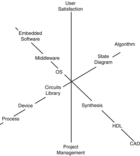
Therefore, the discipline of SoC design is intrinsically complicated and covers a variety of areas such as marketing, software, computing system and semiconductor IC design as described in Figure 1.5. SoC development requires expertise in IC technology, CAD, software, and algorithms, as well as management of extended teams and project and customer research.
Initially, the concept of SoC came from the PC bus system. By adopting the same bus architectures as those used in the PC, the processing of embedded applications was to be implemented on a single chip by assembling dedicated hard-wired logic and existing general-purpose processors. As the scale of integration and design complexity increased, the concepts of “design reuse” and “platform-based design” were born. The well-designed functional blocks could be reused in the later SoC.
communication architecture with specific characteristics – such as wide bit width, low power, higher clock frequency, and a tailored interface. The details of design reuse and platform-based SoC design are discussed in Chapter 2.
Figure 1.6 shows an example of SoC. Intel’s research chip [3] has 80 CPUs inside.
1.4 About this Book
This book describes design issues in mobile 3D graphics hardware. PC graphics hardware architecture with its shortcomings in the mobile environment is described, and several low-power techniques for mobile GPU and its real implementation are discussed.
Chapter 1 introduces the current mobile devices and mobile 3D graphics compared with desktop or arcade-type solutions. Chapter 2 discusses the general chip imple-mentation issue, such as how to design the SoC, and includes an explanation of SoC platforms. The SoC design paradigm, system architecture, and low-power SoC design are addressed in detail. Chapter 3 deals with basic 3D graphics, the fixed-function 3D graphics pipeline, the application-geometry rendering procedure, and the programmable 3D graphics pipeline. In Chapter 4 we articulate the differences between conventional and mobile 3D graphics, and introduce the principles of mobile 3D graphics and standard mobile 3D graphics APIs.
User Satisfaction
Algorithm
State Diagram
Synthesis
HDL
CAD Project
Management Embedded
Software
Middleware
OS
Circuits Library
Device
[image:19.476.131.363.65.323.2]Process
The design of 3D graphic processors is discussed in Chapters 5–7. Chapter 5 explains the hardware design techniques for mobile 3D graphics, such as low-power rasterizer, low-power texture unit, and several hardware schemes for low-power shaders. Chapter 6 covers the real chip implementation of mobile 3D graphics hardware. For academic architecture, KAIST RAMP architecture is introduced and the industrial architectures, SONY PSP and Imagination Technology SGX, are also described. Chapter 7 has a detailed explanation of the low-power rasterization unit with RTL code. In this chapter, readers can grasp the basic concept of how to design low-power 3D graphics processors. The future of mobile 3D graphics is very promising because people will carry more and more portable equipment in the future with high-performance displays. Finally, Chapter 8 looks at the future of mobile 3D graphics.
We also include appendices to introduce to chip design by verilog HDL The reader can run the verilog file to check the algorithms explained in the earlier chapters and get a taste of real 3D graphics chip design.
References
1 Tolga Capin, et, al., “The State of the Art in Mobile Graphics Research”, IEEE Computer Graphics and Applications, Vol. 28, Issue 4, 2008, pp. 74–84.
2 Gordon E. Moore, “Cramming more components onto integrated circuits”, Electronics, vol. 38, no. 8, 1965. 3 J. Held, et al, “From a Few Cores to Many: A Tera-scale Computing Research Overview,” white paper, Intel
[image:20.476.99.365.66.286.2]Corporation, www.intel.com.
2
Application Platform
2.1 SoC Design Paradigms
2.1.1 Platform and Set-based Design
2.1.1.1 Definition of a Platform
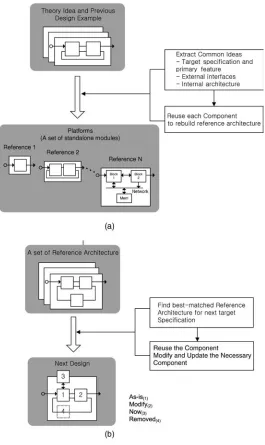
Two steps are encountered in any design process: “planning” and “making.” Certain procedures are followed when we want to perform meaningful tasks towards building a target structure. As the target structure takes on more complexity, well-established design procedures are essential. This applies in SoC design, which is strongly driven by its target applications such as multimedia and mobile communications. SoC engineers have to consider factors like quality, cost and delivery (QCD). In that sense, their design procedures naturally seek the reuse of previously developed techniques and materials at every possible design step.
In a popular English dictionary, a “system” is defined as asetand away of workingin a fixed plan with networks of components. In addition to this, SoC requires one more idea, which is the integration of components on a single semiconductor chip. So it follows that we need to focus on two concepts: the fixed plan, and integration. We can catch the concept of predetermined architecture from the fixed plan; and integration involves the network and component-based design. Considering that modern digital gadgets require not only hardware (HW) components but also software (SW) programs, we can begin to see what the “platform” means in SoC design.
The platform is a set of standalone modules that become the basis of the system. These standalone modules are pre-integrated and combine HW and SW components – we call them the “reference architectures.” They are also verified and have well-defined external interfaces. The platform guides what designers do, and this guidance determines the design flow. The platform concept helps us to design a more compli-cated and less buggy system within limited QCD factors by reusing and upgrading pre-built HW and SW components.
Mobile 3D Graphics SoC: From Algorithm to Chip Jeong-Ho Woo, Ju-Ho Sohn, Byeong-Gyu Nam and Hoi-Jun Yoo
In this part of the chapter we will discuss what the platform is and what it does. We will explain how the platform can be extracted from earlier design examples and how it can be used for a new design. The concept of modeling and its relationship with the platform will also be examined. We then go on to discuss the system architecture and software design in detail in the following sections.
2.1.1.2 Platformization
Sometimes, use of the word “platform” seems to be a little confused. Many engineers tend to think that a platform is a kind of restriction. However, we need to consider a platform in two respects: its philosophy and its management. By philosophy we mean how a platform is derived from the ideas, theory and history of pre-designed samples. It also encompasses how we can use the derived platform for new designs. By management we mean the directions the platform – and the designs guided from that platform – should be evolved and maintained. We should avoid trying to make a design tool such as a design wizard program while developing the platform. The platform is not intended to generate design examples automatically. Instead, it is better to approach the platform as a design methodology, which is a set-based design. That can lead us to the many benefits of design planning and our design procedures.
When developing a platform for a given design set and research area, we will try to analyze pre-designed examples and extract some common ideas in those designs. The ideas may include target design specifications with a primary feature set, external interfaces and internal architecture. After collecting these common ideas, we can make the basic standalone modules and define the platform by reusing the individual components and arranging them under categories and levels of primary features. This procedure resembles inductive reasoning, which derives general principles from particular facts and instances. In this process, it is very important to categorize the primary features and link them to each specification level (such as low-, middle-, or high-performance levels) when building the reference architectures. Actually, when we design something, we are first given the target specifications and primary feature set to be designed. The detailed architecture and design plan doesn’t matter for this step. We should plan to design our target based on previous examples and theory by using previous knowledge and experience. The platform is then the collection of our design history and theories. So, categorization and arrangement of primary features are the guideline to distinguish the reference architectures in the platform.
definitions of the reference design. This is the set-based design approach and resembles deductive reasoning, which generates specific facts and conclusions (our new design) from the general premises (our platform). Therefore,platformizationcan be understood as inductive and deductive reasoning, which helps us to develop a new, more complex design with very controlled and acceptable resources.
Figure 2.1 illustrates the design process. We have mentioned that the common ideas extracted from previous designs and theories contain the specification, external interface and internal architectures. In real designs, the specification and definitions of external interfaces tend to influence and decide the internal architectures to a certain extent. The definitions of internal architecture contain the following components.
Primary processing elements – What kinds of task are required and what are the related computing units?
Memory architecture – What kinds of processing result are stored for next time and how many memories are required?
Internal network – How can the processing elements and memory components be connected and interfaced with each other? And how are the internal elements connected to external interfaces?
Programmer’s model – How can software developers use the HW devices to complete the functions of the target design?
In set-based design, the reference architecture is applied as a starting point for the target design. As shown in the figure, there are four options: “As-is,” “Modified,” “New design,” and “Removed.” “As-is” means the reuse of components. Since the reference architecture is not the final design output, additions and modifications are always necessary. However, the set-based design approach can help us concentrate on the updated parts and reduce design costs.
2.1.1.3 Mobile 3D Graphics Example
The operational sequence, orpipeline, of mobile 3D graphics consists of geometry and rendering stages, which are explained in Chapter . In this subsection, the platformiza-tion of mobile 3D graphics will be briefly described as an example of the earlier discussion.
more programmability is integrated. In the software part, we have the industry-standard API, OpenGL-ES, for mobile 3D graphics [5]. It is also evolving from the application of compact and efficient architecture into integrating more programma-bility in the next version.
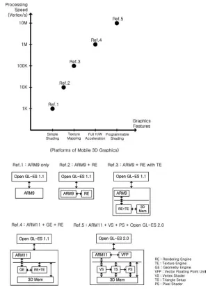
Figure 2.2 shows the range of graphics specifications and their reference archi-tectures. For people wanting high-end graphics performance, programmability and full HW acceleration are necessary. In contrast, simple shading is required by some people who just want simple graphics such as the user interface of a small cellular phone. As more graphics functions are required, the processing speed must also be increased. As the target design moves towards high-end performance, more HW accelerators and programmability will be applied. The reference architecture depicted in the figure
shows typical HW building blocks and the related software OpenGL-ES library. Some HW blocks such as a rendering engine (RE) and a texture engine (TE) are reused in two more of the reference architectures. The vertex shader (VS) and pixel shader (PS) are newly introduced in the reference architecture of the highest performance range. So, when designing a new mobile 3D graphics system including HW and SW, we can decide on the reference architecture by inspecting target specifications and graphics features. Then we can complete the design by reusing, updating and optimizing the additionally necessary SW and HW components based on the chosen reference architecture.
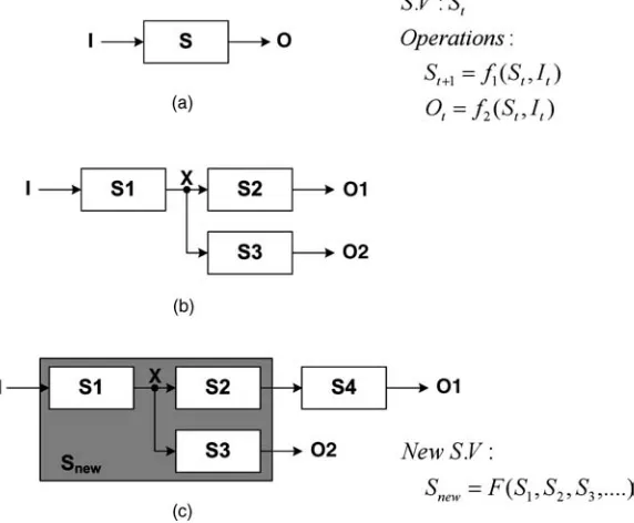
2.1.2 Modeling: Memory and Operations
2.1.2.1 Memory and Operations
How can the platform be derived from earlier design examples? Asking this question may help us to make and use the platform for our new design more efficiently.
When we design electrical components, there are certain requirements to drive signals or store information for future use. These actions are related to memory or, in other words, state variables. If an external stimulus and internal activity do not affect any part of the internal memory contents, we can say that nothing important happened. Then, after defining memories, we can consider what types of operation can be performed on them. So, we can imagine that an electrical component actually consists of the memory and the operations. In that sense, modeling can be defined as deciding on the memory architecture and its related operations for the target components. The design of an electricalsystemcan be regarded as the process that defines its memories and operations by reusing and combining sub-components that are also defined as memories and operations.
Figure 2.3 outlines the modeling and design methodology. The basic elements can be defined by their memories and operations, and the memories can be called state variables. Then we have two design methods. The first ismodular design. This means that every element can be developed independently and reused to provide multiple functions. Many interconnections – such as serial, parallel, and feedback networks – can be implemented. So, for example, one output of element A can be fed into one input of element B. The second method is hierarchical design. Here, elements can be organized as parent–child or tree-like structures to permit complex functions. The state variables are newly defined and the details of internal operations are encapsulated. This process can be repeated many times, step by step. Complicated designs are made possible by combining simpler elements.
sub-elements, and be reused by being combined and modified with other elements. We can update some parts of the reference design by changing the definitions of memories and operations. However, to maximize the efficiency of reuse in the reference design, we should restrict changes of input and output ports in the model of sub-elements as much as possible. This can be controlled because we know the influence of those changes by using modular and hierarchical design methods. Changing internal definitions of memories and operations does not result in changes in other parts of the whole design, and changing definitions of input and output ports can be clearly traced through the design hierarchy.
[image:27.476.103.389.69.305.2]platform and set-based design, can help us not only to build the design but also to analyze particular cases of using the design, because the interfaces and internal architecture are clearly defined.
Figure 2.4 shows an example. Part (a) shows the block diagram of a mobile 3D graphics system that can perform full programmable graphics pipeline operations, including a vertex shader and a pixel shader. Part (b) illustrates a case of a game application including game logic operations and graphics operations. The game logic operations – such as game physics and artificial intelligence – are performed on the ARM11 host processor with a vector floating-point unit. Then the ARM11 commits the graphics commands into the graphics sub-system. The vertex shader is invoked first. Then a triangle setup and pixel shader follows. In this figure, note that the 3D memory block is accessed many times by multiple functional units. Finally, the ARM11 reads the final graphics results from the 3D memory. This analysis can inform us that the 3D memory block should be carefully designed for best performance.
2.1.2.2 Applications of Analog and Digital Designs
The modeling and design methodology discussed in the previous subsection can be applied to both analog and digital designs. Figure 2.5 shows examples.
In both analog and digital designs, devices manufactured with silicon materials are used – so-called semiconductor materials. The behavior of these materials is explained by physics and electromagnetic theories such as wave equations and Maxwell equations. From the viewpoint of memory and operation modeling, the electronic charges and vector fields (such as electronic and magnetic fields) are the memories. The values of those parameters represent the information carried by the materials. The governing equations define the operations performed on those memories.
operational amplifiers and analog filters – by using circuit elements. The voltages at important nodes and currents in important circuit paths can now be introduced as new state variables. If we repeat the same process in steps, we can build functional blocks such as analog-to-digital converters, mixers and tuner, and finally an analog radio as the product. All these processes can be understood by the modular and hierarchical design methods.
Digital design also shows the same sequences. By using silicon materials and circuit elements, we can make logic gates such as AND, OR, and NOT. Then the logic blocks such as registers and adders can be developed. Again, the voltages at important nodes can be defined as the memories. By using logic blocks, we can build functional blocks such as an arithmetic and logic unit (ALU) and a control unit, and then finally the product such as a RISC processor can be released.
The above concepts in modeling, design methodology and platform should be kept in mind during all design processes. The use of a reference architecture and set-based design results in reduced design costs and permits the development of more advanced design targets. The modular and hierarchical approach based on memory and operation modeling can make it possible to divide complex problems and keep the focus on more easily handled sub-elements.
2.2 System Architecture
2.2.1 Reference Machine and API
2.2.1.1 Definition of Reference Machine
We have described the reference architecture as the standalone module that becomes the basis of the system, and the platform as a set of those standalone modules. Now we need to step inside the reference architecture.
When deciding to implement a real system by using the reference architecture, we have to consider which parts will be mapped into software and which into hardware. The software will run on general-purpose processing elements such as RISC processors or digital signal processors (DSPs). The hardware parts can be mapped into hardware accelerators or application-specific processors with their own instruction set, such as DirectX graphics shaders. However, before beginning the separation of HW and SW parts, we have to consider how programmers or applications engineers approach the target system efficiently. Programmers require function lists that cover all possible things they can do with the system. They do not need to know how the system works internally. On the other hand, hardware or system engineers need to know how each function is actually implemented in the system. They will also want to keep the feature set within a controlled range in order to ensure design feasibility. In relation to this we can introduce two concepts concerning the reference architecture.
Global states are the memories that can be shared between datapaths. Selectors
interconnect between datapaths. The output port of one datapath is connected to the input port of another datapath. The selector also performs operations such as multi-plexing of multiple inputs, which are controlled by some parameters.
The second concept is the application programming interface (API). It can be defined as the programmer’s interface to target the reference machine. It totally encapsulates the internal structure of the reference machine. APIs can be categorized as data processing operations, control operations and memory operations. They are related, respectively, to datapaths, selectors and state variables in the reference machine. Therefore, any application algorithm expected to use the target reference machine should be described by using only the defined APIs. Any additional functions not covered by the APIs should be implemented by using other computing elements or processors that are outside the target reference machine.
After defining the reference machine and APIs, the system architect has to decide which parts of the reference machine will be implanted as hardware and which as software, by analyzing the performance requirements (covered in a later section).
We can say that the reference architecture is composed of the implementation of the reference machine and its APIs. Of course, the APIs can be also reused between different reference architectures. The implementation level of the reference machine is decided by the target performance requirements, so we can state the following definition and simple equation:
Platform:a set of reference architecture
Reference architecture¼implementation of reference machineþAPI:
Building the reference machine and APIs in a given design problem is not an easy task, but the simplest approach is to use memory and operation modeling. After defining the memories and operations for each algorithmic description of the design problem, the system architect can merge and rearrange the primary operations modularly and
hierarchically in order to build the reference machine. In this, the definitions of local and global states are very important.
In mobile 3D graphics, there are now industry-standard APIs. OpenGL-ES is a well-defined subset of desktop OpenGL, and adopts various optimizations such as fixed-point operations and redundancy eliminations for mobile devices with low processing power. In its latest version, OpenGL-ES enables fully programmable 3D graphics such as vertex and pixel shading. Mobile 3D graphics are being improved towards even more functionality and programmability in both of hardware and software, while achieving low power consumption.
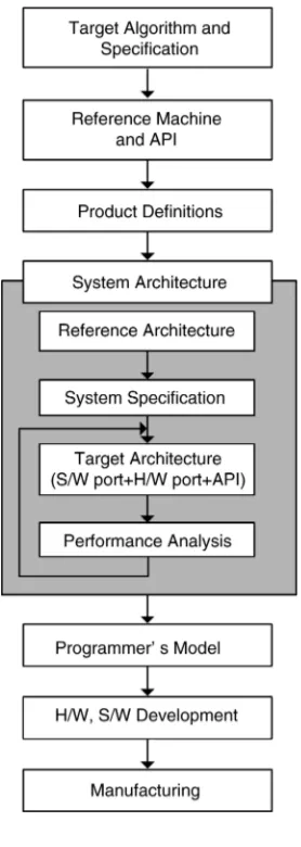
2.2.1.2 SoC Design Flow
Figure 2.7 shows the design process from target specification to manufacture, with the focus on system architecture.
The target specification defines the type of product and rough performance requirements. Suitable algorithms are chosen to meet the specification using computer programs such as a programming language, UML [6] or MATLAB.
In the system specification, the performance of the system is given but the implementation details are not determined yet. The fact that the system has to be implemented on a chip (SoC) means that the software running on the embedded CPUs should be designed concurrently. This is the big difference between SoC design and VLSI (very large scale integrated) design. Determination of which parts of the specification will be implemented in hardware and which in software is included in the design process.
Once the concept of the target system has been grasped, the set of functions to realize the system specification should be derived and divided into more affordable unit functions. Therefore, the functional specification of a system is determined as a set of functions which calculate outputs from the inputs.
As mentioned in the previous subsection, the reference machine and its APIs can be developed from the algorithm descriptions by using memory and operation modeling. Then, we go into the step of product definition. This involves the naming of the product, “is/is-not” analysis, priority analysis, and competitive analysis. “Is/is-not” analysis is the process of defining the desired level of development: unnecessary features should be identified in order to prevent wasting design resources. Priority analysis includes the schedule, costs, and power consumption. Because the development process is always controlled by a limited delivery time, some parts of the first design plan might have to be abandoned.
the set-based design approach. Then, documentation of the system specification can be prepared.
The system specification can contain the following items:
1. Summary of product requirements 2. List of features
3. Top-level block diagram 4. Use case descriptions
[image:33.476.176.315.63.453.2]5. Availability and status of functional blocks (As-is, New, Modified, Removed) 6. Block specification
7. Integration and communication specification 8. Power specification
9. External interface (Pin list, Pin multiplexing, Package) specification.
Although the initial specifications and performance requests are a little indistinct, the system specification describes the target product more concretely. By using the system specification and reference architecture, we can decide the internal architecture of software and hardware parts in more detail. Having decided the target architecture, we can estimate factors such as silicon area, power consumption, processing speed and memory requirements. For each use case, the performance analysis is performed to reveal bottlenecks and wastage of resources. If the performance does not meet the requirements, the target architecture should be modified. So the target architecture and performance analysis will be repeated until the performance meets the target requirements.
When the system architecture is finalized, the programmer’s model for the target product should be defined. The APIs are a kind of top-level software interface. To realize each API function, there should be invocations of some hardware blocks or processing elements that have their own internal architectures. Therefore, we need descriptions of how the API developers can use each functional block in the target architecture. The programmer’s model defines the behavior of each functional block. The following items can be identified:
1. Memory map and instruction sets 2. Memory format and memory interface 3. Register set
4. Exception, interrupts and reset behavior 5. External interface and debug interface 6. Timing and pipeline architecture.
At this stage we have all the descriptions of internal architecture in both the software and hardware parts. The remaining steps are SW/HW development and manufacture. Common semiconductor design processes such as register transfer level (RTL) descriptions with synthesis and custom design with circuit simulations can be employed.
2.2.2 Communication Architecture Design
2.2.2.1 Data and Command Transfers
a system is producing something that is immediately consumed by another component of the system. In fact, this features multimedia signal processing itself.
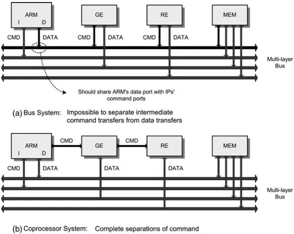
Going deeper into the real implementation, there are two kinds of information transfer:command transferanddata transfer(Figure 2.8). Command transfer uses information to control operations of building blocks such as register settings or small program codes. Mostly, command transfer is not shown in the diagram of a reference machine; it appears clearly after the step of system architecture is finished. Data transfer uses information to give intermediate results from the current processing block to the next processing block. As explained in the definition of the reference machine, there are transfers of local states and global states in these data transfers. In general, the bandwidth of data transfer is higher than for command transfer.
2.2.2.2 On-chip Interconnections
The demand for high performance of semiconductor devices has required increased operating frequency of the silicon chip. However, owing to the difficulty of imple-mentations such as clock distributions, the design approach of SoC with multiple functional units has been widely adopted in multimedia and communication applica-tions. As mentioned earlier, on-chip interconnections between the functional units influence the whole system performance in SoC design.
Generally, the host processor in the SoC has its own instruction set and memory space. Therefore, in the programmer’s model, the functional unit can be attached in the memory space or in the instruction set. In a real implementation, the former adopts on-chip bus architecture and the latter adopts coprocessor architecture. The on-on-chip bus provides shared data wires that can be connected with data ports of multiple functional units. These data wires can be unidirectional or bidirectional. Each address port of the functional units is decoded and arbitrated by bus arbiters in the on-chip bus architec-ture. If the programmer accesses the address space mapped to some functional units, the bus arbiters enable the related functional unit to access the shared data bus while keeping other functional units from interrupting the data transactions. There can be
multiple layers and multiple arbiters in the on-chip bus architecture for increased performance.
In the modern embedded RISC processor, the coprocessor is defined as a general mechanism for extension of the instruction set architecture. The coprocessors have their own private register set and state, and these are controlled by coprocessor instructions that mirror the host processor instructions controlling the host processor’s register set. The host processor has sole responsibility for flow control, so the coprocessor instructions are concerned only with data processing and data movement. Following RISC load–store architectural principles, these categories are cleanly separated.
[image:36.476.87.376.348.578.2]Figure 2.9 compares the on-chip bus and coprocessor architecture in terms of data and command transfers. Conventional bus architecture implies that an additional hardware block attached in the memory space should be connected with the data port of the main processor. This is because a modern embedded RISC processor does not have a dedicated port for memory-mapped components. Therefore, the command transfers of hardware blocks use the bus shared with main memory transactions, causing inefficient utilization of processing elements. In addition, multi-layer bus architecture requires complex interconnections including multi-port arbiters with long and wide global metal wires, leading to high power consumption. Also, concentrated data transactions may cause heavy bus arbitrations, and the main processor should always consider thread synchronizations in invoking bus-attached
hardware blocks. On the other hand, the coprocessor system shows the following features.
a. A direct signal path with short coprocessor interfaces provides simple interconnec-tions. Coprocessors share a bypassed instruction port with the main processor. They do not need bus arbitrations for hardware access, unlike conventional bus-attached hardware accelerators. Therefore, the coprocessor interface can reduce unwanted delays between the main processor and hardware accelerators, and thus relevant power consumption.
b. Since the coprocessor operates in locked step with the core pipeline of the main processor, complex synchronization is avoided.
c. Since the commands of the coprocessor are regarded as extended instruction set architectures of the main processor, easy programmability can be achieved.
However, the interface coprocessor architecture is strongly dependent on the architecture of the host processor while the on-chip bus uses a typical memory interface. Therefore, the coprocessor cannot fully achieve the reusability of platform and set-based design. Which on-chip interconnections should be used will be deter-mined by the performance requirements and availability of other functional blocks. Recently, a new on-chip interconnection scheme has been introduced in SoC design. The network-on-a-chip (NOC) uses computer network concepts in its on-chip inter-connections [7]. Instead of a circuit-switched network of conventional bus architec-ture, packet data transfers and fast low-voltage serializations achieve high data bandwidth while keeping the power consumption low.
2.2.3 System Analysis
One of the most important tasks of a system architect is the analysis of system performance during the development of system specifications. Generally the items to be estimated are memory bandwidth, memory capacity, processing speed, power consumption, and silicon die area.
The memory capacity and memory bandwidth can be analyzed by checking defined use cases. According to the definitions of memory mapping and the formats of memory contents such as addressing schemes, the required memory bandwidth and memory capacity can be varied. Careful assignment of memory space is very important. Use case analysis can clarify which memory accesses should be done separately. Because dynamic random access memory (DRAM) is widely used, the estimation margin should be addressed to compensate for read and write latencies. The total required memory bandwidth should be restricted to less than 60% of peak DRAM bandwidth in most cases.
as parameters for power estimations. Voltage scaling and other technology advantages can be also considered. The active power of processing can then be computed by summing the power consumptions of all functional units. If the power consumptions are known in terms of mW per MHz, the operating frequency will determine the actual power consumption, and the operating frequency is determined by use case analysis taking into account processing loads in the functional units. The leakage power can be computed by estimation of the equivalent number of basic logic elements such as 2-input NAND gates for a given functional unit. Many semiconductor manufacturers provide the leakage power consumption of these basic logic gates under various operationing conditions, such as voltage and temperature. We can make use of the following relations in power estimations:
Total power consumption ¼active powerþleakage power
Active power of RISC sub-system ¼constant powerþ(core factor(mA/MHz)þ memory factor(mA/MHz)þperipheral factor(mA/MHz))*voltage*frequency
Active power of HW accelerators ¼ gate power factor(mA/MHz/gate)*gate count*activity level*voltage*frequency
Leakage power ¼logic leakage powerþmemory leakage power
Logic leakage power ¼2-input NAND leakage power*gate count
Memory leakage power ¼ bit-cell leakage power*capacityþ2-input NAND leakage power*memory array logic factor*capacity
Estimation of the silicon die area is important because it influences the selling price of the silicon chip. Although there is likely to be some overhead to account for internal interconnections, summation of the silicon areas of the functional units can provide meaningful information before real implementations. Of course, the shrink-down effect of semiconductor technology advances should be considered when using parameters from earlier designs. Many semiconductor manufactureres also provide the routing efficiency and integration density in terms of the number of transistors per unit area. The following simple equations can be used in die area estimations:
Logic area ¼gate count*gate density
Memory area ¼equivalent gate count*gate density or memory macro area
Sub-modulelogic area ¼sum of building block logic area*(1þPnR fix-cell over-head)*(1þclock tree overhead)*(1þhold-time fix overhead)*(1þlarge buffer overhead)
Sub-module macro ¼sum of macro block area*(1þmacro overhead)
Sub-module total area ¼sub-module logic areaþsub-module macro area
Top core area ¼ sum of total logic areaþsum of total macro area*(1þmacro placement overhead)
2.3 Low-power SoC Design
Low-power design methodologies are well developed and are actively employed in the design of SoC for cellphones [8–11]. Low power operation can be obtained at each design level. This section briefly introduces the principles.
2.3.1 CMOS Circuit-level Low-power Design
CMOS logic devices consume power when they are operating. There are two major elements to active power dissipation: dynamic switching power and short circuit power. A third element is the leakage power that results from sub-threshold current, or the current flowing through a MOSFET whenVgs¼0 V. The total power is given by the following equation:
Ptotal¼PswitchingþPshort-circuitþPleakage ¼a0!1CLVdd2 fCLKþIscVddþIleakageVdd:
Low-power design methods aim to decrease power dissipation by reducing the values ofa0!1,CL,Vdd2, andfCLK. Various techniques and their effects on the terms of the power equation are summarized in Table 2.1. The node transition activity factor is a function of the Boolean logic function being implemented, the logic style, the circuit topologies, signal statistics, signal correlations, and the sequence of operations. However, most of the factors affecting the transition activity are determined by the logic synthesis EDA tools.
2.3.2 Architecture-level Low-power Design
There are many low-power schemes above the level of register transfer level designs. The most common method is clock gating, which disables unnecessary blocks in the synchronous system. The clock is connected to the internal circuits through an AND gate which is controlled by the gate enabling signal. This scheme can be applied block by block to selectively control the power consumption.
At the architecture level,parallelismcan be used to reduce power consumption. For example, if one puts an identical functional module in parallel with the original one, Table 2.1 Summary of low-power techniques for SoC
Toggle count Logic style; transition reduction coding Load capacitance Wire length minimization; partial activation Voltage scaling (VS) Small swing
MultiVdd; dynamic VS; adaptive VS
MultiVth; variableVth(substrate bias); negativeVgs
one can double the throughput of the functional operation, and the clock frequency can be halved if the throughput is the same as for the original one. Pre-computation can remove unnecessarytogglestoo. Before the main operation of the circuit, a part of the circuit is pre-computed and the internal switching activities of the main circuit are controlled by using the pre-computed results to reduce the number of toggles.
2.3.3 System-level Low-power Design
A SoC or subsystem has one or more major functional modes, prime examples being operational mode, idle mode, sleep mode, and power-down mode. The operational mode is when the SoC operates its normal functions. In the idle mode, the clock block is ON but no signal is switching. In the sleep mode, even the clock part is OFF as well as the main blocks. When the SoC is turned off with the power supply connected, the SoC is in power-down mode. At the system level, low-power solutions are “multi-supply voltage” or “voltage scaling,” “power shut-off,” “adaptive voltage scaling,” and “dynamic voltage and frequency scaling.”
In system-level low-power schemes, the SoC is divided into multiple voltage and frequency domains, and then it adopts DVFS (dynamic voltage–frequency scaling), AVS (adaptive voltage scaling), andpower shut-off orpower gating to control the power dissipation in each domain.
2.4 Network-on-Chip based SoC
As chip integration evolves, current SoC designs incorporate a number of processing elements to meet performance requirements with reasonable power consump-tion [1–3]. This design trend makes it simpler to achieve high performance with moderate design effort because a verified processor core can be replicated. In addition, SoC design requires integration of numerous peripheral modules such as on-chip memory, an external memory controller, and I/O interfaces. As a result it is very important to provide efficient interconnections between numerous processing cores and peripheral modules within an SoC.
Traditional bus-based interconnection techniques are not suitable for current large-scale SoCs because of their inherent poor scalability, so a design paradigm based on network-on-a-chip (NoC) has been proposed as a solution for on-chip interconnection of large-scale SoCs [4, 5]. The modular structure of NoCs makes chip architecture highly scalable, and well-controlled electrical parameters of the modular block improve reliability and operation frequency.
2.4.1 Network-on-Chip Basics
2.4.1.1 Homogeneous and Heterogeneous SoCs
Network-on-chip architectures are emerging as a strong candidate for a highly scalable, reliable, and modular on-chip communication infrastructure platform for high-performance SoCs [12, 13].
To date, there have been two distinct types of SoC: homogeneous and heteroge-neous. WithhomogeneousSoCs, suitably designed modules are replicated and placed on a single chip in a regular topology. MIT’s RAW processor [16] and Intel’s 80-tile processor implementation [11] are examples with two-dimensional mesh topology. These processors consist of modular tiles that include a processing core and 5-port crossbar switch. In each tile, the 5-port crossbar switch provides connections to the four neighboring tiles of a mesh topology and processing core inside the tile. For homogeneous SoCs, crossbar switches are commonly adopted instead of the conven-tional bus, because the non-blocking characteristic of the crossbar switch has the advantage of enabling concurrent interconnections among multiple processing cores and peripheral modules. Figure 2.10a depicts how the homogeneous SoC is organized in a regular array structure.
AheterogeneousSoC [17, 18] integrates various functional modules that are usually dedicated to accelerating specialized computations of the target application. With a heterogeneous SoC it is difficult to build up regular structures – such as a two-dimensional array of processors – because the sizes of the functional modules are different from each other. In addition, adopting regular interconnections may result in waste of wire resources owing to highly localized and fixed traffic patterns among functional modules. Therefore, in most cases, a heterogeneous SoC requires optimized
interconnections that are tailored to the data traffic patterns of the target application. Figure 2.10b shows a simplified example.
Entirely homogeneous or heterogeneous SoCs have been introduced above to highlight the distinctions between the two types, but hybrid versions will be in widespread use in the near future. The homogeneous architecture is mainly beneficial for providing huge computing power, so integrating additional functional modules such as external I/O or application-specific accelerators is usually necessary, and this results in the need for a hybrid architecture. Then, scalablity and structured interconnections are essential to establish efficient interconnections for a complex SoC architecture. When compared to the conventional bus and point-to-point architecture, NoC has huge advantages. The next subsection expands on the benefits of adopting NoC.
2.4.1.2 Comparison of NoC and Buses
NoC-based SoC design uses two major concepts that are distinguishable from those of bus-based SoC architecture. There are packet transactions rather than circuit transac-tions, and there is a distributed network structure instead of a conventional globally shared bus or a centralized matrix. In NoC-based SoC design, each of the functional modules should be designed to be latency-insensitive, to support packet transactions. Although this makes functional module design slightly more complex, many benefits are gained from having packet transactions. It improves reliability and the speed of interconnection links, because packet transactions are intrinsically pipelined so that the physical lengths of interconnection links can be kept short. Efficient link utilization is another advantage, because only part of the end-to-end path between functional modules is occupied by the traversing packets. It is also advantageous that the electrical parameters of one NoC are not influenced by the addition of other NoC modules, owing to the structured characteristic of the NoC. This enables the building up of large-scale SoCs from smaller existing components by the addition of any required functional modules. For all these reasons, advanced bus architectures, too, are gradually considering a packet transaction concept into their protocols; examples are multiple-outstanding addressing, split transactions, and multi-threaded transac-tions [19, 20]. In the near future, it is expected that commercial bus architectures for a high-end SoC will take the NoC design into their specifications [21, 22].
several layers that are independent of each other, so that the design procedure becomes more manageable and easily modifiable. The detailed correspondence of NoC to the OSI reference model will be described in a later subsection.
First we will briefly summarize the pros and cons of NoC-based design and bus-based design as shown in Table 2.2. For many reasons, NoC-bus-based design is advantageous; the details are addressed in the table.
2.4.1.3 NoC Design Issues
Figure 2.11 illustrates the overall architecture of an NoC. First, an appropriate topology and protocol should be selected when NoC design begins. The NoC topology can be configured with regular topologies such as “mesh,” “torus,” “tree,” or “star.” Alternatively, an optimization can be carried out to build an application-specific topology without a regular pattern. Second, protocols including packet format, end-to-end services, and flow control should be defined and implemented in a network interface (NI) module. Packet size definition affects the buffer capacity requirement and multiplexing gain in the network.
The packet switching scheme is the next factor to be determined. There are many switching methods such as store-and-forward, wormhole switching, and cut-through switching.
. Store-and-forward. The entire data of a packet at the incoming link are stored in the buffer for switching and forwarding. A buffer with a large capacity is required.
. Wormhole routing. An incoming packet is forwarded right after the packet header is identified and the complete packet follows the header without any discontinuity. The path that the packet occupies traveling through the switch is blocked against access by other packets.
. Virtual cut-through. The path is determined as with wormhole routing. If the next hop is occupied by another packet, the packet tail is stored in a local buffer to await clearing of the path. Its buffer size can be smaller than the store-and-forward switch; but if the packet size is large, many local buffers are occupied to delay the switch throughput.
Choosing an appropriate switching scheme to suit the target application and silicon resource budget is necessary. In many NoC implementations a wormhole routing scheme is chosen because of its lower buffer resource requirement.
Network-on-chip Bus
Bandwidth and speed .Nonblocked switching guarantees multiple concurrent transactions.
þ
.Pipelined links: higher throughput and clock speed.
.A transaction blocks the other transactions in a shared bus.
.Regular repetition of similar wire segments which are easier to model as DSM interconnects.
.Every unit attached adds parasitic capacitance; therefore electrical performance degrades with growth.a[24]
Resource utilization .Packet transactions share the link resources in a statistically multiplexing manner.
þ .A single master occupies a shared bus during its transaction.
Reliability .Link-level and packet-basis error control enables earlier detection and gives less penalty.
þ .End-to-end error control imposes more penalty.
.Shorter switch-to-switch links, more error-reliable signaling.
.Longer bus wires are prone to errors.
.Rerouting is possible when a fault path exists. (self-repairing).
.A fault path in a bus is a system failure.
Arbitration .Distributed arbiters are smaller, thus faster. þ .All masters request to a single arbiter; thus the arbiter becomes big and slow, which degrades bus speed.
.Distributed arbiters use only local information, not a global traffic
condition
þ .Central arbitration may make a better decision.
Transaction energy .Point-to-point connection consumes the minimum energy.
þ .A broadcast transaction needs more energy.
Modularity and complexity
.A switch/link design is re-instantiated, thus less design time.
þ .A bus design is specific, thus not reusable.
.Decoupling between communicational and computational designs
Scalability .Aggregated bandwidth is scaled with network size.
þ .A shared bus becomes slower as the design bigger, thus it is less scalable.
Mobile
3D
Graphics
[image:44.476.88.638.64.409.2]fashion don’t need a globally synchronized clock: very advantageous for high-speed clocking.
whole chip bus area.
Latency .Internal network contention cause a packet latency.
þ .Bus latency is wire-speed once a master has a grant from an arbiter.
.Repeated arbitration on each switch may cause cumulative latency.
.Packetizing, synchronizing, interfacing cause an additional latency.
Overhead .Additional routers/switches and buffers consume area and power.
þ .Less area is consumed.b
.Fewer buffers are used.b Standardization .There is no NoC-oriented global standard
protocol yet; however, legacy interfaces such as OCP and AXI can be used.
þ .AMBA and OCP protocols are widely used and designed for many functional IPs.
a
Recent advanced buses are using pipelined wires by inserting registers in between long wires [14, 15]. b
Recent advanced buses use crossbar switches and buffers (register slices) in their bus structure.
Platform
ports. When conflicts occur, the scheduler should resolve them according to a pre-defined algorithm. Buffers are important to store the packet data temporarily for congestion control.
There are three queuing schemes distinguished by the location of the buffers inside the router (switch): input queuing, output queuing, and virtual output queuing (Figure 2.12).
. Input queuing. Every incoming link has a single input queue so thatNqueues are necessary for an NN Switch. Input queuing suffers from the “head-of-line” blocking problem; that is, the switch utilization is saturated at the 58.6% load.
. Output queuing. The queues are placed at the output port of the link, butNoutput queues for every outgoing link are required to resolve the output conflict, resulting in
N2queues. Owing to the excessive number of buffers and its complex wiring, in spite of its optimal performance, output queuing is not used.
. Virtual output queuing. The advantages of input queuing and output queuing are combined. A separate input queue is placed at each input port for each output, requiringN2buffers. The “head-of-line” blocking problem is resolved by scheduling. Complicated scheduling algorithms such as iterative algorithms are needed. Figure 2.12 Queuing schemes: (a) input queuing, (b) output queuing, and (c) virtual output queuing
The last issue in Figure 2.12 is flow control or congestion control. There are several solutions which prevent packets from output conflict and buffer overflow.
. Packet discarding. Once the buffer is overflowed, the packets coming next are simply dropped off.
. Credit-based flow control. A back-pressure scheme uses separate wires for the receiver, to notify congestion of the buffer to the transmitter to prevent packet loss, as shown in Figure 2.13a. The propagation delay time between transmitter and receiver should be considered carefully to avoid packet transmission while the wait signal is coming on the wire. In theWindowscheme of Figure 2.13b, the receiver regularly informs the transmitter about the available buffer space.
. Rate-based flow control. The sender gradually adjusts the packet transmission according to the control flow messages from the receiver. For example, the error control uses Go-back-Nalgorithm and related signals. In this case, a certain amount of buffer space is guaranteed for effective flow control, but owing to its long control loop, rate-based flow control potentially suffers from instability.
In addition to the basic design parameters required to be determined for an NoC design, additional functionalities are required to enhance NoC performance and optimize the cost overhead. Quality of service is one of the most critical issues. The quality factors in an NoC should be bandwidth and latency. Guaranteed bandwidth and limited latency enable packet transactions to be punctual, thus making it possible to execute real-time applications in the NoC-based SoC.
2.4.1.4 NoC Building Blocks
The circuits of the basic building blocks will be introduced. The basic building blocks are high-speed signaling circuits, queuing buffers and memories, switches, crossbar switch schedulers, and SERDES.