I
I
LCD-2 SERIES&LAMBDA
INSTRUCTION MANUAL
FOR
REGULATED POWER SUPPLIES
LCD-2 SERIES
This manual provides instructions intended for the operation of Lambda power supplies, and is not to be reproduced without the written consent of Lambda
Electronics Corp. All information contained herein applies to alLLCD-2 models
unless otherwise specified.
TABLE OF CONTENTS
Section
SPECIFICATIONS AND FEATURES
THEORY OF OPERATION
OPERATING INSTRUCTIONS
Basic Mode of Operation
Connections for Operation
Supply-Load Connections
Operation After Protective Device Shutdown
MAINTENANCE
General
Trouble Analysis
Checking Transistors and Capacitors
Printed Circuit Board Maintenance Techniques Trouble Chart
Performance Checks
SERVICE
PARTS ORDERING
Page
1
4
6
6
6
6
8
9
9
9
9
lD
10
12
13
13
SPECIFICATIONS AND FEATURES
Specifications apply for all models.
DC OUTPUT--Voltage regulated for line and load
VOLTAGE RANGE
Model (EACH SIDE)
LCD-2-11 0-7 VDC
0-7 VDC
LCD-2-12 0-18 VDC
0-7 VDC
L:GD-2-13 0-32 VDC
0-7 VDC
LCD-2-22 0-18 VDC
0-18 VDC
LCD-2-23 0-32 VDC
0-18 VDC
LCD-2-33 0-32 VDC
0-32 VDC
LCD-2-44 0-60 VDC
0-60 VDC
LCD-2-55 0-120 VDC
0-120 VDC
TABLE I
VOLTAGE AND CURRENT RANGES
MAXIMUM CURRENT (MA) AMBIENT TEMPERATURE
40°C 50°C 60°C
300 ma 240 ma 175 ma
300 ma 240 ma 175 ma
160 ma 130 ma 100 ma
300 ma 240 ma 175 ma
120 ma 95 rna 70 rna
300 ma 240 ma 175 ma
160 rna 130 ma 100 ma
160 ma 130 ma 100 ma
120 ma 95 ma 70 ma
160 ma 130 ma 100 ma
120 rna 95 ma 70 rna
120 ma 95 ma 70 rna
65 ma 52 ma 37 rna
65 ma 52 ma 37 rna
30 ma 30 rna 22 ma
30 rna 30 rna 22 rna
AT
71 °c
115 ma 115 ma
65 ma 115 ma
45 ma 115 ma
65 ma 65 ma
45 ma 65 ma
45 ma 45 ma
23 ma 23 ma
14 ma 14 ma
Current range rnust be chosen to suit the appropriate maximum
ambient temperature. Current ratings apply for entire
voltage range.
REGULATED VOLTAGE OUTPUT
Regulation (line) ••••••• 0.01 percent plus 1.0 rnillivolt for input variations frorn 105-132 or 132-105 volts AC
Regulation (load) ••••••• 0.01 percent plus 1.0 millivolt for
load variations frorn no load to full
[image:4.615.90.468.164.550.2]Remote Programming
External Resistor Nominal 1000 ohms/ volt output
Programming Voltage ....•... One-to-one voltage change
Ripple and Noise ...•.••.•..•••... 250 microvolts rms; 1 millivolt peak to peak with 57-63 Hz input
Temperature Coefficient ...•... Output change in voltage 0.01%
+
0.3 mv/oC using an externalpro-gramming resistor, less than 0.015%
+
0.3 mv/oC with internal resi~torRemote Sensing ..•••.•..•..••... Provision is made for remote sensing to eliminate effect of power output lead resistance DC regulation.
AC INPUT-- 105-132 or 205-265 ("V" option) volts AC at 47-440 Hz. Maximum
input power*: 20 Watts. Ratings apply for 57-440 Hz.; at
47-57 Hz input derate ~urrent 10% for each ambient temperature
given in table 1.
i~ith output loaded to full 40°C rating and input voltage 132 volts AC, 60 Hz
OVERLOAD PROTECTION
Thermal ••..•.•••.•••.••••••.•.••. Thermostat, resets automatically when' over temperature condition is eliminated Electrical
External Automatic electronic current limiting
circuit, limits output current to a pre-set value less than 140% of 40°C current
rating. Automatic current limiting
protects the load and power supply when external overloads and direct shorts occur.
Internal ..••... Fuse Fl provides protection against in-ternal circuit failure in conjunction with overvoltage protector option
INPUT AND OUTPUT CONNECTIONS-~Terminal block on rear of chassis.
OPERATING AMBIENT TEMPERATURE RANGE AND DUTY CYCLE--Continuous duty from -20°C to 71°C ambient with corresponding load current ,ratings for all mode. of operation
STORAGE TEMPERATURE-(non-operating)
CONTROLS
PHYSICAL DATA
Size .•....••.••••••...•..•••..••..• 3-9/32" X 3-5/32" X 3-5/16"
Weight 2-1/4 lbs. net; 3-1/8 lbs. shipping wt.
Finish Grey, FED STD 595 No. 26081
MOUNTING - Four surfaces, each with tapped mounting holes, can be utilized for mounting this unit. Refer to figure 13 for mounting details.
"v"
OPTION - Standard LCD-2 power supplies can be obtained for 205-265 VAC,47-.440 Hz input. With 47-57 Hz input derate current 10% for each
ambient temperature given in table 1.
ACCESSORIES
Rack Adapter Rack adapter LRA-8 with or without
chassis slides is available.
Overvoltage Protector ... Externally mounted, Overvoltage Protectors LC-OV-lO, LC-OV-ll and LC-OV-12 are available for
use with Lambda LCD-2 power supplies.
Control Panel . . . ... All LCD-2 power supplies may be
obtained with a Systems Power Control
Panel, SP-3. This unit, mounted on
rack adapter LRA-8 and used with a Standard Cable or Auxiliary Cable, provides an on-off switch, voltage
control and pilot light. A single
SP-3 controls both master (M) and slave (S) unit of the power supply.
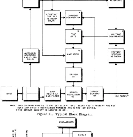
THEORY OF OPERATION
GENERAL
The text in this section refers to circuit designations for the
''M''
unit of the LCD-2 power supply, however the'discussion is equally Jipplicable
to the
"S"
unit which has electrically identical components in the 100series. except for CRl12, which is used in the
"S"
unit only.The Lambda power supply consists of an AC input circuit and transformer; a bias supply consisting of an auxiliary rectifier and filter, and
pre-regulator*; a main regulator circuit consisting of the main rectifier and filter, a series regulator, emitter follower driver, a current comparator*, a voltage comparator*, an amplifier*, current and voltage sensing networks and a voltage reference circuit*.
'/'T,hiscircuit element is part of integrated circuit (ICl) in the supply.,
The circuit arrangement is shown in block diagram form, Figure 11. The circuitry is discussed with reference to the block diagram and the schematic diagram.
FUNCTIONAL DESCRIPTION
Single phase input power is applied to transformer TI through the input circuit which contains a thermostat to protect the supply against
over-heating. Transformer TI supplies secondary power for both ''M'' and
"S"
units.The main rectifier, a full wave bridge rectifier, provides the power which is filtered by capacitor C6 and then regulated via a series regulator
and delivered to the output. Half-wave auxiliary rectifier CRI provides voltage filtered by capacitor CI for the preregulator located "in ICI. The
reference element, powered by the preregulator, provides a reference voltage for the current comparator and the voltage comparator.
Constant voltage circuit operation is determined by changes in the load
which cause a change in one input to the voltage comparator. A second input
to the comparator is a reference voltage that is developed by a constant
current 'of ,.1 milliampere flowing in divider element R8. The comparator
compares the output voltage change with the refer.nce voltage resulting in an error signal at the output of the comparator.
In constant .voltage operation the ~oltage across R7 is less than the
pre-set voltage across R6, causing the current comparator to be at cut off,. If
the load current decreases, causing a rise in output voltage, the voltage 'comparator, conducts less and more current flows through the OR :gate. This
Current limit circuit operation is determined by changes in the load. The current comparator samples load current through current sensing
re-sistor R7. When the voltage drop across· R.7 increases to the
preset voltage reference determined by R6 and R9, the current comparator
conducts. Thus, when the output current rating of the unit is exceeded,
the current comparator conducts, decreasing the current through driver Ql, resulting in an increase of voltage across the series regulator and a decrease of the output voltage, effectively limiting the output current to
a safe value. The current limit value is determined by fixed resistors
OPERATING INSTRUCTIONS
BASIC MODE OF OPERATION
This power supply operates as a constant voltage source provided the load
current does not exceed the rated value at 40°C. For continuous operation,
load current must not exceed the rating for each ambient temperature and will remain limited to less than 140% of 40°C .rating.
CONNECTIONS FOR OPERATION
NOTE: Make all connections to the unit before applying AC
input power.
Ground Connections. The Lambda power supply can be operated either with
negative or positive output terminal grounded. Both positive and negative
ground connections are shown in the diagrams for all suggested output con-nections illustrated in this manual.
Connection Terminals. Make all connections to the supply at the terminal
blocks on the rear of the supply. Apply input power to terminals 1 and 2;
always connect the ungrounded (hot) lead to terminal 1.
The supply positive terminal is brought out to terminals 6 (M unit) and 14
(S unit). The supply negative terminal is brought out to terminals 4 (M'uilit)
and 12 (S unit). Recommended wiring of the power supply to the load and
selection of wiring is shown in figures 1 through 10. Selection of proper
w~r~ng is made on the basis of load requirements. Make all performance checks
and measurements of current or voltage at the rear output terminals. Connect
measuring devices directly to terminals or use the shortest leads possible.
SUPPLY LOAD CONNECTIONS
Connections For Operation as a Constant Voltage Source
The output impedance and regulation of the power supply at the load may change when using the supply as a constant voltage source and connecting
leads of practical length are used. To minimize the effect of the output
leads on these characteristics, remote sensing is used. Recommended types of
supply-load connections with local or remote sensing are described in the following paragraphs.
Refer to figure 1 to determine voltage drop for particular cable length,
wire size and current conditions. Lead lengths must be measured from supply
terminals to load terminals as shown in figure 2.
Two-Wire Connection, Figure 3. The two-wire connection, with looal sensing,
is the connection suitable for applications with relatively constant load.
Four-Wire Connection, Figure 4. The four-wire connection with remote sensing,
Progranuned Voltage Connections, Using External Resistor, Figure 5. Discrete voltage steps can be programked with a resistance voltage divider valued at 1000 ohms/volt and a shorting-type switch as shown in figure 5. When con-tinuous voltage variations are required, use a variable resistor .with the same 1000 ohms/volt ratio in place of the resistive voltage divider and
shorting-type switch. Use a low temperature coefficient resistor to assure most stable
operation.,
As shown in figure 5, voltages can be programmed utilizing either local or remote sensing connections, as desired.
Progranuned Voltage Connections Using Programming Voltage, Figure 6. The power
supply voltage output can be programmed with an externally connected programming
power supply. The output voltage of the programmed supply will maintain a
one-to-one ratio with the voltage of the progranuning supply.
The progranuning supply must have a reverse current capability of 1.5 mao minimum.
Alternatively, when supplies with less than 1.5 ma reverse current capa-bility are used, a resistor capable of drawing 1.5 mao at the minimum progranuning
voltage must be connected across the output terminals of the supply. This
programming supply must be rated to handle all excess resistor current at the maximum programming voltage.
Connections For Series Operati~n
~he voltage capability of LCD-2 power supplies can. be extended by series
operation. A maximum of 250 volts can be connected between either the +DC
or -DC terminal and chassis ground, with a ma.ximum voltage capability of
240 volts possible for model LCD-2-55. I f a common' load is'used, the
maxi-mum current rating of the unit with the lower current rating must not be exceeded.
Figure 7 shows connections for either local or remote sensing in a series
connection where the voltage control of each unit functions independently to
control the output, and where the S unit does not track the M unit.
Units M and S are shown connected for alJto ... series operation. in fig"",re 8
and 9: Figure 8 shows the serieE? connection diagram which woq1d be suitable
for use in most applications where tracking is desired. Using externally
connected me~ers, first set the S unit output voltage adjust cont:rol for ~ero
output, then set M unit_output voltage adjust control for desired output 'voltage.
Readjust ~unit output voltage to agree with the output voltage of, the M unit.
The ~ unit will track anY change in M unit output voltage .. made with the M unit
voltage adjust control •.
Voltage divider ~ must be used during auto-series operation.
of RM according to the desired output voltage of the supply* may be applying the following formula:
E
out =where Eout is the desired supply output voltage and Idiv is the divider
current. Idiv may vary between a minimum and maximum value of one and two
milliamperes respectively.
*
On hybrid power supplies (LCD-2-12, -13, -23) desired master outputvoltage must never exceed the slave maximum output voltage rating.
Figure 9 shows the series connection diagram suitable for applications where more precise voltage tracking due to temperature changes is required.
Resistor RBAL should be a one-watt, 1 - 2 kilohm resistor. This value would permit wide-range compensation for manufacturing differences inherent in the components used in each unit. Resistors RS and RM function in the voltage sensing circuits of both units, enabling the S unit to reference
its output voltage to that of the M unit. Select RM and RS on the basis of
500 ohm to 1000 ohm per volt of M unit output voltage. RM must equal RS.
Capacitor C, used to eliminate stray AC pickup, is rated at 2.5 mf,
200V for models LCD-2-ll thru LCD-2":'44. On model LCD-2-55, C is rated at
1.4 mf 400V.
Connections For Parallel Operation
The current capability of LCD-2 power supplies can be extended by parallel operation of LCD-2 power supplies of equal* voltage capacities. Units "M" and
"s"
are shown connected for parallel operation in figure 10. One power supply designated the "master" or M unit controls its own output as well as the out-put of the second power supply, designated the "slave" or S unit.*
For applications using supplies of unequal voltage ratings, consultfactory for details of operation.
Unit S operates to regulate its current in a ratio to that of the M unit by comparing the current in its internal sampling resistor with that current sampled by the master internal sampling resistor.
OPERATION AFTER PROTECTIVE DEVICE SHUTDOWN
Thermostat Shutdown
The thermostat opens the input circuit only when the temperature of the
internal chassis exceeds a maximum safe value. The thermostat will
auto-matically reset when the temperature of the internal chassis decreases to a
safe operating value. After eliminating the cause(s) for overheating and
allowing time for the power supply to cool to a proper temperature, resume
operation of the supply. .
Fuse Shutdown
Fuse will blow when the maximum rated current value for the fuse is exceeded. Fa:tigue failure of fuses can occur when mechanical vibrations from the installation combine with thermally induced stresses to weaken the fuse metal. Many fuse
failures are caused by a temporary condition and replacing the blown fuse will make the fuse proteced circuit operative. When the LCD-2 supply is used with the overvoltage protector option, fuse Fl will provide load protection against in':
MAINTENANCE
GENERAL
This section describes trouble analysis routine, replacement procedures, calibration and test procedures that are useful for servicing the Lambda LCD-2
power supply. A trouble chart is provided as an aid for the troubleshooter.
The text of the trouble chart refers to component designations of unit .M
of the LCD-2 supply, but it is equally applicable for unit S which has identical
components designated in the 100 series. Refer to the sectirn on specifications
and features for the minimum performance standards.
TROUBLE ANALYSIS
Whenever trouble occurs, systematically check all fUdes, primary power lines, external circuit elements, and external wiring for malfunction before
trouble shooting the equipment. Failures and malfunctions often can be traced
to simple causes such as improper jumper and supply-load connections or fuse failure due to metal fatigue.
Use the electrical schematic diagram and block diagram, figure 11, as an
a·id to locating trouble causes. The schematic diagram contains vario!-ls circuit
voltages that are averages for normal operation. Measure these voltages using
the conditions for measurement specified on the schematic diagram. Use
measuring probes carefully to avoid causing short circuit's and damaging circuit components.
CHECKING TRANSISTORS AND CAPACITORS
Check transistors with an instrument that has a highly limited current
capability. Observe proper polarity to avoid :error in measurement. The
for-ward transistor resistance is low but never zero; backfor-ward resistance is always higher than the forward resistance.
For good transistors, the forward resistance for any Junction is always greater than zero.
Do not assume trouble is eliminated when only one part is replaced. This
is especially true when one transistor fails, causing other transistors to fail. Replacing only one transistor and turning power on, before checking for additional defective components could damage the replaced component.
When soldering semi-conductor devices, wherever possible, hold the lead being soldered with a pair of pliers placed between the component and the solder joint to provide an effective heat sink.
NOTE: The leakage resistance obtained from a simple resistance check of
a capacitor is not always an indication of a faulty capacitor. In all
PRINTED CIRCUIT BOARD MAINTENANCE TECHNIQUES
1. If foil is intact but not covered with solder it isa good contact.
Do not attempt to cover with solder.
2. Voltage measurements can be made from either side of the board. Use
a needlepoint probe to penetrate to the wiring whenever a protective coating
is used on the wLrLng. A brass probe can be soldered to an alligator clip
adapted to the measuring instrument.
3. Wherever possible use a heat sink when soldering transistors.
4.
Broken or damaged pr~nted wiring is usually the result of animper-fection, strain or careless soldering. To repair small breaks, tin a short
piece of hook-up wire to bridge the break, and holding the wire in place, flow solder along the length of wire so that it becomes part of the circuitry.
5. When unsoldering components from the board never pryor force loose
the part; unsolder the component by using the wicking process described below:
(a) Select a 3/16 inch tinned copper braid for use as a wick; if braid
is not available, select AWG No. 14 or No. 16 stranded wire with 1/2 inch
insulation removed.
(b) Dip the wick in liquid rosin flux.
(c) Place the wick onto the soldered connection and apply soldering iron onto the wick.
(d) When sufficient amount of solder flows onto the wick, freeing the component, simultaneously remOVe iron and wick.
TROUBLE CHART
The trouble chart is intended as a guide for locating troub~e causes, and·
is used along with the schematic diagram. When troubleshooting the S unit,
add 100 to the component designations in the trouble chart.
The operating conditions assumed for the trouble chart are as follows:
(a) AC power of proper voltage and frequency is preset at input terminals.
(b) Either positive or negative terminal is connected to chassis ground.
(c) The. power supply is connected for constant voltage with local sensing. See schematic; dotted lines indicate jumpers connected for local sensing
Symptom
1. Zero volts DC
out-put
2. Unable to adjust
output voltage
3. High ripple at line
frequency or twice line frequency and unregulated
TROUBLE SHOOTING CHART
Probable Cause
OUTPUT VOLTAGE con tro L turned fully CCW
Short circuit across output of supply
F1 open
Series regulator section open
Open CR6
Open CR8, CR9 or R1
Current sensing re-sistor open
Aux. rectifier CR1 open
On S unit, .jumper
betw,e~n 9 and-lO open
Damaged OUTPUT VOLTAGE control
Series regulator transistors shorted.
Remedy
Check OUTPUT VOLTAGE control for proper setting and correct as necessary
Check load and load connections, correct as necessary
Replace Fl; i f it blows
immediately. check for
shorted diode CR7 transistors Q1, Q2 and capacitor C7 ,
replace as necessary
Check Q1, and, Q2 for open, replace as neces-sary
Check CR6 for open, replace as necessary
Check CR8, CR9 and R1 for open replace as necessary
Check R7 for open, R6
for short; R9 for open';
replace as neces~ary
Check CR1 for open; re-, place as necessary
Check S unit jumper
con-nection to terminals 9 & 10
and correct-as necessary
Check R8 for short and/
or op-en, rep1ac,e as necessary
TROUBLE SHOOTING CHART (cont'd)
Symptom
(step 3 cont'd)
4. Same as 3, except
intermittent
5. High ripple at
fre-quency other than line or twice line frequency
6. Large spikes at
out-put
PERFORMANCE CHECKS
Probable Cause
Defective main recti-fier causes ripple at twice line frequency
Foreign matter fallen into unit
Oscillation due to defective component in filter network
Capacitor C5 open
Remedy
Check for open and/or short CR2, CR3, CR4 and CR5
Check for loose bench hardware and wire clip-pings that may have fallen through cover.
Check for open C3, C7, C2 and check for open and/ or short in Cl1, C13,
Rll and R2. Replace
defective component
Replace C5, as neces-sary
Check the ripple and regulation of the power supply using the test connection
diagram shown in figure 12. USe suggested test equipment or equivalent to obtain
accurate results. Refer to SPECIFICATIONS AND FEATURES for minimum performance standards.
Set the differential meter, DC VTVM (John Fluke Model 80lH or equivalent)
to the selected power supply operating voltage. Check the power supply load
regulation accuracy while switching from the load to no-load condition. Long load leads should be a twisted pair to minimize AC pick-up.
Use a Variac to vary the line voltage from 105-132 or 132-105 volts AC and check the power-supply line regulation accuracy on the V1VM differential meter.
SERVICE
When additional instructions are required or repair service is desired,
contact the nearest office of the Lambda Electronics Corp. where trained
per-sonnel and complete facilities are ready to assist you.
Please include the power supply model and serial number together with
complete details of the problem. On receipt of this information, Lambda will
supply service data or advise shipping for factory repair service.
All repairs not covered by the warranty will be billed at cost and an estimate forwarded for approval before work is started.
PARTS ORDERING
Standard components and special components used in the Lambda power supply
can be obtained from the factory. In case of emergency, critical spare parts
are available through any Lambda office.
The following information must be included when ordering parts:
1. Model number and serial number of power supply and purchase date.
2. Lambda part number.
3. Descrtption of part together with circuit designation.
4. I! part is not an electronic part, or is not listed, provide a
350~---r----~~----~--~~----~
[image:17.620.67.528.28.700.2] [image:17.620.59.542.422.696.2]300r---r----~~----~----~----~
Figure
1.Cable Connection Chart
r
11J.' ~I+DC .1.
POWER LOAD
SUPPLY
-DC·
Figure 2. Cable Length "A" in Feet
LOAD
M lINIT
S
UNIT
LOAD
*
FOR NEGATIVE GROUND DISCONNECT JUMPERSFROM TERMINA!-S 5-6~13-14 AND RECONNECT
TO TERMINALS 5-4, liI!-13.
NO.24
NQ20
LOAD
NO. 20
NO.24
M
UNIT
S
UNIT
NO. 24
NO.20
LOAD
"'FOR NEGATIVE GROUND DISCONNECT JUMPERS
FROM TERMINALS 5-6tI3-14AND RECONNECT
C**
+
M
UNIT
S UNIT
LOAD
PROG. RES. = IOOO.o;VOLT NOTE: OUTPUT VOLTAGE CONTROLS MUST BE SET TO ZERO.
* * C
+
LOAD
(A}LOCAL SENSING
M
UNIT UNIT S
LOAD
PROG. RES. = IOOOn/VOLT NOTE: OUTPUT VOLTAGE CONTROLS MUST BE SET TO ZERO
(B) REMOTE SENSING
C**
+
C**
+
*FOR NEGATIVE GROUND DISCONNECT JUMPERS FROM TERMINALS ~ -6,13-14 AND RECONNECT
[image:18.612.84.539.59.683.2]LOAD
M
UNIT
S UNIT
LOAD
r+
"----nu-+~---~
Ip
PROG. VTGE.
NOTE: OUTPUT VOLTAGE CONTROLS MUST BE SET TO ZERO
(A) LOCAL SENSING
M
UNIT
S UNIT
PROG. VTGE.
LOAD LOAD
Ip
J-+-...
--...;ItJ~+---~
Ip
.1 _ _
---'
'-=
PROG. VTGE.NOTE: OUTPUT VOLTAGE CONTROLS MUST BE SET TO ZERO.
(B) REMOTE SENSING
PROG. VTGE.
*
FOR NEGATIVE GROUND DISCONNECT JUMPERS FROM TERMINALS 5-6,13-14,ANDRECONNECT TO TERMINALS 5-4,12-13.
[image:19.620.59.538.67.710.2]Ip
M UNIT
S
UNIT
(A) LOCAL SENSING
M S
UNIT UNIT
®PO PO@)
7 +S
+s~
~c
+DC 14*1
~
'*
*1
~-DC
-DC 123 -5
-s
II'~_'
~
®~~
,
,
~-~~
0°~
xl>,NO,
(8) REMOTE SENSING
LOAD
LOAD
[image:20.618.171.487.31.683.2]LOAD
~ ~
LOAD
M
UNIT
S UNIT
(A) LOCAL SENSING
M S
UNIT UNIT
®PO PO@)
0+
S+S~
-~
+DC 14 .>
0
*1
H
~
•
1* -
-
*1
l .
-DC
@
4 -DC
~
3 -S RM -S II
i~_1
®.,,~ 1 , 10
~-~(II
0
0°1\)
I :I: ~,N01
(B) REMOTE SENSING
*
MAKE ONLY ONE GROUND CONNECTION FOR EACH SERIES COMBINATION; TO CHANGE GROUNDAS SHOWN ,REMOVE JUMPER FROM TERMINALS 5 AND 6 ON "M" UNIT AND CONNECT ANY ONE OF THE OTHER JUMPERS AS SHOWN IN DOTTED LINE.
NOTE: ONLY USE
"M'
UNIT OUTPUT VOLTAGE CONTROL TO CONTROL OUTPUT OF THE SERIES [image:21.613.126.481.28.654.2]M S
UNIT UNIT
®PO PO@)
7 +5 +5
@)
-)
6 +DC +DC 14 ....
*1
5
€@
~-~C
*1 -DC@fLOAD
RM
-
-0"'S
-S(0
RS ~ C** ... L/" .~r-::'l
- ,
®~O ,+
2
"""01
,
,
10~-~bI
0
0°1\)
I :::r:~,NO,
RSAL
(A) LOCAL SENSING
M S
UNIT UNIT
®PO PO@)
.... ~+5
+s~
-6 +DC +DC 14
~
*1
€"@
-. *
I
-B-
DCLOAD -DC 12
·R
M
--0-S
- 5 ( 0 C** ... l.7 -'+'~_'
®"""g
, I 10~-~bI
0
0°1\)
I :::r:~,NO,
ReAL RS
(B) REMOTE SENSING
*
MAKE ONLY ONE GROUND CONNECTION FOR EACH SERIES COMBINATION i TO CHANGE GROUND AS SHOWN, [image:22.613.124.551.32.682.2]M S
UNIT UNIT
PO~
+S@
LOAD
(Al LOCAL SENSING
M S
UNIT UNIT
PO~
+S@
LOAD
(B) REMOTE SENSING
*
MAKE ONLY ONE GROUND CONNECTION FOR EACH PARALLEL COMBINATION ;TO CHANGEGROUND AS SHOWN I REMOVE JUMPER FROM TERMINALS 5 AND 6 ON "M" UNIT AND
[image:23.618.140.478.57.667.2]*
*
PREREGULATOR..
REFERENCE VOLTAGE~~
,
*
CONSTANT CURRENT CUR. REF.
f4
COMPARATOR NETWORKR9 , R6
+
~* *
"OR" VOL TAGE GATE COMPARATOR
~
i
*
VOLTAGE AUXILIARYRECTIFIER
..
AMPLIFIER SENSING AND FILTER...
NETWORKCRI,CI
,
+
jDRIVER 01
~
r-.
MAINf-t
SERIES ~ CURRENT ...INPUT TI RECTIFIER REGULATOR SENSING
~ AND FILTER 02 R7 D.C. OUTPUT NOTE: THIS DIAGRAM APPLIES TO UNIT (5) EXCEPT IN PUT BLOCK AND TI PRIMARY ARE NOT
USED AND CIRCUIT DESIGNATION NUMBERS ARE IN THE 100 SERIES. *THIS CIRCUIT ELEMENT I S LOCATED IN ICI.
Figure 11. Typical Block Diagram
OSCILLOSCOPE
~
1
;;;'" ~ ::l
- I l l
1-1- t: RIPPLE
20 z METER
:J~ :J
@ 0
®
Q.
~
14~c:
g
6 1 ' ¥ ,.... DIFFERENTIAL+
@
~:2:
r:
g
4I
II
'?
3~&®
~
>0~:
CD
~~
I=-SWITCH I LOAD
VARIAC - " }
II~V.
AC LINE GND. NOTESREGULATION AND RIPPLE CHECK METERS MUST NOT BE
[image:24.617.82.528.36.494.2] [image:24.617.90.562.327.740.2]o
l,
~---J
LEFT SIDE
9
64
21.
8
FRONT VIEW
SEE NOTE I.
SEE NOTE 2.
NOTES:
I. HOLES MARKED "X" ARE 6-32 TAPPED HOLES FOR USE AS CUSTOMER MOUNTING HOLES.
2. CUSTOMER MUST PROVIDE CLEARANCE FOR NO. 4-40 PAN HD. SCREW (2 REQD.) FOR FLUSH MOUNT I NG ON THIS SURFACE.
3. CUSTOMER MUST PROVIDE CUTOUTS TO CLEAR OVERVOL TAGE ACCESSORY. TERMINAL BLOCKS AND VOLTAGE ADJUST CONTROLS FOR FLUSH MOUNTING ON SURFACES WHERE THESE COMPONENTS ARE SHOWN.
.668[ I
,,~~ ____ ~~~~4
1.945
_~ ____ x
SEE NOTE I
I
I
.~==========~.~
SEE NOTE I I
12 , ~
16
i i '
~L
13~~--- 32
I ' Blli..t:!.. T S_, IDE
'1'1
SEENOTEI&.3 L - 316
~
4) 6-32 TAPPED HOLES FOR MOUNTING OF O. V. PROTECTORS OVERVOLTAGE PROTECTOR (OPTIONAL ACCESSORY)
I
.----~BOTTOM VIEW
OVERVOLTAGE PROTECTOR (OPTIONAL ACCESSORy)
225 32
[image:25.792.105.721.24.518.2]SI NOTE 22.5 VAC CRI -7.4V AUXILIARY RECTIFIER MAIN RECTIFIER
I. RESISTOR VALUES ARE IN OHMS.
21V CI 40MF 25V ELECT.
2. RESISTOR WATTAGE 1/4 WATT; RESISTORS ABOVE 2 WATTS ARE WIREWOUND UNLESS OTHERWISE NOTED 3. RESISTOR TOLERANCES: COMP. 110%; WIREWOUND 12%
FILM 11%; UNLESS OTHERWISE NOTED.
4. CAPACITOR TOLERANCES: ELECTROLYTIC -10%, +IOO%j MYLAR otlO%j CERAMIC 10%j UNLESS OTHERWISE NOTED. 5. SYMBOLS:
t INDICATES CLOCKWISE ROTATION OF SHAFT.
-.,!,-- INDICATES CONNECTION TO CHASSIS.
<Sl
INDICATES ADJUSTMENT OR CALIBRATION CONTROL.*
SEE INSTRUCTION MANUAL.-to!- LAMBDA PT. MFBL-00-030j USE IN 4002 DIODE FOR REPLACEMENT UNLESS OTHERWISE NOTED.
-e- INDICATES TERMINAL ON PRINTED WIRING BOARD. 6. DESIGNATION IS LAMBDA PART NUMBER.
7. DERATE CURRENT 10% FOR 47-57Hz, FOR 360-440Hz CONSULT FACTORY.
8. CONDITIONS FOR CIRCUIT PONT MEASUREMENTS: INPUT: 115 VAC,60Hz i MAX. RATED VOLTAGE NO LOAD. INDICATED VOLTAGES ARE TYPICAL VALUES AND ARE DC UNLESS
RI2 68K COMP (NOTE II) CRa (NOTE 10) CR9 CRIO 14 ICI 0.05V CRI3 I.av R5 (NOTE 10)
*0
Ra (NOTE 10) CERMET9. COAT BOTH SIDES OF INSULATING WAFER WITH DOW CORNING NO.340 SILICONE GREASE.
10. SEE TABLE I FOR COMPONENT VALUES. II. SEE TABLE I FOR VOLTAGE VALUES.
2
a 9
0.25V
12 10 O.OV R6 II 249 5 6 FILM
O.OV 0.7V R2 (NOTE 10) CRII R7 (NOTE 10) C9 CR7 (NOTE 10) FI (NOTE 10)
(NOTE 10)
THIS SCHEMATIC APPLIES TO UNITS BEARING SERIAL NO PREFIX A FOR WIRING OF POWER SUPPLY TO LOAD REFER TO POWER SU PPLY - TO - LOAD WIRING DIAGRAMS DOTTED CONNECTIONS SHOWN ON TBI INDICATE JUMPERS IN PLACE FOR LOCAL SENSING "2-WIRE CONNECTION"
MODELS
TBI
I05-132VAC 47-440Hz
UNIT M SCHEMATIC DIAGRAM REGULATED POWER SUPPLY
&
LA~BDA
22.5 VAC
CRIOI 21V CIOI 40MF 25V ELECT.
13
r-~~--_~7~.4-V----~---~~---C-R-I09---+07 14
NOTE
AUXILIARY RECTIFIER
MAIN RECTIFIER
I. RESISTOR VALUES ARE IN OHMS.
2. RESISTOR WATTAGE 1/4 WATT; RESISTORS ABOVE 2 WATTS ARE WIREWOUND UNLESS OTHERWISE NOTED 3. RESISTOR TOLERANCES' COMP. !IO%; WIREWOUND :12%
FILM ±I%; UNLESS OTHERWISE NOTED.
4. CAPACITOR TOLERANCES ELECTROLYTIC -10%, +100%; MYLAR ±IO%; CERAMIC 10%; UNLESS OTHERWISE NOTED. 5. SYMBOLS'
t INDICATES CLOCKWISE ROTATION OF SHAFT. """"" INDICATES CONNECTION TO CHASSIS.
(S) INDICATES ADJUSTMENT OR CALIBRATION CONTROL.
*
SEE INSTRUCTION MANUAL."*
LAMBDA PT. 'FBL-00-030; USE IN 4002 DIODE FOR REPLACEMENT UNLESS OTHERWISE NOTED.-&- INDICATES TERMINAL ON PRINTED WIRING BOARD. 6. DESIGNATION I S LAMBDA PART NUMBER.
7. DERATE CURRENT 10% FOR 47-57Hz, FOR 360-440Hz CONSULT FACTORY.
8. CONDITIONS FOR CIRCUIT PONT MEASUREMENTS: INPUT: 115 VAC,60Hz; MAX. RATED VOLTAGE NO LOAD. INDICATED VOLTAGES ARE TYPICAL VALUES AND ARE DC UNLESS OTHERWISE NOTED. DC MEASUREMENTS TAKEN WITH 20,000 OHMSIV VOLTMETER BETWEEN +S (TERM.l5}S INDICATED POINTS UNLESS NOTED;+S AND +V SHORTED, - SAND - V SHORTED, TERM. 9 AND TERM. 10 SHORTED.
RII2 68K
COMP. CRI12
3 ICIOI 0.05V
CRII3 I.av RI05 (NOTE 10)
9. COAT BOTH SIDES OF INSULATING WAFER WITH DOW CORNING NO.340 SILICONE GREASE.
10. SEE TABLE I FOR COMPONENT VALUES. II. SEE TABLE I FOR VOLTAGE VALUES.
2
a 9
12 "5 O.OV RI02 (NOTE 10) CRill CI09 (NOTE 10) 0.25V 10" O.OV
6 0.7V CIII,6aOPF 300V, MICA RI07 (NOTE 10) CRI07 FIOf (NOTE 10) (NOTE 10)
RI06 249 FILM
THIS SCHEMATIC APPLIES TO UNITS BEARING SERIAL NO PREFIX A FOR WIRING OF POWER SUPPLY TO LDAD REFER TO POWER SUPPLY-TO-LOAD WIRING DIAGRAMS DOTTED CONNECTIONS SHOWN ON TB2 INDICATE JUMPERS IN PLACE FOR LOCAL SENSING "2-WIRE CONNECTION"
MODELS LCD-2 SERIES
TBIOI
UNIT S SCHEMATIC DIAGRAM REGULATED POWER SUPPLY
11
LAJM:BDA
ELECTRONICS CORP. MELVILLE, L.I., NEW YORK
Schematic
Voltage
Measurement
A B C D
Model (VDC) (VDC) (VDC) (VAC) C3 C5 C6 LCD-2-11 -7.0 19.0 -7.6 18.5 Not Used O. DIm! ±10% 290m! -10 +
200V 100%, 20V
MYLAR ELECT.
LCD-2-12 -18.0 34.0 -18.6 37.0 Not Used O. DIm! ±10% 140mf -10 +
200V 100%, 40V
MYLAR ELECT.
LCD-2-13 -32.0 34.0 -32.6 46.5 Not Used O.Olm! ±10% 110m! -10 +
200V 100%, 50V
MYLAR ELECT.
LCD-2-22 -18.0 34.0 -18.6 37.0 Not Used O. DIm! ±10% 140m! -10 +
200V 100%, 40V
MYLAR ELECT.
LCD-2-23 -32.0 34.0 -32.6 46.5 Not Used 0.01m!±10% 110m! -10 +
400V 100%, 50V
MYLAR ELECT.
LCD-2-33 -32.0 34.0 -32.6 46.5 Not Used O. DIm! ±10% 110m! -10 +
200V 100%, 50V
MYLAR ELECT.
LCD-2-44 -60.0 71. 0 -60.6 92.5 0.0022m! O. DIm! ±10% 25m! -10 +
±10%40OV 200V 100%, 40V
MYLAR MYLAR ELECT. LCD-2-55 -120.0 96.0 -120.6 153 0.0022m! O. 00 1m! ±10% 16m! - 10+
±10%40OV 200V 50%, 250V
MYLAR MYLAR ELECT.
t Lambda part number
C7 47m! -10 +
75%, 30V
ELECT. 33m! -10+
75%, 50V
ELECT. 12mf -10+
100%, 100V
ELECT. 33m! -10 +
75%, 50V
ELECT. 12m! -10 +
100%, 100V
ELECT. 12m! -10+
100%, 100V
ELECT. 8.2m! -10+
50%, 150V
ELECT. '5.6m! -10+
50%, 250V
ELECT.
TABLE 1
DATA REFERENCES FOR LCD-2-11 THROUGH LCD-2-55, "M" AND "S" UNITS'
Schematic Components
CR2-CR8 F1 Q1
C9 C11 C13 .tFBL-OO- (amp)
FBN-2m! -10+ 240p! ±20% lOp! ±10% 030 1 L113
50%, 100V 1000V 1000V
ELECT. CERAMIC CERAMIC
2m! -10+ 240p! ±20% lOp! ±10% 030 1/2 L109 50%, 100V 1000V 100DV
ELECT. CERAMIC CERAMIC
2m! -10+ 24Op! ±20% lOp! ±10% 030 1/2 LI09
50%, 100V 1000V 1000V
ELECT. CERAMIC CERAMIC
2m! -10+ 240p! ±20% lOp! ±10% 030 1/2 L109
50%, 100V 1000V 1000V
ELECT. CERAMIC CERAMIC
2m! -10+ 240p! ±20% lOp! ±10% 030 1/2 L109
50%, 100V 1000V 1000V ELECT. CERAMIC CERAMIC
2m! -10+ 240p! ±20% lOp! ±10% 030 1/2 L109 50%, 100V 1000V 1000V
ELECT. CERAMIC CERAMIC
3. 3m! -10% 680p! ±10% Not Used 033 1/4 L108 50% 250V 300V
ELECT. MICA
3. 3m! -10+ 680p! ±10% Not Used 033 1/4 L115
50%, 250V 300V ELECT. MICA
Q2 tFBN-35469 36488 36488 36488 36488 38021 38021 38021
*8 unit-circuit designations are in the 100 series. Parts and voltages for the "8" unit are identical to those of the "M" unit except as follows:
Schematic Voltage Measurement Schematic Components
A B C D F101 R103 Q1D1 Q102 R107
Model (VDC) (VDC) (VDC) (VAC) C106 CI07 (amp) ±10%, 1/4W tFBN- tFBN- ±2'10, 3W
LCD-2 11 -7.0 19.0 -7.6 18.5 290m! -10 + 47m! -10 + 1 10,000 L113 35469 0.66
100%, 20V 75%, 30V
ELECT. ELECT.
LCD-2-12 -7.0 19.0 -7.6 18.5 290m! -10+ 47m! -10 + 1 10,000 L113 35469 0.66
100%, 20V 75%, 30V
ELECT. ELECT.
LCD-2-13 -7.0 19.0 -7.6 18.5 290m! -10+ 47m! -10 + 1 10,000 L113 35469 0.66
100%, 20V 75%, 30V
ELECT. ELECT.
LCD-2-22 -18.0 34.0 -18.6 37.0 140m! -10 + 33m! -10 + 1/2 33,000 L109 36488 1. 36 100%, 40V 75%, 50V
ELECT. ELECT. LDC-2-23 -18.0 34.0 -18.6 37.0 140m! -10 +
100%, 40V
33m! -10 +
75%, 50V
1/2 33,000 L109 36488 1. 36 ELECT. ELECT.
LCD-2-33 -32.0 34.0 -32.6 46.5 110mf -10 + 12m!-10+ 1/2 47,000 L109 36488 1. 82 100%, 50V 100%, 100V
ELECT. ELECT.
R2 R3 R5 R7 R8 R11
±10%, 1/4W ±10%, 1/4W ±10%, 1/4W ±2%, 3W ±10%, 0.75W ±10%, 1/4W 820 10,000 470 0.66 9,000 Not Used
820 33,000 470 1. 36 23,000 Not Used
820 47,000 470 1. 82 40,000 Not Used
820 33,000 470 1. 36 23,000 Not Used
820 47,000 470 1. 82 40,000 Not Used
820 47,000 470 1. 82 40,000 Not Used
1,200 1,200 1,200 3.36 75,000 27
1,200 1,200 1,200 7.28 150,000 27
R108
±10'D, 0.75W
[image:28.795.40.767.91.329.2]..
Guarantee
We warrant each instrument manufactured by us, and sold by us or our authorized agents, to be free from defects in material and workmanship, and that it will perform within applicable specifications for a period of five years after original shipment. Our obligation under this guarantee is limited to repairing or replacing any instrument or part thereof, (except tubes and fuses whrcn shall, within five years alter delivery to the original purchaser, be returned to us with transportation charges prepaid, prove after our examination to be thus defective. We reserve the right to discontinue instruments without notice, and to make modifications in design at any time without incurring any obligation to make such modifications to instruments previously sold.
LAMBDA
E L E e T RON I e s c 0 R P.515 BROAD. HOLLOW ROAD· MELVILLE, L. 1., NEW YORK· 516 MYRTLE 4-4200
A
(v'~
SUBSIDIARY\C:A
t
J