Scientific Control Corporation
Interface Description
650 INTERFACE DESCRIPTION
e>
SCIENTIFIC CONTROL CORPORATION14008 Distribution Way
Dallas, Texas 75234
TABLE OF CONTENTS
Page
I.
INTRODUCTION 1II. INPUT / OUTPUT F ACILIT Y 3
A.
Programmed Data Transfer--- 41. Basic Instruction Format--- 4
2. I/O Instruction Format
a. Device Selection--- 5
b. I/O Commands--- ,6
c. Fir st and Second Order Instructions - - 8
3. I/O Commands and Timing
a. Commands and Controls--- 9
b. Tim ing - - - ' 12 A
c. Logic Paths--- 12 B
4. Interrupt--- 13
B. Direct Memory Access--- 14
1. Features--- 14
2. Control and Timing
a. Transfers--- 14
b. Logic Paths ---~--- 14A
c. Timing - - - -, 14 B
ill. LOGIC CIRCUITS 15
A.
Standard--- 15B. Optional - - - 16 A
IV. SPECIFICATIONS 17
A. ~echanical---~---. 17
Table of Contents, continued
Title Page'
C. Outline Dimensions--- 17 A
D. Interface Connections --- 18
V.
APPENDIX A 18AA. I/O Connectors--- 18A
B. DMA Connector Pin Assignments--- 18 B
C. Interface Signature Definitions ---
19
VI. APPENDIX B 23
A. ASCII Codes for the SCC 650--- 23
B. Paper Tape Format (ASCII)--- 23A
VII. APPENDIX C
A.
B.
Table of Powers of Two --- ___ _
Applications - - - _ -..; - _____ _
24 24
PREFACE
Over the past decade, the world has experienced an over-whelming trend to autornate every phase of modern life.
With this trend came the realization that the greatest limiting factor in automation- is the control and handling of large volumes of information from many sources. At first, this trend could be satis-fied by small special purpose electronic controllers. As the volume of information to be handled increased, and the demands for greater flexibility of the control unit was expressed, the control task was pas sed to the digital computer.
The general purpo se digital computer provide saver satile way to process large volumes of information efficiently. It is, how-ever, a relatively useless machine unless there is a simple and un-der standable method for it to communicate with the operator and the devices it is to control.
With the large and ever-changing number and variety of input!
output devices, 1. e., card, tape, keyboard printer, visual display,
analog converters, etc., the computer interface must be capable of keeping up with new and changing requirements of a modern proce s
s-ing system. To do this, it must require little or no change in the,
programming or hardware of the central processing unit. This ver-satility of machine requires an Yiopen ended" design which will hold obsolesence to a minimum, yet present simplicity of control.
To this end, Scientific Control Corporation presents the
see
INTRODUCTION
The 650 is a silicon solid state general purpose digital
comput-er with functional software and vcomput-ersatile hardware. It is designed to
be used in a variety of applications and configurations. The basic
computer includes a 4096 word, l2-bit, 1. 75 microsecond cycle time
random access core memory with direct external access. This mem-ory is expandable in 4096 word modules to 32, 768 words, with each
module including direct memory access. Other outstanding features
of the
see
650 are memory protect, hardware index register, microinstructions (one machine cycle com binational instructions), priority interrupt, indirect addressing, and an operational control console.>
High speed and efficient processing is achieved by a versatile input/output structure, fully parallel operation, modern addressing techniques, a comprehensive instruction list and flexible subroutine linkages.
The direct memory access feature with the control and storage element permits high speed data transfer between memory and ex-ternal devices. This access channel operates on a cycle stealing basis; that is, it defers the central processor at the end of the cur-rent memory cycle. As a result, the external device is not required to wait until the present instruction is complete before control of the
memory is transferred to the external device. Complete isolation
between memory banks allows the computer to continue undisturbed if the external device requests a memory bank other than the one
being used by the processor. Memory overlap may occ~r when two
or more external devices request different memory modules
simul-taneously. Therefore, it is possible for each of eight different
de-vices to transfer data simultaneously at a rate of 500, 000 twelve-bit words per second into each independent bank for a total transfer rate of 4, 000, 000 words per second.
Drum
Console Control Panel
Teletype
Interrupt
Drum
Control
Module
#
1DMA
4K Memory
4 K Memory Module
f/2
DMA
Interlace Control
#
1Interlace Control
#2
....
..
I/O BUSS
1 2 3 4
Magnetic Tape Machines
Magnetic
"""--.-.I Tape
_
...
Controller For 4Machines
_._._._._._._._._._._._._._._._._._._._.-..
....
Controller
Paper Ta.pe Reader
Controller
Paper Tape
Punch
Controller
--
...
...
_,
Line Printer
TYPICAL
sec
650 COMPUTER SYSTEMController
the CPU, memory and various registers, are performed in parallel, thus allowing large amounts of data to be transferred during each
machine cycle. To add to this versatility, micro-program
instruc-tions are included to allow up to four different program operainstruc-tions to
occur during one machine cycle time. All instructions which do not
reference memory may be micro - programmed. This provides the
programmer with a variety of bit-manipulation, shift, recovery, skip-test, logical and I/O instructions. The system programmer may also
select four modes of addressing: indirect, direct, relative, or
in-dexed. Each of the four possible addressing modes is based on the
concept of a "primary address." The primary address of an instruc-tion is the address which can be formed using the instrucinstruc-tion address and the available address modification registers: Since the CPU may perform program operations upon every cell of the storage element, addre s s modification may be extended all cells of the storage element as address modifiers.
Optional equipment offered for the SCC 650 computer includ~s:
DMA channel controller s to allow block transfer s between memory. and high speed devices, paper tape punch and reader, card punch and reader, teletype consoles, magnetic tape units, incremental XY plot-ters, line printers and analog to digital, digital to analog converplot-ters, digital or analog multiplexers, real time clock, buffer controls and
other devices. The SCC 650 may be rack mounted or, as an option,
INPUT/OUTPUT FACILITY
There are two major methods to insert or extract information from the SCC 650 central control and storage.
The first· and most frequently used is the data transfer under
program control, or program transfer. This requires a resident
program from the central proces sor to monito~ the devices and (a) to
call the device to be used and prepare it for data transfer, (b) deter-mine when the device is ready to transfer data, (c) monitor control functions within the device, and (d) to terminate the device at comple-tion of informacomple-tion transfer.
The second form of data exchange is the direct entry of informa-tion into the core storage element or direct memory access (D MA) transfer. This transfer enters or extracts information directly from the core storage on a high speed, direct-to-memory basis. This pro-cess proceeds on a priority cycle stealing mode if the DMA and CPU require the same memory bank at the same time. The DMA control will defer the CPU for one memory cycle if necessary. An external hardware control is required to enter data in this proce s s to (a) pro-vide the cell location of data transfer within the memory, (b) to initiate the data transfer, and (c) to determine data entry or exit conditions. This transfer process is used for most high speed and "block" data transfers. This form of transfer, along with the interrupt system,.is sometimes used to command link two or more computers together for
PROGRAMMED DATA TRANSFER
This facility allows the computer program to control the input/ output sequence by init'iating proper I/O instructions and testing to see
if the external device is in a ready state. If the external device is
ready, then the computer will initiate a data transfer and execute the next instruction. Program data transfers can be initiated by the pro-grammer or by the external device using a program interrupt. Upon receipt of an interrupt from the external device, the computer will trap to the particular subroutine that is programmed to service the interrupting devic e.
BASIC INSTRUCTION FORMAT
The basic instruction format is as follows:
I
011 1
2131
415161718191101111
I J
' I
.... ___
'_In_s_tr_u_c_ti_on_A_d_d_re_s_s_Mode Bit
Indirect Address Bit
Basic Operation Code
The
see
650 basic 12-bit instruction format provides for a 4~bitmachine operation code two control bits and six address bits.
The basic instruction format is presented to illustrate that this format is only interpretively modified to obtain the I/O format. Since
one needs neither indirect addressing, nor mode control, during I/O
operations, these bits (#4 and #5), along with bit #6 of the address,
are combined to form the coding for the I/O commands. Bits 7, 8,
9,
type selection code s. The user may use this interpretation or may use the se bits in com bination with the A Register for special or un-usual requirements.
Input-Output Instruction Format
10111213141516171819/101111
, I
'Device Selection I/O CommandOperation Code =
0001
This interpretation of the input / output instruction of the corT!-puter allows for commanding up to 32 device types to execute eight functions. Within this basic structure, it is possible through the use
of the EX U command to control 4,
096
of each of the 32 basic devicetypes as explained under second order commands.
I
0111
21 31
.1 &1
6(!!1!Fij!l!!ilJ9.l!!~ll
Q
I
A Device SelecUonThe code s for the device selection portion of the instruction are arbitrarily assigned a psuedo octal code consisting of two bits (#7 and
#8) for the fir st octal number and three bits
(#9,
#10 and' # 11) for thesecond octal number. One should note that the most significant bit
INPUT CODES OUTPUT CODES
00 CLOCK 20 INCREMENTAL PLOTTER
01 TTY KEBD #1 21 TTY PRINT #1
02 'TTY READ #1 22 TTY PUNCH #1
03 TTY KEBD #2 23 TTY PRINT #2
04 TTY READ #2 24 TTY PUNCH #2
05 IBM KEBD 25 IBM PRINT
06 HS PAPER TAPE READER 26 HS PAPER TAPE PUNCH
07 CARD READER 27 CARD PUNCH
10 DISK FILE READ 30 DISC FILE WRITE
1 1 A/D CONVERTER AND 31 LINE PRINTER
BUFFER #1
12 A/D BUFFER #2 32 DIGITAL CHANNEL
13 SYSTEM 33 SYSTEM
14 MAG. TAPE READ #1 34 MAG. TAPE WRITE #1
15 MAG. TAPE READ #2 35 MAG. TAPE WRITE #2
16 MAG. TAPE READ #3 36 MAG. TAPE WRITE #3
17 MAG. TAPE READ #4 37 MAG.. TAPE WRITE
#4
The I/O Command;eortion of the I/O instruction:
'I
0111 21
3r\~]Ydt~\\I
71 81
91101111
L
.1/0 CommandSynop sis of the I/O commands;
(Low Order Commands)
COMMANDS
000 Transmit to A & Skl,·P} If d .
~---.----~ eVlce
(Selected deVIce) .... A . d
(P)
+
1 ... P IS rea y Otherwise P+
2-+
P, Transmit from A & SkiP~If d .
(A) .... Selected device . eVldce
(P)
+
1 .... P 18rea-y
001
Otherwise P
+
Z ... PMNEMONIC
TTA
TFA
CYCLES
1
(Synopsis of the I/O commands, continued) (Low Order Commands)
R4 R SR6 COMMANDS MNEMONIC CYCLES
010 Input Device Status DST 1
(Device status)-+A If device
(F)
+
1 ~ P is readyOtherwise P
+
2 ... P011 Skip on device f1a~ SDF 1
FLAG
=
1(F)
+
1 .... PFLAG
=
0(F)
+
2 -) F(High Order Commands)
100 Execute Command inA
EXU
1External devic e execute s command in A
101 Terminate TMR 1
Inacti vate device
110 Selected SEL 1
Acti vate devic e
I I I Activate I/O Command IOC 1
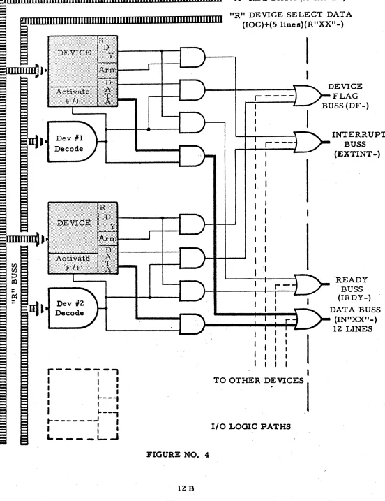
During the execution of any I/O command, the decode OP code (lOP) is routed via a driver inverter to the output connector to form the I/O operation command (IOPB-).
Eijl?(F\~\11¥J
41 61 61
'11
81 91101111
t i t
, :
Operation Code _ 0001The three signals, R4, RS' and R6' representing each bit of the I/O command, are also available on the I/Oconnector andare
pre-sented at the interface as (R04B-), (ROSB-), and (R06B-). These
are decoded by the external device to determine the exact I/O command in order to simplify some interface hardware. The data and status control signals are decoded and presented to the interface as (TTAB-), (TFAB-), (DSTB-), and (SDFB-). All eight of the master CPU timing pulses are supplied to the I/O connector as (RTOB-), (RTlB-), (RT2B-),
(RT3B-)' (RT4B-), (RTSB-), (RT6B-), and (RT7B-). (See Timing
Chart). The complete complement of timing is presented to allow the external device to manipulate data within its controller at any
conven-ient time period with relation to the CPU timing requirement. The
five bits of the device select code are decoded by the external device to determine the device which is to respond to the I/O command. These are presented as buffered data bits from the R Register (R07B-), (R08B-), (R09B-), (RIOB-), and (RllB-).
In order to carry out the SCC "open end" design philosophy, attention should be directed to the high order device commands EXU (100), TMR (101), SEL (110), and IOC (Ill). The EXU (execute com-mand in A) requests the external device to look to the A Register for a command word. Since the CPU generates no function except the I/O op code decode, and requires no signal from the device, all high order commands may be interpreted one of two ways.
These high order commands may be used simply as four indi-vidual one instruction commands to the external device or may, accord-ing to system requirements, direct the device group addressed to look to the accumulator for further, or second order, instructions.
(0607)8
Example of a first order I/O instruction:
Arm interrupt control for card
read-er. This allows the card reader to
interrupt on reading a card segment· and being ready for information
trans-fer. This does not require a
Example of second order I/O instruction:
(0772)8 SEL, Digital Channel Activate digital channel #(4003)8 to
accept next T FA, Digital Channel (0072)8 data, upon accepting that data
hold the value and return to I' stand
by off line" until commanded again. It should be noted that th,is instruc-tion (SEL) normally doe s not look to the A Register for part of its control code, but as in this case, can be di-rected by hardware to do so.
I/O COMMANDS AND TIMING
The symbol "XX" means any or all of specific bits of a register,
i. e., R Register bit 3 would be R03; any bit of the R Register would
be R"XX".
Transmit to A
TimeAnd
Condition Function
T2· lOP Set Device Ready Line (IDRDY)
if ready and gate data to input Bus s UN"XX")
T 4' IDR DY Set internal ready condition DRDY
TS· DRDY Clear Accumulator
T6· DRDY Transfer input to Accumulator
and set Skip F
/F
if device readyT7·
rop
Clear (IDRDY) - Buss clear databuss
Transmit From A
T2· lOP Data available for transfer of
accumulator data to external device. Set (IDRDY) Buss low if device ready
Performed By
External Device
Computer
Computer
Computer
External Device
I/O Commands & Timing
(Transmit From A, continued)
Time And
Condition Function
T4· IDRDY Set internal ready condition (DRDY)
T 5· DRDY Set Skip F /F if device ready
T6· lOP Clear IDRDY - Buss
Input Device Status To A
T2· Gate Status data to Input Lines
(IN''XX")and set lDRDY - Buss low
T4· IDRDY - Set internal ready condition (DRDY)
T5· DRDY
T6· DRDY
T7· lOP
Clear Accumulator
Transfer input lines into Accumulator
lDRDY - Bus s clear
Skip On Devic e Flag
T2· lOP
T5· DF
T7· lOP
Set Device Flag (DF-) low (0 volts),
Set Skip F /F if Device Flag (DF-) is low
Clear Device Flag Bus s (DF -)
Execute Command In A
T2' lOP
T6· lOP
T7
Clear Device Command Register
Transfer Accumulator into Device Command Register
Remove I/O Command
Performed By
Computer
Computer
External Device
External Device
Computer
Computer
Computer
Exte rnal Devic e
External Device
Computer
External Device
External Device
External Device
110 Commands & Timing Time And
Condition Function Performed
By
Terminate
T2· lOP Clear Device Activate F /F External Device
T7 Remove I/O Command Computer
Select
T2· lOP Set Device Activate F /F External Device
T7 Remove I/O Command Computer
I/O Control
T2· lOP Set I/O Control Activate F/F External Device
T7 Remove I/O Command Computer
Two signals are required by the computer from the external device. They are:
1. Device Flag. This signal is tested by the computer
skip-on-device flag command. (SDF or I/O Command 011). Skip (P+2-t ~
if flag (DF-) is +8 V; otherwise (DF-
=
OV) P +1 .... P.2. Device Ready (DRDY-). This signal conditions the com-puter transfer on:
a) Transmit to Accumulator (TT A or
II
0 Command 000)b) Transmit from Accumulator (TFA or I/O Command 001)
c) Input device status to Accumulator (DSTor I/O Com-mand 010).
These transfers are not completed and the skip will occur
un-less device-ready signal is present. That is, DRDY -
=
a v,
P+l, .... P;Both device flag and device ready must be set true at the CPU prior to (RT4B-) and cleared no earlier than (RT6B-). The (RT2B-) and (RT6B-) may be used to synchronize the turning on and off of de-vice flag and dede-vice ready flip-flops.
A signal is provided DEVICE READY F/F BUFFERED (DRDYB-) to notify the external device controller that the Devi{1e Ready Flip-Flop within the computer is set, the CPU will not skip the next instruction and data transfer will occur. The TTA, TFA, SDF, DST instructions are organized so that they will skip the next instruction if the device is NOT ready (skip if not ready). This allows a test for the source of
interrupts by TTA and jump instructions only. An example interrupt
RTOB- RTIB- RT2B- RT3B- RT4B- RT5B- RT6B- RT7B-
R"XX"B-!
;-lrl
I
I-ls---
U
-I
I
onJ
I
I
I
I i
I
I
I-I
I
I
I
i
I
I
~
II
I
-irl
I I, I I
u
I IJ
I
I
IOPB-~
N Instructions
»
(L~Al
I
fI
I
I i I
I I
I
LDA-A Register Out put
A"XX"B-Transfer Input to a ~eg
ternc
Clear A Reg (In 1.1)
- '0
TFAB-
TTAB-Device Ready' IDRDY - (II!put)
DRDYB- (Outpu
or DF-I
t)
I
..zt
ro
(Intel
f -
~
iIf
v .uS€
!
I
I
I
I
I0 [ne;
sJ
gn1
1lI
I
I
na I
I
I
I
I
I
I
I
J
I
I I
i '1
d)
I
II
I
!
I I
II
I! ; i
I
,
I;
I
1-
U--
~
I-
~
!I
!
I
-
U-
I-
~I
I-irl
I,
U
II
J
I
I
J
I
(T
FiAlI
i,
I
I
I
I
I II
I I I II
I I':T~t11
l~tB?
II
I
I I I!
i I ! I ! !
I
I
i
W-
I II-I
W--
Lr
I
-
W-j
-
u:
I
i-Wi
I
I
-
Lr
-
U
I
-
W-
I
I-V
I-
~
I i -,
l.J
1-11
Il.J
I
J
n
!
I
'jI I
I
I
(~O~\
I I
I ,
I (TIT AlI
, II I
I
I
I
~i
I one:
I
I
I
I
I
n
1
I I
I
I
I
I
I
n
II I I
I
II
I
I
II
I
1 I
I
I
I
I
i I!
I 1
I
Il
I
!
I
I
I
I
iI
I I ; i iI
I
\vlll
!fr
ns····
... f::'.::::.'
t
I
~::~ ~~ :~~::~~~~:.I
I; .1
I
!
I
,
I
I I
I
I
I
I I
I
I
I
I
I I t
\
I
I
-"A" REG DATA (A"XX"B-)
"R" DEVICE SELECT DATA (IOC)+(5 lines)(R"XX"-)
I
I
" " " DEVICE
r ---:)
~FLAGI - BUSS (DF-)
:
I
I
~
INTERRUPT• neV#I)
Decode
"""'--_ _ _
- -____ ....
_ , )
-: r---j . /
BUSSI ---- (EXTINT - )
I
~
DevIIZ""\ '
DeCOdeJ
r----,-'
I
II I I
I
~---:
I I I
I
a..--,
t---'
I
I
: .
L _ _ _ _
l...-..I
I
I
I
I
-
I
I
I
,
I
I
I
'I
-
'. r _ - J R E A D Y~~---r-r-r--~~ BUSS
: I : - . (IRDY-)
-FIGURE NO.4
I
I '~ DATA BUSS: I I . - , . / (IN"XX"-)
-,
1._
12 LINESI
TO OTHER D~VIGES
I
[image:21.612.42.594.44.761.2]INTERRUPT
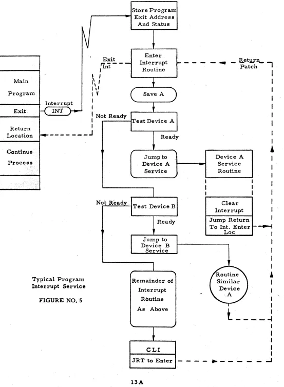
An input is provided (EXTINT-) for interrupt of the machine by the external devices. This input, when taken to 0 volts, will cause an indirect jump and store location to the interrupt trap location and from there to the interrupt service subroutine. This indirect trap allows an interrupt to variable locations during a program. A return to the main program from an interrupt is accomplished by a
subrou-tine return jump JRT to the address located in the interrupt trap
lo-cation. All exits from interrupt routines should be preceeded by a
clear interrupt instruction eLI since the interrupt control will not allow another interrupt of the same level until the current interrupt
is proce s sed. If there is an interrupt awaiting the completion of an
earlier interrupt to be processed, the interrupt control will exit from the current interrupt subroutine, and return to the main program for
one instruction before servicing the waiting interrupt. This feature
allows the main program to proceed at a reduced rate, even if it has continuous interrupts.
If the interrupt input line (EXTINT-) is activated (EXTINT=O Volts) before T2 (RT3B-), the interrupt will be processed at the next T4 pulse (RT4B-) of the next instruction fetch phase if the interrupt subsystem is enabled.
The interrupt subsystem may be disabled or enabled under pro-gram control by SIN (0322)8, set on; and SIF (0222)8, set off. The terrupt control may also be overridden to an "on" condition by the in-terrupt enable button on the console. When the inin-terrupt is enabled by the console, the program may not disable the interrupt subsystem.
Main
Program
Interrupt
Exit.
K
INT)-t--Store Program
1,---...
Exit Address And StatusExit
r:r----,Int~\
I
I \
II ,I
I
~I
I
Enter. Interrupt
Routine
Save A )
I
Not ReadyI ,.---fTest Device A
I
---.
- B.etllIhl\.- .,.Patc
I
I
Return
Location
r.--- ___
.J
ReadyI
Continue
Process
[image:23.612.41.594.25.779.2]Typical Program Interrupt Service
FIGURE NO.5
I.
rJump to Device A
Service
Not Ready, Test Device B
Ready
,
Jump to Device B
Service
Remainder of
Interrupt
Routine
As Above
eLI
JRT to Enter
.
Device A Service Routine
Clear
Interrupt
Jump Return To Int. Enter
Loc
..
-
-Routine
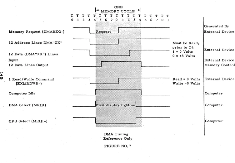
DIRECT MEMORY ACCESS
Direct Memory Access Feature. The direct memory access
feature permits high speed data transfer between memory and external devices. This access channel operates on a "cycle stealing" basis. As. a result, the external device is not required to wait until the present instruction is complete before control of the memory is transferred to . the external device. The DMA does not necessarily defer the program in the CPU if the CPU is not requesting memory for that cycle. If the CPU is executing non - memory instructions (I/O, MICRO OPR, etc.), the CPuwill not idle and wait for DMA release control. Complete isolation between memory banks allows the computer to continue undisturbed if the external device reque sts a memory bank other than the one being used by the processor. The CPU is deferredonly if both it and the DMA require the same memory bank, in which case, the DMA has a priority over the CPU.
Direct Memory Access Transfers. External devices connected to the computer's direct memory access channel have priority over
in-ternal computer operations. Synchronization requires a maximum of
one computer cycle. A direct memory access is initiated by the
ex-ternal device giving a memory request- -setting the memory request
line (DMAREQ-) to 0 Volts--to the computer. Each block or bank of
4,096 words of memory is requested separately through the DMA entry of that memory bank from which the data is to be entered or extracted. The external device must supply to the DMA channel 12 bits of address (DMA"XX"-), 12 bits of data (DMD"XX"-), a read/write line (EXMRDWR-) for +8V,for read, 0 volts for write, and the memory request (DMAREQ-) +8V no request, 0 volts for access request. (See diagram of DMA entry).
All signals into the DMA connector should be settled by T4 of the computer cycle and will always be completely processed at the
first T4 pulse following the DMA request. Data, address, and read /
write signals should remain until the following TO.
Interface Connector
'1EXMRDWR-»
.. (EXMROl-) )
12 Lines
CPU to Memory Data - 12 Lines
CPU to Memo Address
12 Lines
CPU Memory
Enable ....-. .... (SYNCA1)
Inhibit FromDMA
5 (MRQl-)
.. (DMA "XX''-) )
DMA Address
12 Lines
.. (DMD"XX"-) )
DMA Data In
(MRQl-) Inhibit CPU
Memory Request
DMA Has
Memo Control
1 Line (MROIB-)
... (EXD"XX"
-»
12 Lines
(R"XX"-)
(D"XX" -)
(S"XX"-)
est
,...
..
Memory Request (DMAREQ-)
12 Address Lines DMA"XX"
12 Data (DMA"XXtl) Lines
Input
12 Data Lines Output
tJJ - 1 Read/Write Command (EXMRDWR-)
Computer Idle
DMA Select (MRQl)
CPU Select (MRQl-)
T T T T
o
1 2 3ONE
J..-MEMORY CYCLE
~
T T
Z
...
DMA Timing Reference Only
T T
3 4
T T T T T
5 6 7 0 1
Must be Ready prior to T4
1
=
0 Voltso
=
+8 VoltsGenerated By
External Device
External Device
External Device Memory Control
Read
=
8 Volts External DeviceWrite -0 Volts
Computer
Computer
[image:26.792.20.772.54.577.2]LOGIC CIRCUITS
All signals from the computer to be used by external de-vices are isolated from the internal computer logic by the use of driver
inverters. These drivers are included in all 650 - 2 standard logic.
The internal CPU logic voltages are +8 volts DC true and 0 volts DC false for standard NAND gate logic, Signals from -the external device to the computer at the interface are used by the computer as low true logic or "1".= OV, "O"=+8V, The input (Type N) an~ output (Type DI) logic circuits are noted on the interface connector drawings, Figures
15 and 16, Appendix A',
,,---.----..) Output
I
2N36-T'"
1.8K
50 MA
\
a~
\rC.tr.. \
d
12 K
-15V
--6---
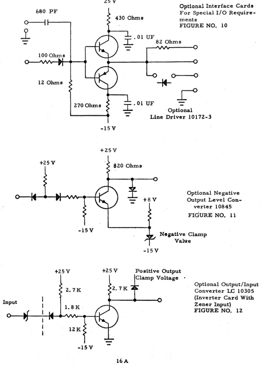
-15 VInputs and outputs from the computer are low true signals. This signal logic was chosen for two reasons:. The input circuits will
lines. The second reason is to allow customers who wish to do the interface logic for their special applications to use descrete or inte-grated circuit logic which has an NPN transistor element on the out-put. By allowing low true, NPN output, logic can, through a saturated transistor, pull down input lines quickly and "sink" the line capacity.
For special applications, the optional line driver 101 72- 3 is available to drive long lines or to match the output circuits to inter-face lines. See Figure 10. Also available for level conversion at the
, interface are the optional negative and positi~e level converter s 10845
Input
680 PF
O~---t __
___
.1
100 Ohms
12 Ohms
25V
430 Ohms
Optional Interface Cards ·For Special I/O
Require-menta
FIGURE NO. 10
.01 UF
I..
82 Ohms0--0--.10
*
270 Ohms
-15V
+2SV
2.7 K
12K
-
. Optional-
Line Driver 10172-3-15V
+25V
820 Ohms
+25V
f8V
Optional N e gati ve Output Level
[image:29.615.59.592.32.776.2]Con-verter l0845
FIGURE NO. 11
Negative Clamp Va lu" e
-15V
Po siti ve Output Clamp Voltage .
Optional Output/Input Converter 1..C 10305 (Inverter Card With Zener Input)
MECHANICAL CHARACTERISTICS
The basic
sec
650 is housed in a standard cabinet with ashadow box trim front and removable sides. The front opening space
is 70 inches of panel space. For dimensions, see Figure 13. Other
special optional configurations available for the
sec
650 are casterbase for mobility, ruggedized slide mount for van applications, and desk configuration where modern formal dress is important. Other special configurations will be considered.
ELECTRICAL CHARACTERISTICS
The SCC 650 requires l15V AC, 60 cycle, ~ AMP,
pri-mary, sing~e phase power. Any additional power required from the
controlled AC power Bus s within the CPU should be added for sy stem requirements.
Internally, the CPU power supply furnishes t25V, tlOV, +8V, and -ISV. The low tlOV is used for lamp and display power and the other supplies are used for the logic cards.
PHYSICAL DIMENSIONS FIGURE NO. 13
28-3/4"
1
- 24"---j
All interface connections to the SCC 650 are made to the rear panel connector plate. This panel is located at the lower rear of
the cabinet. On this panel are located the DMA, I/O, analog, and AC
power connector s as shown below.
The interface connector s for the I/O and DMA are ELCO 56 pin connectors (ELCO #00-8016-056-000-007). The mating connec-tor is ELCO #00-8016-056-000-003. The optional analog connecconnec-tors
m
BNC panel mounts, type UG492 A/U bulkhead adapters and willaccept any BNC cable mate s.
The AC power is brought in through a Hubbell #7327 twist lock male base. The mating connector is a Hubbell #7313 female con-nector with #12 wire for line cord.
There are four parallel I/O connectors with pin configu-ration as shown in Figure 15, Appendix A.
N
=
Input LogicDI
=
Output LogicSIGNAL INOO-INO 1- IN02- IN03- IN04- IN05- IN06- IN07- IN08- IN09- INI0-IN 11- ACOOB- ACOIB- AC02B- AC03B- AC04B- AC05B- AC06B- AC07B- AC08B- AC09B- ACIOB- ACIIB-ZEROB082 ZEROB083
ZERO BOBl
ZERO B081
IN PUT / 0 U T PUT - APPENDIX A
PIN· ASSIGNMENTS
UNIT 650-2
CONN J-I04 TYPE 8016-056 FIGURE NO. 15
LOGIC FUNCTION PIN CODE
Data
Innut A N
"
B N"
C N"
D N,
"
E N"
F N"
H N"
J N"
K N"
L N"
M N"
N N DataOutput P DI
II R DI
"
S DI"
T DI"
U DI"
V DIII W DI
"
X DIIi Y DI
"
Z DI"
a DI"
b DIGND c
-tt d
-"
e"
flost Reg
LOGIC
SIGNAL FUNCTION PIN CODE
~nst .Keg
RO"6B- Output k DI
R07B-
"
1 DIR08B-
"
rn DIR09B-
"
n DIRIOB-
"
p DI_~IIB-
"
r DI I/OIOE- Error s N
I
t
RTIB- Timin~ u DI
RT3B-
"
v DIRT4B-
"
w DIRT5B-
"
x DIRT7B-
"
y DISTCLEAR- Start z DI
EXTINT- Interrupt AA N
SDFB- I/O OPS BB DI
DSTB-
"
CC DITFAB-
"
DD DITTAB-
"
EE DI
-DRDYB- . Device
JOutput) Rp~("hT FF DI
RTOB- Timing
HH
DIRT2B-
"
JJ DI.
RT6B-
"
KK
DII/O
IOPB- lnst. LL DI
Device
DF- Flag MM N
ID&DY ... DevIce
[image:33.621.52.592.36.767.2]N
=
Input LogicDI
=
Output LogicSIGNAL DMDOO- DMDOl- DMD02- DMD03- DMD04- DMD05- DMD06- DMD07- DMD08- DMD09- DMDIO- DMDll- DMAOO- DMAOl- DMA02- DMA03- DMA04- DMA05- DMA06- DMA07- DMA08- DMA09- DMAIO- DMA11-STCLEAR
ZERO C28
ZERO C28
ZERO C28
ZERO C28
DIRECT MEMOR Y ACCESS - APPENDIX A
PIN ASSIGNMENTS
UNIT 650-2
CONN J-I05 TYPE 8016-056 FIGURE NO. 16
LOGIC LOGIC
FUNCTION PIN CODE SIGNAL FUNCTION PIN CODE
Data
Input A N
Data
EXDOO- Output k DI
"
B N EXDOl-"
1 DI"
C N EXD02- II m DI"
D N EXD03-"
n DI"
E N EXD04-"
p DI"
F N EXD05-"
r DI"
H
N EXD06-"
s DI"
J N EXD07-"
t DI"
K
N EXD08-"
u DI"
L N EXD09-"
v DI"
M N EXD10-"
w DI"
N N E XD11-"
x DIAddress
Input P N RTIB- Timing y DI
Ii R N RT3B~ Ii z DI
"
S N RT4B-"
AA Dr"
T N RT5B-"
BB DII'
U N RT7B-"
CC Dr"
V N EXTINT- Interrupt· DD N Read/Write"
W N EXMRDWR- Control EE N"
X N FF"
y NHH
11 Z N
JJ
"
a N EXMRQl- .DMA RequestKK
N"
b N RTOB- Timing LL DIStart c DI RT2B-
"
MM
DIGND d
-
RT6B-"
NN DI"
e-"
f [image:34.613.50.577.48.775.2]APPENDIX A
INTERFACE SIGNATURE DEFINITIONS
L ACOOB through ACIIB
2. DF
3. DMAOO through DMAII
4. DMDOO through DMDll
5. DRDYB
This signature is the I/O accumulator outputs. They are the buffered
accum-ulato r output data Bu s s line sand
appear at the connector as low True Signals. The se data buffer s pre sent the contents of the accumulator to the I/O connector at all times.
This is the I/O interface input to the
CPU for the device flag Buss. For
the I/O instruction, II skip no device
flag" (SDF), this signature must be taken to 0 volts for the central pro-cessor to execute the next instruction. Otherwise, the central processor will skip the next instruction on an SDF instruction.
The se are the external DMA addre s s input lines provided by the external interface to provide the DMA control unit with addressing for the memory
unit. These lines must be present
during either DMA read or DMA write (Input).
The se are the signature s provided by the external DMA to provide the DMA input control with data to be input into the memory (Input).
This signature is a buffered internal' device ready signal from the central
processor to the I/O interface. It
6. DSTB
7. EXDOO through EXDll
8. EXMRDWR
9.
EXMRQI10. EXTINT
11. IDRD'X'
This is the decode of 11 input device
status" (DST) I/O operation code. To completely provide the I/O DST, it is
conditioned with
rop.
The se are the line s provided by the DMA control for the external DMA interface to receive the data from the memory during a read cycle (Output).
This signature is "external memory read/write ff and is the single line
in-put provided by the DMA for the direct memory access read / write control line. When this signature is taken to
o
volts by the external connector, thememory will be in a write condition
(Input).
This is the signature provided by the external DMA interface to the DMA control to initiate a DMA cycle. If the external connector takes this sig-nature to 0 volts, it will initiate a di-rect memory access cycle at the next T 4 time interval.
This is the external interrupt signal
line. If the external interface takes
this signature to
a
volts, it williniti-ate an interrupt cycle at the end of the current instruction.
This is the device ready Bus s. It is for the I / 0 interface to input to the central processor that 'the device is
ready. If the interface takes this
signature to 0 volts, it will notify the
central proce s sor during the 110 skip
12. INOO through INII
13. IOE
14. IOPB
15. MRQlB
16. RTOB through RT7B
17. R04B through RilB
This signature is the input data to the CPU and is provided for the external I/O interface to input data to the AC Register. This is a data Bus s for pro-gram data transfer s and the data will be input to the AC under central pro _. ce s sor control.
This signature is for I/O error, and is used by the I/O interface to notify the central processor that there has been an I/O error (parity, fetch,
over-run, etc,). If this signature is taken
to
a
volts by the external connector,the I/O error flip-flop within the status
regist~r will be set and the CPU
noti-fied of the I/O error.
This is the buffered decoded I/O in-struction code. It is decoded from RO through R 3 and is pre sent only when the I/O instruction code (OOO l) 2 is present.
This is the buffered signal notifying the external DMA interface that the central control unit acknowledge s the DMA request and is executing a direct memory access cycle.
The signature s are provided to the in-terface by the CPU timing control unit
and a~e the master control timing for
the central processing unit. These
are available to direct memory access andI/Ofor external synchronous tim-ing and control use (Output).
The se signals are the buffered instruc ...
tion register outputs to the
I/o
18. SDFB
19. TFAB
20. TTAB
. 21. ZERO
This is the buffered decode of skip no device flag and is a decode of R4 thru
R
6
of the instruction register.. Forthe interface to completely provide the skip on device flag OP code, this sig-nal is conditioned with lOP.
This is the buffered decode of the TF A
instruction. It is decoded from R4
through R 6 and to completely provide
the I
I
OTFA, it is conditioned withlOP in the CPU.
This is the buffered decode of the "Transmit to A" (TFA)
II
0 instructionOP code. It is decoded from R4 thru
R 6 and to be completely conditioned,
it is gated with
rop
in the centralpro-cessor .
This is a ground return or ground wire from the central processor power con ..
trol unit. It is 0 volts and may be used
for grounding external devices, 0 r
APPENDIX B
ASCII CODES AS THEY' APPEAR IN "A" REGISTER
LOWER "A" LOWER "A" LOWER "A"
CASE REGISTER CASE REGISTER CASE REGISTER
A 0101 W 0327 ( 0333
B 0102 X 0330
"
0134C 0303 Y 0131
]
0335D 0104 Z 0132
,
0336E 0305 LF 0012
...
0137F 0306 CR 0215 @ 0300
G 0107
SF
0240 0041H 0110 0254
"
0042I 0311 0055
#
0243J 0312 0056 $ 0044
K 0113
/
02570/0
0245L 0314 0 0060 & 0246
M 0115 1 0261 0047
N 0016 ' 2 0262' 0050
0 0317 3 0063 ) 0251
P 0120 4 0264
+
0053Q, 0321 5 0065
<
0074R 0322 6 0066
=
0275S 0123 7 0267
>
0276T 0324 8 0270 ? 0077
U 0125
9
0071 BELL 0207I
I
SPROCKET_l
..
5 6 7PAJUTY j
2 SPROCKET_ 3
..
S 6 1 PAlUTY 8
.. .
.
IMPULSE POSITION
NULL 80M EOA EOM !:OT WRU RU BELL FEo HT SK LF VTAB FF CR SO SI DCo
t~TORM .... TtOS
SEPARATORS
l~ll+I+I·I'I'I+I·1
-I
11'1'1'1+1+1'1'
1-1·1
H
+1'1
....
.
.
/
UNASSIGNED\
....
AScn 8-LEVEL PAPER TAPE FORMAT
L!:GEND
Null/Idle OCI-De Z Device Control Start of Message OCI (Stop) Device Control (Stop) End of Address ERR Error
End of Message SYNC Synchronous Idle !:nd of Transmission . LEM Logical End of Media "Who 3.re you?" So-St Separator (Information) "Are you •.. ?" b Word Separator (space. Audible Signal normally non-printing) Format Effector Less Than
Horizontal Tabulation Greater Than
Skip (punched card) Up Arrow (Exponentiation) Line Feed Left Arrow (Implies/Re-Vertical Tabulation
\ placed By)
Form Feed Reverse Slant Carriage Return
(fr
Acknowledge Shift Out Unassigned Control Shlft In ESC EscapeAPPENDIX
C
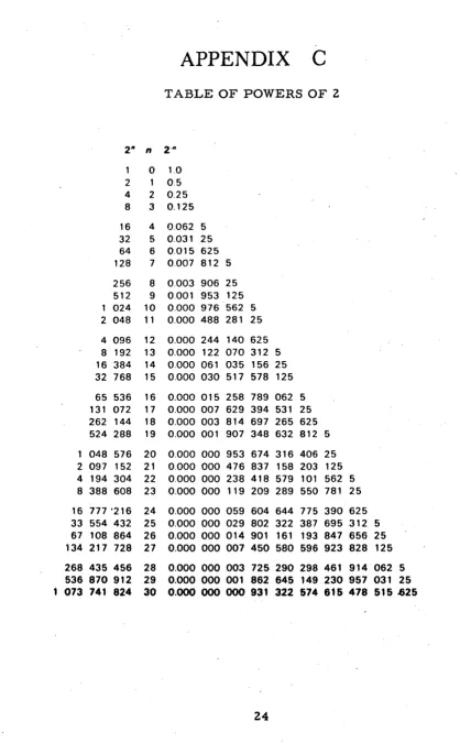
TABLE OF POWERS OF 2
2" n 2'"
1 0 1.0 2 1 0.5 4 2 0.25 8 3 0.125
16 4 0.062 5 32 5 0.031 25 64 6 0.015 625 128 7 0.007 812 5
256 8 0.003 906 25 512 9 0.001 953 125 1 024 10 0.000 976 562 5 2 048 11 0.000 488 281 25
4 096 12 0.000 244 140 625 8 192 13 0.000 122 070 312 5 16 384 14 0.000 061 035 156 25 32 768 15 0.000 030 517 578 125
65 536 16 0.000 015 258 789 062 5 131 072 17 0.000 007 629 394 531 25 262 144 18 0.000 003 814 697 265 625 524 288 19 0.000 001 907 348 632 812 5
048 576 20 0.000 000 953 674 316 406 25 2 097 152 21 0.000 000 476 837 158 203 125 4 194 304 22 0.000 000 238 418 579 101 562 5 8 388 608 23 0.000 000 119 209 289 550 781 25
16 777 '216 24 0.000 000 059 604 644 775 390 625 33 554 432 25 0.000 000 029 802 322 387 695 312 5
67 108 864 26 0.000 000 014 901 161 193 847 656 25 134 217 728 27 0.000 000 007 450 580 596 923 828 125
268 435 456 28 0.000 000 003 725 290 298 461 914 062 5 536 870 912 29 0.000 000 001 862 645 149 230 957 031 25
[image:41.613.71.489.57.732.2]AREAS OF APPLICATION
I. Business and Manufacturing in General
1. Offite Cost analysis Forecasting Inventory control Mailing list operations
Management strategy anal, •• Performance evaluation Price analysis
Purchase order writing Sales forecasting
Wage and salary analysi. Work-in-process records
2. Plant and Production Assembly line balancing
Lathe operations: automatic control Procurement
Production scheduling Quality control records
Route accounting (bakeries, bottling plants, dairies, etc.
3. Libraries
Information retrieval Records and control
4. Magazine Publishing
Classi fied advertisement preparation Mailing list maintenance
Subscription fulfillment
5. Oil Industry
Depletion accounting Map construction Oil purchase accounting Operating records: logging Remote control of oil produetion Seismic data reduction
Well logs: corrections
6. Textile Industry l"abric quality control
Material availability evaluation Production planning
Sales analysis Style reporting
7. Transportation
APPENDIX.-£.
Collision warning systems Navigating systems
Preventive maintenance scheduling Travel reserVations
II. Science and Engineering
1. Aeronautics and Space Engineering Curve fitting
Flight control for missiles and space vehicles Flight simulation
Flight test data reduction Heat transfer analysis Vibration analysis
Wind tunnel data reduction
2. Chemical Engineering and Cheaa'.tr1
Gas line. calculation Process control Spectrum analysis
3. Civil Engineering Abutment design Beam design
Cut and fill calculations Earthwork computations Freeway assignment Highway profiles
Monthly equipment summary Stress analysis
Triangulation
4. Electrical Engineering Component design
Computer logic circuits; design by numerical control
Feedback system, single loop, finding the root locus
6. Mechanical Engineering Air conditioning calculations Heat flow
Machine vibration analysis
6. Medicine and Physiology Telemetering and analysis
of Medical data
Probability in medical diagnosis
SCC maintains complete support activities for its users. Installation and maintenance services are available through SCC offices strategically located throughout the United States. For pre-procure-ment demonstration of hardware and programs in Dallas, contact local sales office or the Marketing Department in Dallas.
Arlington, Massachusetts
30 Park Avenue
617 - 648-2922
(Boston)
Skokie, Illinois
125 Old Orchard Arcade
312 - 675-6700
(Chicago)
Houston, Texas
7800 Westglen Drive
713 - 782-9851
Seattle, Washington
1806 South Bush Place
206 - 324,7911
Midland Park, New Jersey
36 Central Avenue
201 - 652-6750
(New York)
Crofton, Maryland Village Green
301 - 647-6431
(Baltimore)
Orlando, Florida
2319 E. South Street
305 - 841-3556
Pasadena, California
180 East California Blvd.
213 - 681-2651
(Los Angeles)
Other SCC products include: telemetry systems and airborne signal conditioning equipment such as amplifiers, demodulators and converters.