VMIVME-4911
Quad Channel
Synchro/Resolver-to-Digital Input Board with Built-in-Test
© Copyright 2002. The information in this document has been carefully checked and is believed to be entirely reliable. While all reasonable efforts to ensure accuracy have been taken in the preparation of this manual, VMIC assumes no responsibility resulting from omissions or errors in this manual, or from the use of information contained herein.
VMIC reserves the right to make any changes, without notice, to this or any of VMIC’s products to improve reliability, performance, function, or design.
VMIC does not assume any liability arising out of the application or use of any product or circuit described herein; nor does VMIC convey any license under its patent rights or the rights of others.
For warranty and repair policies, refer to VMIC’s Standard Conditions of Sale.
AMXbus, BITMODULE, COSMODULE, DMAbus, IOMax
,
IOWorks Foundation, IOWorks Manager, IOWorks Server, MAGICWARE, MEGAMODULE, PLC ACCELERATOR (ACCELERATION), Quick Link, RTnet, Soft Logic Link, SRTbus, TESTCAL, “The Next Generation PLC”, The PLC Connection, TURBOMODULE, UCLIO, UIOD, UPLC, Visual Soft Logic Control(ler), VMEaccess, VMEbus Access, VMEmanager, VMEmonitor, VMEnet, VMEnet II, and VMEprobe are trademarks and The I/O Experts, The I/O Systems Experts, The Soft Logic Experts, and The Total Solutions Provider are service marks of VMIC.COPYRIGHT AND TRADEMARKS
The I/O man figure, IOWorks, IOWorks man figure, UIOC, Visual IOWorks and the VMIC logo are registered trademarks of VMIC.
ActiveX, Microsoft, Microsoft Access, MS-DOS, Visual Basic, Visual C++, Win32, Windows, Windows NT, and XENIX are registered trademarks of Microsoft Corporation.
MMX is trademarked, Celeron, Intel and Pentium are registered trademarks of Intel Corporation. PICMG and CompactPCI are registered trademarks of PCI Industrial Computer Manufacturers’ Group. Other registered trademarks are the property of their respective owners.
Table of Contents
List of Figures . . . 7
List of Tables . . . 9
Overview . . . 11
Functional Description . . . 12
Reference Material List. . . 14
Safety Summary . . . 15
Ground the System . . . 15
Do Not Operate in an Explosive Atmosphere . . . 15
Keep Away from Live Circuits . . . 15
Do Not Service or Adjust Alone . . . 15
Do Not Substitute Parts or Modify System. . . 15
Dangerous Procedure Warnings . . . 15
Safety Symbols Used in This Manual . . . 16
Chapter 1 - Theory of Operation . . . 17
VMEbus Compatibility Logic . . . 18
Data Transceivers . . . 19
Device Addressing . . . 20
Data Input . . . 21
Synchro/Resolver Board. . . 23
Built-In-Test (BIT) . . . 25
Address Modifiers . . . 31
Jumper Installation . . . 31
Address Selection Switches . . . 31
Example 1: . . . 33
Connectors . . . 34
User Input Cables . . . 34
Front Panel Input Connector P3 . . . 34
VMEbus P2 Connector Pin Assignments . . . 34
Reference Input. . . 34
Chapter 3 - Programming . . . .41
Control and Status Register (CSR) . . . 43
Maintenance . . . 45
Maintenance . . . 45
List of Figures
Figure 1 VMIVME-4911 Functional Block Diagram ... 13
Figure 1-1 VMEbus Compatibility Logic ... 18
Figure 1-2 Address Compare Subsystem Detailed Block Diagram ... 20
Figure 1-3 Simplified Data Input Block Diagram ... 22
Figure 1-4 VMIVME-4911 Synchro/Resolver-to-Digital Converter Modules ... 24
Figure 1-5 Typical Subsystem Configuration for Testing VMIC’s VMIVME-4900 and 4905 Synchro/Resolver Output Boards ... 25
Figure 1-6 VMIVME-4911 Power Subsystem Block Diagram ... 26
Figure 2-1 Location of Jumpers and Switches ... 32
Figure 2-2 Address Select Switches ... 33
Figure 2-3 Typical Input Configuration ... 35
Figure 2-4 P2 Connector - Pin Layout ... 39
List of Tables
Table 1-1 Data Input Word: Bit Weight. . . 21
Table 2-1 Jumper Configuration. . . 36
Table 2-2 Jumper Configuration Continued. . . 37
Table 2-3 P3 Connector Pin Assignments . . . 38
Table 2-4 P2 Connector Pin Assignments . . . 40
Table 3-1 CSR Format. . . 43
Overview
Contents
Functional Description . . . 12
Reference Material List . . . 14
Safety Summary . . . 15
Safety Symbols Used in This Manual . . . 16
Introduction
The VMIVME-4911 is a VMEbus compatible quad channel synchro/resolver-to-digital converter input board which utilizes one synchro/resolver-to-digital module and a quad multiplexer to convert synchro/resolver data to a 14-bit digital word. Features of the VMIVME-4911 Synchro/Resolver-to-Digital Board include the following:
• Synchro or resolver inputs • 14-bit accuracy
• Jumper programmed input selection receives synchro/resolver inputs from the field connector or from the Synchro/Resolver Test Bus Backplane (SRTbus™) for channel zero.
• 26 Vrms or 115 Vrms reference excitation level (option dependent).
• Jumper selection of ±15 VDC power and reference voltage input from test backplane or I/O field connector.
• Supports Built-in-Test on digital-to-synchro/resolver modules with channel zero jumper option.
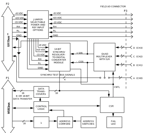
Functional Description
This paragraph describes the functional operation of the VMIVME-4911
Synchro/Resolver-to-Digital Input Board. The synchro/resolver-to-digital converter board consists of VMEbus compatibility logic, a synchro/resolver converter, a quad multiplexer, power input jumper selection, and jumper input selection to support Built-in-Test capabilities, as shown in Figure 1.1-1. The VMEbus compatibility logic contains address selection logic and data transfer logic providing for 8- or 16-bit data transfers. Jumper selection logic provides an option for channel 0 synchro/resolver signals to be sourced from the P3 I/O connector or from the P2 connector via the Synchro/Resolver Test Bus Backplane (SRTbus™). In addition, the ±15 VDC power supply can be jumpered to select P3 I/O connector input or the SRTbus™ input. The synchro/resolver-to-digital input board converts the input of the user's synchro or resolver to a digital format. The board accepts synchro or resolver inputs of 11.8 volts rms line-to-line, 90 volts rms line-to-line, or resolver inputs of 26 volts rms line-to-line. Each of the three variations of the board are available with 14-bit resolution. The user options are given in document number 800-004911-000.
Overview
Figure 1 VMIVME-4911 Functional Block Diagram
P2 +5 VDC +15 VDC -15 VDC RH RL GND JUMPER SELECTABLE POWER AND REF INPUT OPTIONS +5 VDC +15 VDC -15 VDC RH RL GND
FIELD I/O CONNECTOR
P3 SYNCHRO/ RESOLVER- TO-DIGITAL CONVERTER MODULE +5 VDC +15 VDC -15 VDC RH RL GND CSR DATA TRANS- CEIVERS 16
8- OR 16-BIT DATA TRANSFER 16 16 CONTROL LOGIC ADDRESS COMPARE ADDRESS SWITCHES SYNCHRO TEST BUS SIGNALS
Reference Material List
For a detailed description of the VMEbus, refer to The VMEbus Specification and Handbook available from:
VMEbus International Trade Association (VITA) 7825 Gelding Dr. Suite No. 104
Scottsdale, AZ 85620-3415 (602) 951-8866
Fax: (602) 951-0720 e-mail: [email protected] Internet: www.vita.com
Physical Description and Specifications, refer to Product Specification, 800-004911-000 available from:
VMIC
12090 South Memorial Pkwy. Huntsville, AL 35803-3308, USA (256) 880-0444
(800) 322-3616 FAX: (256) 882-0859 www.vmic.com
The following Application and Configuration Guides are available from VMIC to assist the user in the selection, specification, and implementation of systems based on VMIC’s products.
Title Document No.
Digital Input Board Application Guide 825-000000-000
Change-of-State Application Guide 825-000000-002
Digital I/O (with Built-in-Test) Product Line Description 825-000000-003
Synchro/Resolver (Built-in-Test) Subsystem Configuration Guide
825-000000-004
Analog I/O Products (with Built-in-Test) Configuration Guide 825-000000-005
Overview
Safety Summary
The following general safety precautions must be observed during all phases of the operation, service, and repair of this product. Failure to comply with these
precautions or with specific warnings elsewhere in this manual violates safety standards of design, manufacture, and intended use of this product.
VMIC assumes no liability for the customer’s failure to comply with these requirements.
Ground the System
To minimize shock hazard, the chassis and system cabinet must be connected to an electrical ground. A three-conductor AC power cable should be used. The power cable must either be plugged into an approved three-contact electrical outlet or used with a three-contact to two-contact adapter with the grounding wire (green) firmly connected to an electrical ground (safety ground) at the power outlet.
Do Not Operate in an Explosive Atmosphere
Do not operate the system in the presence of flammable gases or fumes. Operation of any electrical system in such an environment constitutes a definite safety hazard.
Keep Away from Live Circuits
Operating personnel must not remove product covers. Component replacement and internal adjustments must be made by qualified maintenance personnel. Do not replace components with power cable connected. Under certain conditions,
dangerous voltages may exist even with the power cable removed. To avoid injuries, always disconnect power and discharge circuits before touching them.
Do Not Service or Adjust Alone
Do not attempt internal service or adjustment unless another person, capable of rendering first aid and resuscitation, is present.
Do Not Substitute Parts or Modify System
Because of the danger of introducing additional hazards, do not install substitute parts or perform any unauthorized modification to the product. Return the product to VMIC for service and repair to ensure that safety features are maintained.
Dangerous Procedure Warnings
Safety Symbols Used in This Manual
STOP:
This
symbol informs the operator the that a practice or procedure should not be performed.Actions could result in injury or death to personnel, or could result in damage to or destruction of part or all of the system.WARNING: This sign denotes a hazard. It calls attention to a procedure, a practice, a condition, which, if not correctly performed or adhered to, could result in injury or death to personnel.
CAUTION: This sign denotes a hazard. It calls attention to an operating procedure, a practice, or a condition, which, if not correctly performed or adhered to, could result in damage to or destruction of part or all of the system.
CHAPTER
Theory of Operation
Contents
VMEbus Compatibility Logic . . . 18
Data Transceivers . . . 19
Device Addressing . . . 20
Data Input . . . 21
Synchro/Resolver Board . . . 23
Built-In-Test (BIT) . . . 25
Reference Input . . . . 27
Introduction
The VMIVME-4911 quad channel board utilizes a multiplexed S/D or R/D converter that can be used when multiple synchro or resolver inputs are sampled for digital computation or display. Multiplexing is found in data logging systems, process monitors, ordnance aiming controls, navigation systems, numerical control, and range instrumentation. The synchro and resolver inputs often represent variables which are analyzed by a computer for monitoring or control.
VMEbus Compatibility Logic
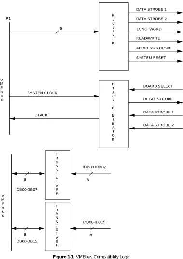
Typical VMEbus drivers, receivers and control logic are shown in Figure 1-1 below.
R E C E I V E R
DATA STROBE 1
DATA STROBE 2
LONG WORD READ/WRITE ADDRESS STROBE SYSTEM RESET BOARD SELECT DELAY STROBE
DATA STROBE 1
[image:18.612.99.478.148.682.2]Data Transceivers
1
Data Transceivers
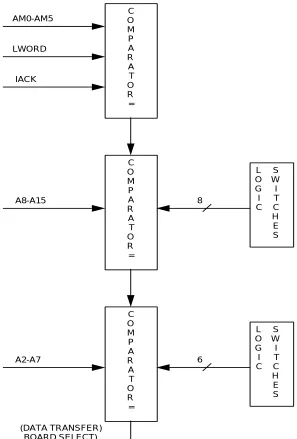
Device Addressing
The VMIVME-4911 is designed to support data transfers in supervisory and/or non-privileged short I/O memory space. The board is factory configured via a
programmed PAL to respond to either of two address modifier codes: Short Supervisory ($2D) and Short Non-Privileged access ($29).
[image:20.612.140.437.230.669.2]Data Input
1
Data Input
A data input operation is initiated when a CPU executes an instruction that sends the VMIVME-4911 board an address that selects the board. During the instruction execution, VMEbus control signals cause the board to place a data input word on the VMEbus backplane data lines to be read by the CPU.
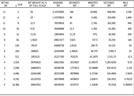
Data input words are digital representations of the corresponding user input signal. User input signal changes will result in continuous variations of the input data which represents the user’s synchro/resolver shaft position. The input data word is a bit pattern that represents the position of the user’s transducer shaft. The associated weighting of each bit is listed in Table 1-1 below.
A simplified functional block diagram of the data input logic is shown in Figure 1-3 on page 22. A data buffer isolates the synchro/resolver data lines from the
[image:21.612.95.554.332.663.2]bidirectional internal data bus (DBXX) which is also used to load data in the control register. The outputs of the control register provide the control for the synchro/ resolver module and the front panel Fail LED.
Table 1-1 Data Input Word: Bit Weight
2
BIT WEIGHT AS % OF FULL SCALE
VMIVME-4911 Quad Channe l Sy nc hro /Res olv e r-t o-Di gi tal Input B o ard w ith BIT F igur e 1-3 Sim p lifie d Da ta In pu t Blo c k Dia g ram TRANSCEIVERS DATA BUFFER CONVERTER MODULE GDSIL GDSOL READ CSRL
D00-D15 DB00-15 DB00-13
[image:22.612.75.707.112.482.2]Synchro/Resolver Board
1
Synchro/Resolver Board
Each multiplexed system, as shown in Figure 1-4 on page 24, consists of one converter module and one or more signal input modules. The block diagram shows one input module connected to one converter module. The input module contains four signal input channels A, B, C, D and one reference input channel.
Each synchro or resolver is connected to a separate input channel, and the reference to the reference channel. The input circuit is either a resolver isolation transformer or a Scott-T transformer.
If several synchro or resolvers share a reference, they will also share a reference input channel. The purpose of the reference input channel is to produce the sample time pulse ST. Each ST pulse causes the dual sample/holds to which it is connected to sample the synchro or resolver input in that channel.
The sample enable, SE, inhibits the sample time generator. If the SE is at logic "one", the sample time generator automatically produces an ST pulse near each positive peak of the reference waveform. The synchro and resolver inputs connected to each reference are therefore sampled simultaneously once during each cycle, unless an SE pulse is applied TheST pulse is inhibited only if the SE is at logic "zero" at the moment the ST is initiated; once the ST begins, a subsequent SE drop to logic "zero" will not affect the ST pulse completion.
The outputs from each signal sample/hold circuit are nominally +4.1 sin Ø sin wt and -4.1 cos Ø sin wt. These signals are sampled by the dual sample/hold at a time close to the positive peaks of the reference waveform. The dual sample/hold outputs are nominally +4.1 sin Ø and -4.1 cos Ø. These outputs are MUXED together to the central converter input. The MUX select lines MA, MB, determine which of these outputs will be processed. The MUX shorting switches are operated automatically by the converter busy pulse to discharge the central converter MUXED input lines between conversions.
The SIN/COS (S/C) select was designed for situations in which the output from a signal module is processed not by a converter module, but by some other means such as a computer. By operating the S/C control, the sin Ø and cos Ø information can be MUXED into one output line.
VMIVME-4911 Quad Channe l Sy nc hro /Res olv e r-t o-Di gi tal Input B o ard w ith BIT Figure 1-4 VM IVME-491 1 Syn c h ro/R e s o lv e r-to-D igit a l C o nv erte r Mo INPUT A SYNCHRO OR RESOLVER SAMPLE TIME STA MA MUX SELECT INPUT D SYNCHRO OR RESOLVER SAMPLE TIME STD MD MUX SELECT A D INPUT CIRCUIT DUAL SAMPLE AND HOLD +S -C +S -C MUX INPUT CIRCUIT DUAL SAMPLE AND HOLD +S -C +S -C MUX +SIN Ø -COS Ø "0" "1" SIN/COS SELECT S/C REF INPUT RH
RL TRANSFORMER ISOLATION
-85˚ PHASE SHIFT RH RL ZERO CROSSING PRECISION CONTROL TRANSFORMER CONTAINS FOUR SIGNAL CHANNELS (A, B, C, D)
AND ONE REFERENCE CHANNEL
+SIN Ø
-COS Ø MUX SHORTING
SWITCHES SIN (Ø-ß)
14-BIT SUCCESSIVE APPROXIMATION REGISTER
(CONTAINS ANGLE Ø)
[image:24.612.82.715.71.497.2]Built-In-Test (BIT)
1
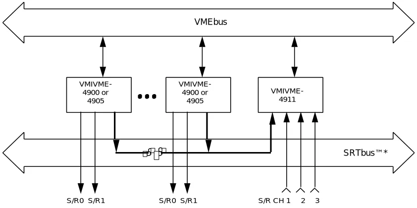
Built-In-Test (BIT)
The VMIVME-4911 is designed such that Channel A may be jumpered to the P2 backplane such that the board can be loop-tested via VMIC's SRTbus™ and Digital-to-Synchro Converter Boards, as shown in Figure 1-5 below. This concept provides the user with the capability to design systems with off-line and on-line fault detection and isolation. The reader should refer to VMIC's Synchro/Resolver Subsystem
Configuration Guide (Document No. 825-000000-004) for a thorough explanation of synchro/resolver Built-in-Test concepts.
[image:25.612.113.534.344.554.2]The synchro/resolver input jumper option seen in Figure 1-6 on page 26 implements the two modes of operation for Channel A. With synchro/resolver input connected to the P3 I/O connector, the VMIVME-4911 lends itself to receive synchro/resolver inputs from the front panel of the board via a 25-pin AMP connector, No. 206584-1. The user can also elect to receive Channel A synchro/resolver inputs from the VMIC synchro/resolver backplane via the P2 connector. This configuration lends itself for use with a Digital-to-Synchro/Resolver Converter Board, such as the VMIVME-4900, for test purposes or the user could supply field inputs directly to the P2 connector instead of using the P3 I/O connector (refer to Figure 1-5 below).
Figure 1-5 Typical Subsystem Configuration for Testing VMIC’s VMIVME-4900 and 4905 Synchro/Resolver Output Boards
VMEbus
VMIVME- 4900 or
4905
VMIVME- 4900 or
4905
VMIVME- 4911
SRTbus™*
S/R0 S/R1 S/R0 S/R1 S/R CH 1 2 3
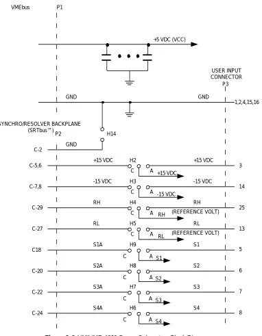
P1 VMEbus GND GND USER INPUT CONNECTOR P2 GND C-2 +15 VDC -15 VDC H2 C A C A C A C A +15 VDC +15 VDC -15 VDC -15 VDC RH RH RH (REFERENCE VOLT) RL H3 H4 H5 H9 H8 H7 H6 RL RL S1A S2A S3A S4A S1 S1 S2 S3 S4 C A C A C A C A S2 S3 S4 C-5,6 C-7,8 C-29 C-27 C18 C-20 C-22 C-24 3 14 25 13 (REFERENCE VOLT) 1,2,4,15,16 +5 VDC (VCC)
[image:26.612.102.484.96.587.2]Reference Input
1
Reference Input
CHAPTER
Configuration and Installation
Contents
Unpacking Procedures . . . 30 Physical Installation . . . 31 Connectors . . . 34
Unpacking Procedures
CAUTION: Some of the components assembled on VMIC’s products may be sensitive to electrostatic discharge and damage may occur on boards that are subjected to a high-energy electrostatic field. When the board is placed on a bench for configuring, etc., it is suggested that conductive material should be inserted under the board to provide a conductive shunt. Unused boards should be stored in the same protective boxes in which they were shipped.
Physical Installation
2
Physical Installation
CAUTION: Do not install or remove the board while power is applied.
De-energize the equipment and insert the board into an appropriate slot of the chassis, while ensuring that the card is properly aligned and oriented in the supporting card guides. Slide the card smoothly forward against the mating connector until firmly seated.
WARNING: Application of reverse polarity to any one of the three power supply inputs will cause catastrophic failure.
Jumper and Switch Locations
Refer to Figure 2-1 on page 32 for the locations of the jumper and switches described in this section.
Address Modifiers
The board is factory configured via a programmed PAL to respond to either of two address modifier codes: Short supervisory ($2D) and short non-privileged access ($29), or both, depending upon the option chosen.
Jumper Installation
Jumpers are provided to connect ± 15 V, RH, RL, and input channels from the front panel (P3) or the P2 connector (Jumpers H2 to H9). Jumpers are also provided for Multiplexer expansion cards (Jumpers H10 to H13 and H1). See Table 2-1 on page 36 for Jumper Configuration.
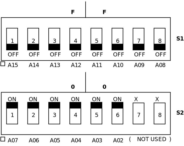
Address Selection Switches
The VMIVME-4911 uses four bytes of the VMEbus, short I/O address space. The upper 14 bits of the short address are Dual-in-Line Package (DIP) switch selectable. The addressing DIP switch and its use in the addressing scheme are shown in Figure 2-2 on page 33
X- Immaterial Switch Position OFF = 1
P1
P2 P3
32 1 1
13
32
1
S2
S1 H1
H9
H8
H7
H6
H5
H4
H3
H2
H11
[image:32.612.91.495.102.607.2]Physical Installation
2
Figure 2-2 Address Select Switches
Example 1:
For the VMIVME-4911 to respond to an address base of FF0016 , the S1 and S2 switches would be set as shown in Figure 2-2 above.
OFF OFF OFF OFF OFF OFF OFF OFF
A15 A14 A13 A12 A11 A10 A09 A08
F F
S1
ON
A07 A06 A05 A04 A03 A02
0 0
S2
ON ON ON ON ON X X
( NOT USED )
1 2 3 4 5 6 7 8
Connectors
The VMIVME-4911 provides a choice of two sources of inputs on channel A,
selectable by jumpers H6, H7, H8, and H9. One input selection uses the P2 connector and operates through the VMIC Synchro/Resolver Backplane. The other source uses the P3 front panel connector (AMP No. 206584-1). A compatible type D cable
connector and strain relief kit is the AMP No. 747322-2. The reader should refer to Figure 2-3 on page 35, Table 2-1 and Table 2-2 on page 37 for signal input selection.
User Input Cables
VMIC recommends the use of shielded, insulated cable, triple-twisted (12 turns per foot) to avoid error inducing conditions at the data and reference inputs.
Front Panel Input Connector P3
The reader should refer to Table 2-3 on page 38 for pin assignments for the front panel user inputs.
VMEbus P2 Connector Pin Assignments
Connector P2, the VMEbus backplane connector may be used for power input, reference input and signal inputs. Connector P2 pin layout is shown in Figure 2-4 on page 39. P2 connector pin assignments are shown in Table 2-4 on page 40.
Reference Input
Connectors
2
S1 A S2 A S3 A S4 A S1 A S2 A S3 A S4 AUSER INPUT CONN P3
SRTbus ™ BACKPLANE P2
INPUT MULTIPLEXER MODULE
ST STA STB STC STD
SAMPLE PULSE L
SEL CH A L SEL CH B L SEL CH C L SEL CH D L EN SAMPLING H MA MB MC MD SE S1 A S2 A S3 A S4 A S1 B S2 B S3 B S4 B S1 B S2 B S3 B S4 B S1 C S2 C S3 C S4 C S1 C S2 C S3 C S4 C S1 D S2 D S3 D S4 D S1 D S2 D S3 D S4 D +5V GND +5 V AN GND +15 V -15 V P3RH P3RL SRTbus™ BACKPLANE
P2 +15 V
-15 V P2RH P2RL C18 C20 C22 C24 5 6 7 8 9 10 11 12 17 18 19 20 21 22 23 24 1 2 4 15 16 3 14 25 13 C5 C6 C7 C8 C29 C27 +SIN Ø -COS Ø +5V START CONV. P2 C9
EXPANSION BUS START CONVERSION L +5 V +15 V .1 .1 .1 -15 V AN GND +SIN Ø -COS Ø P2 SC CB +15 V -15 V +5 V GND +S -C LSB 14 MSB 1 +S -C +5 V
CONV BUSY H P2
EXPANSION BUS CONVERTOR BUSY L DATA 14 BITS C3 +15 V -15 V RH RL H9 H8 H7 H6 C B A
[image:35.612.177.487.93.672.2]Table 2-1 Jumper Configuration
FUNCTION JUMPER INSTALLATION
This jumper should be removed on all boards with converter modules in- stalled. Factory configured.
Disables Converter Busy
Factory Configured for Board without converter modules.
+ 15 V from P3 connector + 15 V from P2 connector
H1
H1
H2 A B C
A B C H2
- 15 V from P3 connector - 15 V from P2 connector
H3 A B C
A B C H4
A B C RH from P3 connector
RH from P2 connector
A B C H3
H4
A B C H5
A B C H5
Connectors
2
Table 2-2 Jumper Configuration Continued
FUNCTION JUMPER INSTALLATION
Channel A input S3 from P3 Channel A input S3 from P2
Channel A input S1 from P3 Channel A input S1 from P2
H8 A B C A B C H8
Connects -cos 0 to P2 backplane for Multiplexer use
Disconnects -cos 0 from P2 backplane
H9 A B C A B C H9
H7 A B C A B C H7 Channel A input S2 from P3
Channel A input S2 from P2
Connects +sin 0 to P2 backplane for Multiplexer use
Disconnects +sin 0 from P2 backplane
H10 H10
H11 H11 Connects Converter Busy to P2
backplane
H12
Disconnects Converter Busy from P2 backplane
H12 Connects Bus Start Convert to P2
backplane H13
Disconnects Bus Start Convert from P2
backplane H13
Connects Analog GND to P2 backplane H14 Disconnects Analog GND to P2
Table 2-3 P3 Connector Pin Assignments
CONNECTOR PIN SIGNAL
P3 P3 P3 P3 P3 P3 P3 P3 P3 P3 P3 P3 P3 P3 P3 P3 P3 P3 P3 P3 P3 P3 P3 P3 P3 5 6 7 8 9 10 11 12 17 18 19 20 21 22 23 24 25 13 3 14 1 2 4 15 16
CHANNEL 0 INPUT (A)
CHANNEL 1 INPUT (B)
CHANNEL 2 INPUT (C)
CHANNEL 3 INPUT (D)
Connectors
2
ROW
B A
C
PIN 1 PIN 2 PIN 3 PIN 4 PIN 5 PIN 6 PIN 7 PIN 8 PIN 9 PIN 10 PIN 11 PIN 12 PIN 13 PIN 14 PIN 15 PIN 16 PIN 17 PIN 18 PIN 19 PIN 20 PIN 21 PIN 22 PIN 23 PIN 24 PIN 25 PIN 26 PIN 27 PIN 28 PIN 29 PIN 30 PIN 31 PIN 32
FRONT VIEW OF "P2" CONNECTOR
[image:39.612.230.429.95.647.2]Table 2-4 P2 Connector Pin Assignments
PIN NO.
ROW A ROW B ROW C
1 2 3 4 5 6 7 8 9 10 11 12 13 14 15 16 17 18 19 20 21 22 23 24 25 26 27 28 29 30 31 32 +5 V (B1)
GND (B2)
GND (B12) +5 V (B13)
GND (B22)
GND (B31) +5 V (B32)
AN GND (C2) CONV BUSY L (C3)
+15 V (C5) +15 V (C6) -15 V (C7) -15 V (C8)
BUSY START CONV L (C11)
+SIN Ø (C13)
-COS Ø (C15)
CHAPTER
Programming
Contents
Control and Status Register (CSR) . . . 43
Introduction
The VMIVME-4911 accepts either 3-wire synchro or 4-wire resolver input data over a frequency range of 47 to 440 Hz. The VMIVME-4911 is a multiplexed sampling converter that continuously converts analog synchro (or resolver) input data into binary digital angle data. The binary digital data are digital representations of the corresponding position of the user’s transducer shaft.
The VMIVME-4911 compares 14 of the 16 address bits (Bits A15 to A02) to the selected board address. The desired address of the board is selected with switches S1 and S2, as shown in Section 5. Address bit A01 is used to select between the Input Data Register (IDR) and the Control Status Register (CSR). The address map and register bit definitions are described in Figure 3-1 on page 42.
Figure 3-1 Address Map and Register Bit Definitions
IDB 0 IDB 01 IDB 02 IDB 03 IDB 04 IDB 05 IDB 06 IDB 07 HEX ADDRESS A0 A15 -
A8
SD OR RD DATA REGISTER UPPER BYTE
SD OR RD DATA REGISTER LOWER BYTE
CONTROL REGISTER UPPER BYTE STATUS
CONTROL STATUS REGISTER LOWER BYTE
X X X
X
X X
X
IDB 15 IDB 14 IDB 13 IDB 12 IDB 11 IDB 10 IDB 09 IDB 08
IDB 15 IDB 14 IDB 13 IDB 12 IDB 11 IDB 10 IDB 09 IDB 08
IDB 07 IDB 06 IDB 05 IDB 04 IDB 03 IDB 02 IDB 01 IDB 0
BINARY ADDRESS
A3 A2 A1
X 0 0
X X
X X 0 1
X 1 1
X 1 0
X X
X
X X X
W
* NOT USED
Always 0
Always 0
MSB
13 12 11 10 09 08
07 06 05 04 03 02 01 LSB 0
USER SELECTABLE
R R/W W R/W R/W R/W R/W R/W
NOTE: THE CSR MUST BE WRITTEN AS A WORD ONLY
MUX SEL 0
MUX SEL 1
EN MUX H
DISABLE SAMPLING H
WAIT FOR SAMPLE H
ALLOW SAMPLING WHILE CONVERTING H
WRITE-FAIL LED L READ-SAMPLE ERROR H
BUSY H
Control and Status Register (CSR)
3
Control and Status Register (CSR)
[image:43.612.132.518.229.305.2]The Control Status Register (CSR) is a read/write register that controls the input channel multiplexing, sampling, multiplexer enable, front panel Fail LED, and that provides status such as conversion complete (busy) and sample error. The format of the CSR is shown in Table 3-1 below. The CSR bit definitions are provided in Table 3-2 below. The front panel Fail LED is illuminated at power-up (system reset) and is extinguished under program control.
[image:43.612.134.514.338.420.2]Table 3-1 CSR Format
Table 3-2 CSR Bit Definitions
Channel selected vs CSR bits 0 and 1.
BIT00 - MUX SEL 0. Bits 0 and 1 are used to select the synchro/resolver channel inputs.
BIT 01 - MUX SEL 1. Bits 0 and 1 are used to select the synchro/resolver channel inputs. ALLOW SAMPLING WHILE CONVERTING H BUSY H R
FAIL LED L SAMPLE ERR H WAIT FOR SAMPLE H DISABLE SAMPLING H EN MUX H MUX SEL 1 MUX SEL 0
R/W R/W R/W R/W R/W R/W
07 06 05 04 03 02 01 00
*Bit 06 is written as FAIL LED on LOW and read as SAMPLE ERR on HIGH.
START CONV H
W
15 08
NOTE: THE CSR MUST BE WRITTEN AS A WORD ONLY. 14
NOT USED
N/A
13 12 11 10 09
R/W *
*
BIT 1 BIT 0 CHANNEL SELECTED
[image:43.612.186.459.484.581.2]BIT 03 - DISABLE SAMPLING H. Disables further sampling of channel inputs. After the synchro/resolver inputs have been sampled, it may be desirable to suspend further sampling until all inputs have been converted. However, due to the gradual decay (droop) of the sample/hold circuits, all channels should be converted as soon as practical after sampling is completed (within one time period of the reference
frequency). Set to logic "one" to disable sampling.
BIT 04 - WAIT FOR SAMPLE PULSE H. When set, this bit prevents conversion of synchro/resolver data until a new sample is taken. This bit should be set if the synchro/resolver inputs have changed and the new angle is to be read. The start bit can be set simultaneously with this bit.
BIT 05 - ALLOW SAMPLING WHILE CONVERTING H. When set, this bit causes the synchro/resolver inputs to be sampled continuously at every peak, even while conversion is taking place, resulting in a small error. It is recommended that this bit be cleared (to "zero") to inhibit sampling while the master converter is busy (150 µs per conversion).
BIT 06 - WRITTEN AS FAIL LED ON LOW. When cleared, this bit turns the Fail LED ON. This bit is cleared by the VMEbus SYSRESET L signal. After diagnostics are successfully completed, this bit should be set to "one" to turn the Fail LED OFF.
BIT 06 - READ AS SAMPLE ERR ON HIGH. This status bit is set if sampling of the synchro/resolver input occurs while a conversion is taking place. Sampling is inhibited during the conversion cycle unless the CONTINUOUS SAMPLING bit (bit 05) is set, therefore, this bit will never be set unless CONTINUOUS SAMPLING is enabled. This bit is automatically cleared at the start of each conversion.
BIT 07 - BUSY H (READ ONLY). This status bit indicates that a conversion sequence is in progress. This bit goes to "one" as soon as the START bit (bit 15) is set and it remains set until the conversion is complete and the synchro/resolver angle data is valid.
BITS 08 - 14 - NOT USED.
Maintenance
Maintenance
This section provides information relative to the care and maintenance of VMIC’s products. If the product malfunctions, verify the following:
• System power • Software
• System configuration • Electrical connections
• Jumper or configuration options
• Boards are fully inserted into their proper connector location • Connector pins are clean and free from contamination
• No components of adjacent boards are disturbed when inserting or removing the board from the chassis
• Quality of cables and I/O connections
If products must be returned, contact VMIC for a Return Material Authorization (RMA) Number. This RMA Number must be obtained prior to any return.