Abstract— In current era of Nanotechnology Through-silicon vias (TSVs) have potentially provided an attractive solution for the development of reliable 3D integrated system. The 3D integrated system is potentially dependent on the filler materials used in TSVs. This research paper introduces multi-walled carbon nanotubes (MWCNT) bundle and Multil-layered graphene nanoribbons (MLGNRs) as filler materials for TSVs. Equivalent single conductor (ESC) model for different bundle configuration is employed to analyze the propagation delays. It is observed that at lower technology node, the overall delays are reduced by 6.311% and 10.86% respectively for MWCT bundle and MLGNR compared to higher technology node.
Index Terms— Multi-walled Carbon Nanotubes (MWCNTs), Multil-layered Graphene Nanoribbons (MLGNRs), Through-Silicon Vias (TSVs), Propagation Delay.
I. INTRODUCTION
HE constant reduction of VLSI design has led to the rapid growth of VLSI technology. In the era of high speed technology, it is of utmost importance that device speed should be increased in order to provide high speed applications. High speed of VLSI circuits or IC‟s not only depends on the main circuit but also on interconnect used to connect various VLSI circuits. Although the continuous scaling is cost effective with less power dissipation and gate delays, it has enhance the challenges faced by interconnect delay in very large-scale integration (VLSI) circuits. So In 1965, according to the observation made by co-founder of Intel, Gordon-Moore it was predicted that the number of transistors increased per square inch on integrated circuit as the technology grew [1,2]. So according to him, this trend should continue into the fore seeable future i.e. number of transistors should increase with decrease in size of integrated circuits.
Earlier 2-D technology was being used in which two IC‟s are connected placing them in a common plane through interconnect devices. But due to which it led to an increased
Manuscript received April 22, 2017
Pankaj Kumar Das is serving as Assistant Professor at Sant Longowal Institute of Engineering and Technology, Longowal 148106, India (Phone: +911672-253331; +919478214936: fax: 01672-253100; e-mail: [email protected]).
Anjali Yadav was the M.Tech student of Sant Longowal Institute of Engineering and Technology, Longowal 148106 (e-mail: [email protected]).
Kamal Kumar is PhD Research Scholar at Electrical Engineering Department, Indian Institute of Technology, Delhi-110016, (e-mail: [email protected]).
area as transistor size could not further be reduced. It also had some other disadvantages such as short circuiting etc. in the traditional interconnect material being used is copper. Due to its high conductance property, it uses less energy to pass electricity through them. But one of the major disadvantages of copper is electro migration. It has been defined as the process of shape deformity of metal conductor under the high influence of electric current flowing through it. It may also cause breaking of conductor wire or interconnect thereby affecting the whole circuit. Major limitations of 2-D technology and electro migration in the past few years, has put a red brick end to the copper materials being used. To overcome above limitations 3-D technology was being introduced [1, 3]. It has some incomparable properties such as heterogeneous integration, improved latency and lower foot print. The latest development in this area is the 3D stacked IC using TSVs that employs a single package containing vertical stack of naked dies and allows the die to be vertically interconnect with another die.
To run-over copper‟s limitations, graphene has been introduced as one of the conceivable candidate material for both interconnect and transistors. It is a flat single layer of carbon atoms that are tightly packed into a 2-D honey comb lattice [4,5]. It is also the basic building block of CNTs, GNRs, graphite etc. but GNRs have one major advantage over CNTs that is its easy and straight forward fabrication process [6]. According to theory of tight bonding model, graphene is a semi-metal or a zero-gap semiconductor [7]. Graphene being ambi-polar that is can conductance takes place due to both holes and electrons and Boltzmann equation has been used to find conductivity. It has been found that the parasitic parameters depend on the number of conducting channels which in turn depends on the width and Fermi energy level [6].
This research paper introduces three different bundle arrangements of MWCNT and MLGNRs at the technology node 28, 32 and 90. Interconnect performance in terms of propagation delays has been analyzed.
The organization of paper is as follows: Section I
introduces the unique properties of CNT and GNR and the use of TSVs in 3D vertical interconnect. Section II
describes the geometrical arrangement of MWCNT bundle and MLGNR at various technologies. Section III introduces the ESC model of MWCNT bundle and MLGNR Simulation setup using DIL system is presented in section
IV. Section V comparesthe results of MWCNT bundle and MLGNR at different technology node. Finally section VI
Propagation Delay Analysis of Multi-layered
GNR and Multi-walled CNT Through-Silicon
Via at Different Technology Nodes
Pankaj Kumar Das, Anjali Yadav, Kamal Kumar
draws a brief summary of the paper.
[image:2.595.308.546.49.148.2]II. BUNDLE GEOMETRY AND ARRANGEMENT Geometry of MLGNR above ground plane is shown in figure. 1. The distance between the ground plane and GNR layer is denoted by„d‟ where d= 50nm [8]. The distance between two layers of graphene is taken as 0.34nm [9,10]. Figure. 1 describes the arrangement of MLGNR for various technology nodes having an aspect ratio AR= 2.5.
Figure 1. Geometry of MLGNR
Figure 1 shows the geometry of MLGNR, considering the geometry of MLGNR interconnects parasitic has been calculated. These parasitic depend upon the number of conducting channel of GNR, which is depends on the Fermi energy level and width of GNR [11].
Number of conducting channels is given by,
𝑁𝐶𝐻 𝑤, 𝐸𝐹
= 𝑎0+ 𝑎1𝑤 + 𝑎2𝑤
2+ 𝑎
3𝐸𝐹+ 𝑎4𝑤𝐸𝐹+ 𝑎5𝐸𝐹2 𝑓𝑜𝑟𝐸𝐹 > 0
𝑏0+ 𝑏1𝑤 + 𝑏2𝑤2 𝑓𝑜𝑟𝐸𝐹< 0
(1) where a and b are constants defined in [11]. Total number of conducting channels for complete bundle of GNR is calculated by,
𝑁𝑇𝑂𝑇𝐴𝐿 = 𝑁𝐶𝐻× 𝑁𝐿𝐴𝑌𝐸𝑅 (2) where NLAYER is the number of layers present in GNR at various technology nodes. It is given by [8],
𝑁𝐿𝐴𝑌𝐸𝑅 = 1 +
𝑡
𝛿 (3)
Where t and δ are the interconnect width and inter layer spacing respectively.
[image:2.595.55.290.195.329.2]Let us consider that nano materials are made up of carbon nanotubes [12]. Different bundle configuration of MWCNT has been deployed and by using the bundle configuration various electrical parameters has been calculated for the analysis of interconnect performance [13, 14].
Figure 2. Geometry of 4-shell MWCNT bundle at different technology node
The aspect ratio (AR) of different bundle has been taken AR= 2.5 [13]. The bundle arrangements presents the 4- shell MWCNTs placed inside the bundle and bundle height and width varies with the technology node [20].
𝐷𝑛 = 𝐷1+ 2 × (𝑛 − 1) × 𝛿 (4)
Where δ is the inter layer spacing equal to .34nm [8] and n stands for number of shells.
The total number of 4-shell MWCNT placed in a bundle can be calculated as
NMWCNT = NWNH– integer NH
2 (5)
Where
NW=
W −Dn
Dn+δ NH=
H−Dn
D+δ 3/2+ 1 (6) 𝑁𝑊and 𝑁𝐻 represent the number of CNT in horizontal
and vertical direction.
III. ESC MODEL
[image:2.595.330.540.506.587.2]Equivalent single conductor (ESC) model of MLGNR is build up using the concept of multi-conductor transmission line theory [8]
Figure 3. ESC model of MWCNT bundle
A. Metal contact resistance
It appears due to the imperfect metal- interconnect contact. It can be reduced with improved fabrication processes as it is totally fabrication dependent. It‟s value is approximately taken as [21]
𝑅𝑀𝐶 = 3.2𝑘Ω (7)
RcE SC/ 2
rES C/ 2
LkES
C/2 LmE SC/
2 LmE SC/
2 LkE SC/
2 rES C/ 2
RcE SC/ 2 Cq
B. Scattering and quantum resistance(RESC)
Scattering and quantum resistance arises due to higher nanotube length that exceeds mean free path of electrons and quantum confinement of electrons in a nano wire respectively [18]. The two resistance can be calculated from[1]
𝑅𝑆= ℎ
2𝑒2×𝑁
𝐿𝐴𝑌𝐸𝑅
1 𝜆𝑒𝑓𝑓
−1 −1
𝑛 (8)
𝑅𝑄=
ℎ
2×𝑒2×𝑁𝑇𝑂𝑇𝐴𝐿 (9)
C. Kinetic and magnetic inductance
Kinetic inductance arises from the kinetic energy of electrons. It depends upon the length of GNR and increases with it [18]. It is given by [1]
𝐿𝐾 = ℎ
4𝑒2𝑁
𝐶𝐻𝑣𝑓 (10) where vf is Fermi velocity. Magnetic inductance arises due to magnetic field induced by current flowing through a nanotube [1]
𝐿𝑀 =𝜇0𝑑
𝑤 (11)
where μ0 is the permittivity of free space, μ0 = 1.25 × 10⁻⁶
F/m
D. Quantum and electrostatic capacitance
Quantum capacitance represents finite density of states at Fermi energy whereas electrostatic capacitance arises due to the potential difference between the GNR bundle and ground plane [18]. They are given by
𝐶𝑞=4𝑒2
ℎ𝑣𝑓× 𝑁𝑇𝑂𝑇𝐴𝐿 (12)
E. Proposed TSV model for GNR
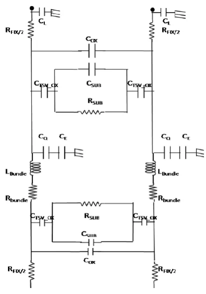
[image:3.595.322.529.49.343.2]During the recent past years, several researchers have designed a way to stack ICs more compactly in order to achieve `More than Moore‟ [22, 23]. In such organization, IC layers were stacked on top of each other in order to integrate more number of devices on a single chip which gave improved performance. This implemented technique is known as 3-D die stacking [24, 25]. Various advantages of this 3-D technology include higher transistor density, improved speed, lower power dissipation and area [26]. To achieve this type of arrangement a TSV model has been proposed in order to simplify the ESC model.
Figure 4. TSV model for GNR
CTSV-ox is the oxide capacitance around the via [18]. Cox is the oxide capacitance around two TSV [25, 27]. These two capacitances depend upon the thickness of SiO2 layer (tox) and are given by
CTSV −OX =4𝜀0𝜀𝑟𝑡𝑠𝑖
𝑤𝑇𝑆𝑉−𝑡𝑜𝑥
𝑡𝑜𝑥 (13) Cox= 𝐶 2
𝑇𝑆𝑉 −𝑜𝑥 +
𝜀0𝜀𝑟𝐴
𝑑𝑝𝑖𝑡𝑐 ℎ
−1 −1
(14)
where A = HTSV× wTSV, dpitch= w + s,
w is the width of TSV, s is the spacing between two TSVs, HTSV = height of TSV, ε0 is the permittivity of vaccum and εr is permittivity of SiO2.
The conductance and capacitance of silicon substrate are given by [18],
𝐺𝑆𝑈𝐵= 𝜎𝜋
ln [𝑑𝑝𝑖𝑡𝑐 ℎ
𝑤 𝑇𝑆𝑉+ ( 𝑑𝑝𝑖𝑡𝑐 ℎ
𝑤 𝑇𝑆𝑉)2−1]
(15)
CSUB =𝜀0𝜀𝑟𝐴
𝑑𝑝𝑖𝑡𝑐 ℎ (16) Where ζ = 0.1 𝛺. 𝑐𝑚 −1 is the conductivity of silicon
substrate [18].
F. Quantum and intrinsic resistance (𝑅𝑞′)
𝑅𝑞′= ℎ
2𝑒2𝑁𝑇𝑂𝑇𝐴𝐿 (17) Scattering resistance exists due to higher nanotube length that exceeds mean free path of electrons. Due to this electrons suffer scattering and thus are scattered in a different directions [18].
𝑅𝑆= ℎ
2𝑒2×𝑁𝐿𝐴𝑌𝐸𝑅 × (
1 𝜆𝑒𝑓𝑓 _𝑛)
−1−1
𝑛 (18) G. Quantum (CQ’) and Electrostatic capacitance (𝐶𝑒)
Quantum capacitance in GNR represents the finite density of states at Fermi energy. It depends on the number of conducting channel and number of layers of GNR [12].
𝐶𝑄′= 𝐶𝑄× 𝑁𝑇𝑂𝑇𝐴𝐿 (19)
Electrostatic capacitances exists due to the potential difference between the GNR bundle and ground plane. It depends on the width of GNR and distance between GNR bundle and the ground [12].
𝐶𝑒=
𝜀𝑤
𝑑 (20) H. Kinetic and magnetic inductances
Kinetic inductance originates from kinetic energy of electrons. It depends upon the length of GNR and increases with increase in its length. Magnetic inductance arises due to magnetic field induced by current flowing through a nanotube [8].
𝐿𝐾′= ℎ
4𝑒2𝑁
𝐶𝐻𝜗𝑓 (21) IV. SIMULATION SETUP
This research paper analyzes the propagation delay for MLGNRs, and MWCNT bundle at various technology nodes at varying interconnect lengths ranging from 400μm to 2000 μm. DIL system with CMOS driver is used at 32nm technology node. The interconnect line of DIL system is terminated with a load capacitance CL = 10af with supply voltage Vdd =1V for accurate estimation of delay and crosstalk. The ESC models of MLGNR and MWCNT bundle are replace with the interconnect line [28].
Fig.5. Driver Interconnect Load (DIL) System.
V. RESULTS AND DISCUSSION
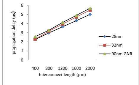
HSPICE simulations are performed for MLGNRs and MWCNTs bundle structures to address the propagation
delay of different structures. The propagation delay increases with interconnect lengths but reduces at lower technology node. The reason behind that the propagation delay primarily depends on interconnect parasitic such as resistance, capacitance and inductance. The increasing number of shells in MWCNT increases the number of conducting channel due to that reduces the interconnect parasitics resistance and inductance results decreases the propagation delay.
Finally, the propagation delay for different bundle arrangements is summarized in Table 1. It has been observed that propagation delay significantly reduces for lower technology node.
[image:4.595.313.548.209.352.2]Figure 6. Propagation delays for MLGNRs structure at different technology node.
[image:4.595.312.546.390.542.2]Figure 7. Propagation delays for MWCNT bundle structure at different technology node.
Table 1. Propagation Delay For MLGNR and MWCN bundle at different technology node.
28nm 32nm 90nm
Interco nnect length (in μm)
GNR MWC
- -NT
GNR
MW--CNT GN R
MW--CNT
400 2.25 3.56 2.28 3.58 2.56 3.78 800 2.97 5.52 3.16 5.65 3.26 5.81 1200 3.65 7.46 3.94 7.66 4.12 7.89 1600 4.31 9.43 4.71 9.63 4.89 9.91 2000 5.00 11.40 5.48 11.86 5.54 12.12
0 1 2 3 4 5 6
400 800 1200 1600 2000
p
rop
ag
atio
n
d
elay
(ns
)
Interconnect length (µm)
28nm
32nm
90nm GNR
0 2 4 6 8 10 12 14
400 800 1200 1600 2000
p
rop
ag
atio
n
d
elay
(ns
)
Interconnect length (µm)
VI. CONCLUSION
This paper introduces a MLGNRs and MWCNT bundle structure at different technology node and presented the ESC model for MLGNR and MWCNT bundle structure. Propagation delay has been analyzed for bundle structures at different global interconnect lengths. It has been observed that the propagation delay primarily depends on interconnect parasitic that is basically depends on the number of CNT presents in the bundle or on total number of conducting channel. On an average, the propagation delay are improved at lower technology node, the overall delays are reduced by 6.311% and 10.86% respectively for MWCT bundle and MLGNR compared to higher technology node.
REFERENCES
[1] Reddy, K.N. Majumdar, M.K. Kaushik, B.K., Anand, B., & Das, P. K.”Optimized delay and power performances in multilayer graphene nanoribbon interconnects”, Asia Pacific Conference on Postgraduate
Research In Microelectronics and Electronics 2012, pp. 122-125.
[2] Pieters, P., &Beyne, E “ 3D wafer level packaging approach towards cost effective low loss high density 3D stacking in Electronic
Packaging Technology, 2006.ICEPT'06, pp. 1-4.
[3] Behnam, A., Lyons, A. S., Bae, M. H., Chow, E. K., Islam, S., Neumann, C. M., & Pop, E. (2012), “Transport in nanoribbon interconnects obtained from graphene grown by chemical vapor deposition”. Nano letters, 12(9), 4424-4430.
[4] Lo, W. C., Chang, S. M., Chen, Y. H., Ko, J. D., Kuo, T. Y., Chang, H. H., & Shih, Y. C. (2007, April). 3D chip-to-chip stacking with through silicon interconnects. In VLSI Technology, Systems and
Applications, 2007.VLSI-TSA 2007.International Symposium on pp.
1-2.
[5] Kannan, S., Gupta, A., Kim, B. C., Mohammed, F., &Ahn, B. (2010, June). Analysis of carbon nanotube based through silicon vias.
In 2010 Proceedings 60th Electronic Components and Technology
Conference (ECTC).
[6] Hall, S. H., & Heck, H. L. (2011) “Advanced signal integrity for high-speed digital designs” John Wiley & Sons.
[7] Sarkar, D., Xu, C., Li, H., & Banerjee, K. (2011). High-frequency behavior of graphene-based interconnects—Part I: Impedance modeling. Electron Devices, IEEE Transactions on, 58(3), 843-852. [8] Cui, J. P., Zhao, W. S., Yin, W. Y., & Hu, J. (2012) “Signal
transmission analysis of multilayer graphe nenano-ribbon (MLGNR) interconnects” Electromagnetic Compatibility, IEEE Transactions 54(1), 126-132.
[9] Sarto, M. S., & Tamburrano, A. “Single-conductor transmission-line model of multiwall carbon nanotubes”. Nanotechnology, IEEE Transactions on, 9(1), 82-92, 2010.
[10] Zhao, W. S., Yin, W. Y., & Guo, Y. X. (2012) “Electromagnetic compatibility-oriented study on through silicon single-walled carbon nanotube bundle via (TS-SWCNTBV) arrays” Electromagnetic
Compatibility, IEEE Transactions on, 54(1), 149-157.
[11] Nasiri, S. H., Faez, R., & Moravvej-Farshi, M. K. (2012). Compact formulae for number of conduction channels in various types of graphene nanoribbons at various temperatures. Modern Physics Letters B, 26(01), 1150004.
[12] M. S. Sarto and A. Tamburrano, "Comparative analysis of TL models for multilayer graphene nanoribbon and multiwall carbon nanotube interconnects," Electromagnetic Compatibility (EMC), 2010 IEEE
International Symposium on, Fort Lauderdale, FL, 2010.
[13] Awano, Y. (2006) “Carbon nanotube technologies for LSI via interconnects” IEEE transactions on electronics, 89(11), 1499-1503. [14] Radosavljević, M., Lefebvre, J., & Johnson, A. T. (2001) “High-field
electrical transport and breakdown in bundles of single-wall carbon nanotubes” Physical Review B, 64(24), 241307.
[15] Wei, B. Q., Vajtai, R., &Ajayan, P. M. (2001) “Reliability and current carrying capacity of carbon nanotubes” Applied Physics Letters, 79(8), 1172-1174.
[16] Strano, M. S., Dyke, C. A., Usrey, M. L., Barone, P. W., Allen, M. J., Shan, H., & Smalley, R. E. (2003) “Electronic structure control of single-walled carbon nanotube functionalization” Science, 301(5639), 1519-1522.
[17] Engin, A. E., & Narasimhan, S. R. (2013) “Modeling of crosstalk in through silicon vias” Electromagnetic Compatibility, IEEE Transactions on, 55(1), 149-158.
[18] Majumder, M. K., Kumari, A., Kaushik, B. K., & Manhas, S. K. (2014) “Signal Integrity Analysis in Carbon Nanotube Based Through-Silicon Via” Active and Passive Electronic Components, 2014.
[19] Bolotin, K. I., Sikes, K. J., Hone, J., Stormer, H. L., & Kim, P. (2008) “Temperature-dependent transport in suspended graphene” Physical review letters, 101(9), 096802.
[20] Majumder, M. K., Das, P. K., & Kaushik, B. K. (2014) “Delay and crosstalk reliability issues in mixed MWCNT bundle interconnects” Microelectronics Reliability, 54(11), 2570-2577. [21] Zhao, W. S., & Yin, W. Y. (2014) “Comparative study on multilayer
graphene nanoribbon (MLGNR) interconnects” Electromagnetic
Compatibility, IEEE Transactions on, 56(3), 638-645.
[22] Kumar, V. R., Kaushik, B. K., & Majumder, M. K. (2014) “Graphene Based On-Chip Interconnects and TSVs: Prospects and Challenges”
Nanotechnology Magazine, IEEE, 8(4), 14-20.
[23] Kim, J., Pak, J. S., Cho, J., Song, E., Cho, J., Kim, H., & Yang, S. (2011) “ High-frequency scalable electrical model and analysis of a through silicon via (TSV)” Components, Packaging and
Manufacturing Technology, IEEE Transactions on, 1(2), 181-195.
[24] Awano, Y. (2009) “Graphene for VLSI” In 2009 International
Electron Devices Meeting, IEDM 2009.
[25] Xu, C., Li, H., Suaya, R., & Banerjee, K. (2010) “Compact AC modeling and performance analysis of through-silicon vias in 3-D ICs” Electron Devices, IEEE Transactions on, 57(12), 3405-3417. [26] Li, H., Lu, W. G., Li, J. J., Bai, X. D., &Gu, C. Z. (2005)
“Multichannel ballistic transport in multiwall carbon nanotubes” Physical review letters,95(8), 086601.
[27] Xu, C., Li, H., & Banerjee, K. (2008, December) “Graphene nano-ribbon (GNR) interconnects: A genuine contender or a delusive dream?”. In Electron Devices Meeting
[28] Xu, C., Li, H., & Banerjee, K. (2009) “Modeling, analysis, and design of graphene nano-ribbon interconnects” Electron Devices, IEEE Transactions on, 56(8), 1567-1578.
[29] P. R. Wallace, “The Band Theory of Graphite,” Physical Review, Vol. 71, No. 9, 1947, pp. 622-634. doi:10.1103/PhysRev.71.622. [30] Areshkin, D. A., Gunlycke, D., & White, C. T. (2007) “Ballistic
![figure. 1. The distance between the ground plane and GNR Geometry of MLGNR above ground plane is shown in layer is denoted by„d‟ where d= 50nm [8]](https://thumb-us.123doks.com/thumbv2/123dok_us/411867.538722/2.595.308.546.49.148/figure-distance-ground-plane-geometry-mlgnr-ground-denoted.webp)