Efficient BIST Hardware Insertion with Low Test Application Time for
Synthesized Data Paths
Nicola Nicolici and Bashir M. Al-Hashimi
School of Engineering and Advanced Technology, Staffordshire University
Stafford ST18 0AD, U.K.
Email:
[email protected]
Abstract
In this paper, new and efficient BIST methodology and BIST hardware insertion algorithms are presented for RTL data paths obtained from high level synthesis. The methodology is based on concurrent testing of modules with identical physical information by sharing the test pattern generators in a partial intrusion BIST environment. Furthermore, to reduce the number of signature analysis registers and test application time the same type modules are grouped in test compatibility classes and n-input k-bit comparators are used to check the results. The test application time is computed using an incremental test scheduling approach. An existing test scheduling algorithm is modified to obtain an efficient trade-off between the algorithm complexity and testable design space exploration. A cost function based on both test application time and area overhead is defined and a tabu search-based heuristic capable of exploring the solution space in a very rapid time is presented. To reduce the computational time testable design space exploration is carried out in two phases: test application time reduction phase and BIST area reduction phase. Experimental results are included confirming the efficiency of the proposed methodology.
1.
Introduction
Built-in self-test BIST is a design-for-testability (DFT) technique in which testing is accomplished through built-in hardware [1]. Pseudo-random BIST techniques use linear feedback shift registers (LFSRs) to perform test pattern generation (PG), whilst multiple-input signature registers (MISRs) carry out signature analysis (SA). Built-in logic block observation (BILBO) registers [2] are used
to perform either PG or SA, and concurrent BILBOs (CBILBOs) perform PG and SA simultaneously. Today’s need for a shorter time to market makes manual insertion of BIST circuitry an unaffordable design bottleneck and synthesis-based approaches were adopted.
complexity than RTL descriptions. The suboptimal test hardware insertion caused by the low complexity of RTL descriptions can be overcome by the fact that same type modules share the same physical information which is the focus of this paper. Furthermore the sharing of test pattern generators and reuse of signature analysis registers, as presented in our paper, can also solve the problems of minimal test application time, low BIST area overhead and efficient test schedule at RTL.
2.
Preliminary definitions
A RTL data path consists of modules (functional resources), registers and multiplexers. Let nreg, nmod and
nres denote the number of registers, modules and
module-types. Portions of data path, such as multiplexers and registers, can easily be tested using functional patterns. The goal of partial intrusion BIST is to test all the modules using a subset of registers in the test mode. Any register that is connected to an input port of a module through only multiplexers can supply test patterns to that input port. The embeddings where both input ports of a module receive test patterns from the same test register are not valid in the proposed BIST methodology. The correlation between test patterns at the left and right input port would decrease the number of unique test patterns that could be applied, hence decreasing the fault coverage. Any register that collects data from the output port of a module through only multiplexers is a possible choice for modification as a BIST register to compress test responses. Because modules of the same type share the identical physical information a decrease in the test application time can be obtained by grouping modules of the same type into test compatibility classes (TCCs). A test compatibility class TCCi,j of a module type j is the set
of modules that can be tested at the same time under the current test register configuration. If a test register generates test patterns for the left input port of the functional module Mi and for the right input port of the
functional module Mj, it is considered a shared test
resource and modules Mi and Mj cannot belong to the
same test compatibility class. Similarly different-type modules cannot belong to the same test compatibility class due to the fact that their fault sets have different detection probability profiles. Each module-type j has
nclasses(j). All the modules from a TCCi,j receive the same
[image:2.595.312.539.273.400.2]test patterns. The output responses of all the modules from TCCi,j are compared by an n-input k-bit comparator,
where n is |TCCi,j| and k is the bit-width of the data path. If
two output signals differ, an error signal is activated to the BIST controller. If output responses of all the modules are the same, a single register compresses the responses in order to verify if this succession of output responses is the
correct one. Let ORS(Mk) denote the set of output registers
of module Mk. The output register set of a test
compatibility class ORS(TCCi,j) is the union of output
register sets of all the modules from TCCi,j. The register
that performs the signature analysis function for TCCi,j is
chosen from ORS(TCCi,j). Thus, instead of performing
compression of test responses for nmod modules, the test
response compression is performed for only
nresxQclasses(j) test compatibility classes. The n-input k-bit
comparator logic can be tested by a short deterministic
test set, in the same way as multiplexers. It should be noted when nmod = nres the proposed BIST methodology is
identical with the BIST embedding methodology [3,4,5] where each module is embedded between two test pattern generators and a signature analysis register.
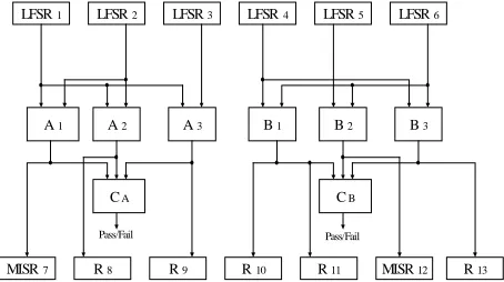
Figure 1. Data path example to illustrate the proposed BIST methodology
To illustrate the efficiency of RTL data path testing using TCCs consider the data path example of Figure 1, where LFSR1, LFSR2 and LFSR3 test three modules of
Atype, LFSR4, LFSR5 and LFSR6 test three modules of Btype.
LFSR1 generates test patterns for the left input port of A1,
A2 and A3. LFSR2 generates test patterns for the right input
port of A1 and A2, whilst LFSR3 provides test patterns for
the right input port of A3. Modules A1, A2 and A3 belong to
TCC0,0 (class index 0 and Atype index is 0). Similarly,
modules B1, B2 and B3 belong to TCC0,1 (class number 0
and Btype index is 1). Given the bit-width of the data path
as 8 bits, the output responses of the modules from TCC0,0
are compared by a 3-input 8-bit comparator (CA). Also,
the output responses of modules from TCC0,1 are
compared by another 3-input 8-bit comparator (CB). If any
error occurs during testing, the Pass/Fail signal will be activated and the testing process will stop. The ORS(A1) is
{R7}, the ORS(A2) is {R8}, and the ORS(A3) is {R9}.
Hence the ORS(TCC0,0) is {R7,R8,R9}. Any of these
registers can be configured as signature analysis register for TCC0,0. The procedure that chooses the optimal
signature analysis register is presented in section 4.2. For
LFSR 1 LFSR 2 LFSR 3 LFSR 4 LFSR 5 LFSR 6
A 1 A 2 A 3 B 1 B 2 B 3
C A C B
Pass/Fail Pass/Fail
data path example in Figure 1 the chosen register is R7.
Similarly, the ORS(TCC0,1) is {R10,R11,R12,R13} and the
chosen signature analysis register is R12.
3.
Local neighbourhood search of the
testable design space
Having defined the BIST methodology based on test compatibility classes the testable design space must be explored using an efficient BIST hardware insertion algorithm. The BIST hardware insertion algorithm looks for a testable solution with a primary goal of minimizing test application time and as a second order goal to minimize BIST hardware overhead. The testable design space exploration phases are detailed in section 5. This section focuses on the local neighbourhood of the testable design space and on generation of new neighbour solutions. In our problem formulation the current solution is a partially testable design where only the test pattern generators are allocated. The fully testable design is generated for each solution using the algorithms from section 4. The testable design space of partially testable designs is explored using a tabu search-based heuristic. Tabu search was proposed as a general combinatorial optimization technique [13]. This heuristic is similar to iterative improvement in that moves are sought which transform the current solution to its best neighbouring solution. The algorithm starts with an initial solution obtained by randomly assigning a single test pattern generator to every input port of every module from the RTL data path. Tabu search maintains a tabu list of its r most recent moves, with r circuit-dependent and varying from 5 (small designs) to 10 (complex designs). The tabu list exists to prevent cycling near a local minimum and also to enable uphill moves. In our problem formulation for a RTL data path with nreg registers there are nreg
neighbour solutions (one for each register from the data path). Each register Ri can generate test patterns to input
port IP of ni modules of module-type FRj. The neighbour
solution for register Ri is obtained by moving the test
pattern generation-function for input port IP of the ni
modules of module-type FRj modules to Ri and removing
the test pattern generator-function from registers that have previously generated test patterns for the respective ni
modules. When generating a neighbour solution for each register Ri there are a maximum of 2xnres potential moves
(one for each input port of every module-type for which the respective register can generate test patterns). To choose the best potential move to be evaluated by the tabu-search based algorithm two more metrics CSSD and
MSSD are introduced as follows.
The current spatial sharing degree CSSD(Ri, FRj, IP) of a
register Ri for a module-type FRj and input port IP is the
number of modules of the respective module-type which are fed by register Ri in the current testable solution. The
maximum spatial sharing degree MSSD(Ri, FRj, IP) of a
register Ri for a module-type FRj and input port IP is the
number of modules of the respective module-type which can be fed by the respective register using the data path interconnections. The metric which decides on the move for the respective register is ¨i(FRj, IP)= MSSD(Ri, FRj, IP)
- CSSD(Ri, FRj, IP). Having computed ¨i(FRj, IP) for each
module-type FRj, the transfer of test pattern
generation-functions for input port IP of module-type FRj to register
Ri is performed such that ¨i(FRj, IP) is maximal. If there
are two ore more input ports or module-types for which
[image:3.595.315.535.270.353.2]¨i is maximal then the decision is taken based on the maximum value of MSSD(Ri, FRj, IP).
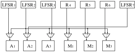
Figure 2. Partially specified testable design
In Figure 2 register R2 is configured as LFSR and
generates test vectors for the left input port of M1. It can
also generate test patterns for the left input port of A1 and
A2, the right input port of A3 and left input port of M2 and
M3. We compute ¨2(Atype,Left), ¨2(Atype,Right), and ¨2(Mtype,Left). Since R2 already performs pattern
generation for the left input port of Mtype we obtain ¨2(Mtype,Left)=3-1=2. In the same way ¨2(Atype
,Left)=2-0=2 and ¨2(Atype,Right)=1-0=1. Since ¨2(Mtype, Left)= ¨2(Atype,Left) and MSSD(R2,Mtype,Left)>MSSD(R2,Atype,Left),
the test pattern generation for Mtype is moved to R2 and the
area overhead is reduced because R5 and R6 do not
perform test pattern generation as shown in Figure 3.
Figure 3. Partially specified testable design after the move of test pattern generation functions to R2
L F S R 1 L F S R 2 L F S R 3 R 4 L F S R 5 L F S R 6
A 1 A 2 A 3 M 1 M 2 M 3
L F S R 7
L F S R 1 L F S R 2 L F S R 3 R 4 R 5 R 6
A 1 A 2 A 3 M 1 M 2 M 3
[image:3.595.313.530.569.657.2]4.
Incremental test scheduling algorithm
In the previous section we have described how partially specified testable designs are generated from one solution to another reducing test area overhead of test pattern generators. At this stage test compatibility classes are not complete. Many modules are not sharing test resources and they can be introduced in the already existing test compatibility classes. The test compatibility classes are completed such that the number of potential signature analysis registers is increased as described in subsection 4.1. Modules with different physical information will require different test times to satisfy required fault coverage. Thus, the incremental test scheduling problem will deal with unequal test lengths as described in subsection 4.2.
4.1 Generation of global test incompatibility
graph
In a partially specified testable solution all the modules are provided with their test pattern generators. Using the incompatibility between different modules in the partially specified testable design, an algorithm that guarantees the minimum number of test compatibility classes incompatible one with each other and an increase in the
ORS of each test compatibility class is described. The
creation of the global test incompatibility graph (G-TIG) where nodes are TCCs is done in three phases as follows.
In the first phase the test compatibility classes for each module-type are formed. If two modules of the same type share a test resource then an edge between the respective two modules is added in the local test incompatibility graph (L-TIG) of the respective module-type. The number of L-TIGs is nres. The L-TIGs are partitioned using an
efficient graph partitioning algorithm [7, algorithm 1]. In the second phase the sharing of test resources between modules of different module-types is examined. If Ma of
module-type m1 is incompatible with Mb of module-type
m2 and there is an edge in G-TIG between a TCCx,m1 and
TCCy,m2 then Ma is added to class x and Mb is added to
class y. Otherwise Ma is added class i such that:
ƒ(TCCi,m1,Ma)= |ORS(TCCi,m1 + Ma )|-|ORS(TCCi,m1 )|
is maximal and a new edge between TCCi,m1 and TCCy,m2,
where y is the class where Mb was assigned, is added to
G-TIG. Using this new measure (f) an increase in the
number of potential signature registers is assured. This increase will be used by the incremental test scheduling algorithm as outlined in the next subsection. In the third phase modules Ma of module-type m1 that are present in
[image:4.595.304.537.75.192.2]the data path but do not share any test registers are added to a test class i such that ƒ(TCCi,m1,Ma) is maximal.
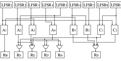
Figure 4. Data path example demonstrating the generation of G-TIG
Generation of G-TIG algorithm is illustrated by considering the data path in Figure 4. In the first step the
L-TIGs are created. Since modules that belong to Btype and
Ctype do not share test registers with same-type modules,
L-TIGs for these two module-types are void. Modules A1
and A2 cannot be tested at the same time because LFSR2 is
a shared test resource. Thus an incompatibility edge between A1 and A2 is introduced in the L-TIG of Atype.
Another edge added to the same L-TIG is between A2 and
A3 due to the sharing of test register LFSR2. So far, the test
classes for Atype are TCC0,0={A1, A3} and TCC1,0={A2} (0
is the index of Atype). In the second step TCC0,1 (1 is the
index of Btype) and TCC0,2 (2 is the index of Ctype) are
created. B1 and B2 are assigned to TCC0,1 whilst C1 and C2
are assigned to TCC0,2. Due to the sharing of LFSR3
between A3 and B1 an edge between TCC0,0 and TCC0,1 is
added. Similarly an edge between TCC0,0 and TCC0,2 is
added due to sharing of LFSR1 between A1 and C2. In the
third step, A4 is assigned to one of the TCCs of Atype. The
computed measures are ƒ(TCC0,0,A4)=1 and ƒ(TCC1,0,A4)=
2. We choose TCC1,0 due to higher increase in the size of
ORS. The test classes are TCC0,0={A1,A3}, TCC1,0={A2,
A4}, TCC0,1={B1,B2} and TCC0,2={C1,C2}.
4.2
Test scheduling and signature analysis
register allocation
The test scheduling algorithm for partitioned testing with run to completion reported in [7, algorithm 2M] is modified in order to schedule tests and allocate signature analysis registers simultaneously. If two test compatibility classes use the same signature register at different test times area overhead is reduced and the test control is simplified because the signature does not have to be shifted out. The concurrent test set (CTS) [7] contains the currently active tests. A similar data structure called busy register set (BRS) keeps the test registers that are currently performing signature analysis. When the shortest currently L F S R 1
A 1
L F S R 2 L F S R 3 L F S R 4 L F S R 5 L F S R 6 L F S R 7 L F S R 8 L F S R 9
A 2 A 3 A 4 B 1 B 2 C 1 C 2
active tests are completed and CTS is updated, the registers that performed signature analysis for the respective tests are removed from BRS. If TCCi,j is
compatible with all tests from CTS, but all the registers from ORS(TCCi,j) are present in BRS, then the test TCCi,j
is postponed until at least one register that can perform signature analysis for TCCi,j is removed from BRS. One
[image:5.595.322.516.80.259.2]more data structure, used register set (URS), stores the test registers that have already performed signature analysis at a previous test time. Choosing a register from URS to perform signature analysis for the currently scheduled test leads to a reduction in area overhead. Another reason for reusing the previous signature analysis registers is that the signature does not have to be shifted out, unless the test registers have to be configured at a later stage as test pattern generators. The increase in fault-escape probability caused by not shifting out the signatures after the completion of each test is compensated by the decrease in fault escape probability achieved by checking the output responses of modules from the same test compatibility class using the n-input k-bit comparators.
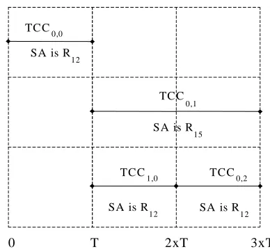
Figure 5. G-TIG for the data path example of Figure 4
To illustrate the above the G-TIG of the data path from Figure 4 is shown in Figure 5. It is assumed that the number of test patterns to test Atype and Ctype modules is
equal T0=T2=T, whilst the number of test patterns to test
Btype modules is double T1=2xT, with T a reasonable high
integer. The first test to be scheduled is TCC0,0 at test time
0. The signature analysis register is chosen from
ORS(TCC0,0) such that its fanin is maximum. We choose
R12 to perform the signature analysis for TCC0,0. At test
time T, the CTS is modified to reflect the removal of the
Figure 6. Test schedule for the data path example of Figure 4
completed test TCC0,0 and R12 is removed from BRS and
added to URS. At this point TCC0,1 is scheduled. The
register R15 is assigned to perform signature analysis for
TCC0,1. At the same time TCC1,0 is scheduled and register
R12 is considered for analyzing the responses of TCC1,0
because it is the only register from ORS(TCC1,0) that has
already been modified to a MISR (belongs to URS). An attempt to schedule TCC0,2 fails because both registers
that can perform signature analysis for this test class (R15
and R12) belong to BRS. The shortest currently active test
is completed at test time 2xT. Register R12 is removed
from BRS and another attempt to schedule TCC0,2 will
succeed because R12 will be available to perform signature
analysis. At test time 3xT all the currently active tests are completed. Note that only two test registers are required to perform signature analysis. A graphical representation of the test schedule is presented in Figure 6.
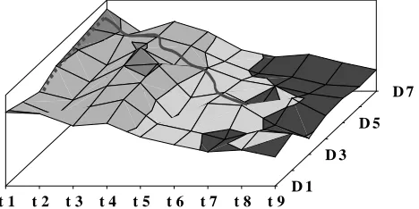
5. Testable design space exploration phases
In section 3 the local neighbourhood search of the testable design space was outlined. The test application time of the fully testable design computed using the incremental test scheduling algorithm given in section 4 is used to guide the testable design space exploration. Due to the topology of the testable design space and the local neighbourhood definition, in order to reach the best testable solution in low computational time the optimization is carried out in two phases. The need of this two-phase optimization process is justified by the three dimensional testable design space. There might be several testable designs with the same test application time but different BIST area overheads. Clearly in practice only the
TC C 0,0
TC C 0,1
TC C
1,0 TC C0,2
SA is R 12
SA is R 15
SA is R
12 SA is R12
0 T 2xT 3xT
T = 2xT ORS(TCC ) = {R , R , R , R }
0,0 10 12 13 14
ORS(TCC ) = {R , R , R , R }
ORS(TCC ) = {R }
ORS(TCC ) = {R , R }
1,0 11 12 13 14
0,1
0,2 15
15 12 TCC
0,0 TCC1,0
TCC
0,1 TCC0,2
T = T 0
T = T 0
1
[image:5.595.72.264.349.535.2]minimum test application time design with the smallest BIST area overhead is sought. Thus the primary goal is to minimize the test application time and the second order goal is to reduce the BIST area overhead. The BIST area overhead is computed in terms of the number of gates required to modify a register in a BIST register and the number of gates implementing n-input k-bit comparators. The testable design space is shown in Figure 7. Various testable designs (D1 to D7) with identical test application have different BIST area overheads. The best test application time testable design with minimum BIST area overhead is sought in this three dimensional testable design space.
Figure 7. Testable design space exploration
The two optimization phases are:
(i) Test application time reduction phase (ii) BIST area overhead reduction phase
In the first optimization phase the minimum test application time designs are sought. If two solutions have same test application time then the solution with higher area overhead is chosen. This is due to the topology of the testable design space where higher BIST area overhead testable designs can lead in fewer moves to a testable design with lower test application time. If any of the neighbour solutions has lower test application then it is accepted regardless of the BIST area overhead. In Figure 7 the test application time reduction phase is illustrated by the curve with a continuos line. Having reached the minimum test application time design in the first optimization phase, during the second optimization phase testable designs with lower BIST area overhead are sought. If two testable designs have the same test application then the testable design with lower BIST area overhead is chosen. If any of the testable designs has higher test application it is rejected regardless of the BIST area overhead. The curve with the dashed line in Figure 7 shows the BIST area overhead reduction phase. Using this two-phase optimization strategy the computational time required for testable design space exploration time is reduced as shown in the next section.
6. Experimental results
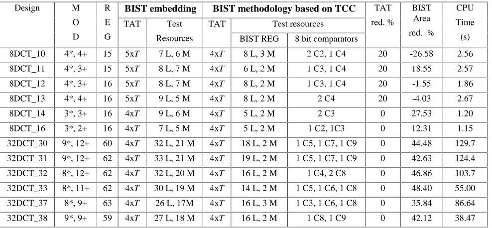
The proposed BIST hardware insertion algorithm based on TCCs has been implemented on SUN SPARC 20 workstation using 6000 lines of C++ code. Table 1 shows a comparison of experimental results in terms of test application time (TAT) and BIST area overhead obtained for the BIST embedding methodology and the proposed BIST methodology based on TCCs. The results for the BIST embedding methodology are obtained by considering nmod=nres. The RTL data paths are generated
using a high-level synthesis system [14]. The first column shows the design name and the execution time constraint which varies from 10 to 16 in the case of 8 point DCT and 30 to 38 in the case of 32 point DCT. The next two columns show the number of modules (MOD) in terms of multipliers (*) and adders (+) and the number of registers (REG) obtained from high level synthesis. The TAT for adders and multipliers was assumed T+=T and T*=4xT
with T a reasonable high integer. The first six rows show the experimental results for the 8 point DCT. In the first four rows the BIST embedding methodology produces testable data paths where TAT is not minimal. Applying the proposed BIST methodology based on TCCs, TAT is reduced by 20% from 5xT to 4xT. The reduction in TAT produces higher area overheads in some cases like 8DCT_10. However, the primary goal of reducing the TAT is achieved. Furthermore the number of BIST registers embedded in data path is reduced which leads to faster solutions. In the case of 8DCT_11, both TAT and BIST area overhead are reduced. The number of LFSRs (represented by L in Table 1) is reduced from 8 to 6 whilst the number of MISRs (represented by M in Table 1) is reduced from 7 to 2. In the proposed BIST methodology a single 3 input 8 bit comparator (C3) and a single 4 input 8 bit comparator (C4) are introduced. However these two comparators do not have high area overhead, reduce the fault escape probability and are easy testable. For the last two 8 point DCT designs the proposed BIST methodology reduces the BIST area overhead by 27% and 12% respectively which clearly outlines the efficiency of the second order BIST area optimization goal. The last 6 rows of Table 1 show that the proposed methodology is capable of dealing with complex DSP circuits such as 32 point DCT. Due to a very high number of registers the minimal TAT is achieved by both methodologies. The reductions in BIST area overhead are significant varying from 35% up to 48%. The algorithm has low computational time as shown in the last column of Table 1. For 8 point DCT the computational time varies from 1s to 3s. For 32 point DCT designs the computational time is still very low. The excellent computational time is achieved due to use of intelligent local neighbourhood search of the testable design space and the two-phase optimization strategy. t 1 t 2 t 3 t 4 t 5 t 6 t 7 t 8 t 9
D 1 D 3
7. Conclusions
New BIST methodology and BIST hardware insertion algorithms for synthesized data paths were presented. The methodology is based on grouping modules with same physical information in test compatibility classes. Input ports of compatible modules share test pattern generators in a partial intrusion BIST environment leading to savings in test application time. Module output responses from each test compatibility class are checked by an n-input
k-bit comparator leading to lower area overhead.
Near-optimal testable design is obtained in low computational time by a two-phase tabu search-based testable design space exploration.
References
[1] V.D., Agrawal, C.R., Kime, and K.K. Saluja. A tutorial on built-n self – part 1: Principles. IEEE Design & Test of
Computers, pp. 73-92, March 1993.
[2] V.D., Agrawal, C.R., Kime, and K.K. Saluja. A tutorial on built-in self test – part 2: Applications. IEEE Design & Test of
Computers, pp. 69-77, June 1993.
[3] P.R. Chalsani, S. Bhawmik, A. Acharya, and P. Palchaudhuri. Design of testable VLSI circuits with minimum area overhead. In IEEE Transactions on Computers, 38(9), pp. 1460-1462, 1989.
[4] A. Basu, T.C. Wilson, D.K. Banerji, and J.C. Majithia. An approach to minimize testability for BILBO based built-in self-test. In Proc. 5th Int. Conf on VLSI Design, pp. 354-355, 1992.
[5] S.P. Lin, C.A. Njinda, and M.A. Breuer. Generating a family of testable designs using the BILBO methodology. In Journal of
Electronic Testing: Theory and Applications (JETTA) 4, pp.
71-89, April 1993.
[6] C.I.H. Chen. Graph partitioning for concurrent test scheduling in VLSI circuits. In Proc. 28th Design Automation Conference, pp. 287-290, 1991.
[7] G.L. Craig, C.R. Kime, and K.K. Saluja. Test scheduling and control for VLSI built-in self-test. IEEE Transactions on
Computers, 37(9), pp.1099-1109, 1988.
[8] W.B. Jone, C.A. Papachristou, and M. Pereira. A scheme for overlaying concurrent testing of VLSI circuits. In Proc. 26th
Design Automation Conference, pp. 531-536, June 1989.
[9] A. Orailoglu., and I.G. Harris. Test path generation and test scheduling for self-testable designs. In Proc. International
Conference on Computer Design, pp. 528- 531, 1993.
[10] I.G. Harris, and A. Orailoglu. Fine-grained test concurrency in test scheduling for partial-intrusion BIST. In Proc. European
Design & Test Conference, pp. 119-123, 1994.
[11] S. Chiu, and C.A. Papachristou. A design for testability scheme with application to data path synthesis. In Proc.28th
Design Automation Conference, pp. 271-277, June 1991.
[12] A.P. Stroele, and H.J. Wunderlich. Hardware-optimal test register insertion. IEEE Transactions on Computer-Aided
Design of Integrated Circuits and Systems, 17(6), pp. 531-539,
1998.
[13] C.R. Reeves. Modern heuristic techniques for
combinatorial problems, McGraw-Hill Book Company, 1995.
[14]P. Kollig, and B.M. Al-Hashimi. Simultaneous scheduling, allocation and binding in high level synthesis. IEE Electronics
Letters, 33(18), pp. 1516-1518, 1997
BIST embedding BIST methodology based on TCC
Test resources
Design M
O
D R
E
G
TAT Test
Resources TAT
BIST REG 8 bit comparators
TAT
red. %
BIST Area
red. %
CPU
Time
(s)
8DCT_10 4*, 4+ 15 5xT 7 L, 6 M 4xT 8 L, 3 M 2 C2, 1 C4 20 -26.58 2.56
8DCT_11 4*, 3+ 15 5xT 8 L, 7 M 4xT 6 L, 2 M 1 C3, 1 C4 20 18.55 2.57
8DCT_12 4*, 3+ 16 5xT 8 L, 7 M 4xT 8 L, 2 M 1 C3, 1 C4 20 -1.55 1.86
8DCT_13 4*, 4+ 16 5xT 9 L, 5 M 4xT 8 L, 2 M 2 C4 20 -4.03 2.67
8DCT_14 3*, 3+ 16 4xT 9 L, 6 M 4xT 5 L, 2 M 2 C3 0 27.53 1.20
8DCT_16 3*, 2+ 16 4xT 7 L, 5 M 4xT 5 L, 2 M 1 C2, 1C3 0 12.31 1.15
32DCT_30 9*, 12+ 60 4xT 32 L, 21 M 4xT 18 L, 2 M 1 C5, 1 C7, 1 C9 0 44.48 129.7
32DCT_31 9*, 12+ 62 4xT 33 L, 21 M 4xT 19 L, 2 M 1 C5, 1 C7, 1 C9 0 42.63 124.4
32DCT_32 8*, 12+ 62 4xT 32 L, 20 M 4xT 16 L, 2 M 1 C4, 2 C8 0 46.86 103.7
32DCT_33 8*, 11+ 62 4xT 30 L, 19 M 4xT 14 L, 2 M 1 C5, 1 C6, 1 C8 0 48.40 55.00
32DCT_37 8*, 9+ 63 4xT 26 L, 17M 4xT 16 L, 3 M 1 C3, 1 C6, 1 C8 0 35.84 86.64
[image:7.595.52.546.76.305.2]32DCT_38 9*, 9+ 59 4xT 27 L, 18 M 4xT 16 L, 2 M 1 C8, 1 C9 0 42.12 38.47