MOTOROLA.COM/SEMICONDUCTORS
HCS12
Microcontrollers
"CONTROLLED COPY"
S12MMCV4/D Rev. 4.00
Module Mapping
Control (MMC) V4
PRINTED VERSIONS ARE UNCONTROLLED EXCEPT WHEN STAMPED
"CONTROLLED COPY"
IN RED
Block Guide — S12MMC V4
2
Motorola and the Stylized M Logo are registered trademarks of Motorola, Inc. DigitalDNA is a trademark of Motorola, Inc.
This product incorporates SuperFlash® technology licensed from SST. © Motorola, Inc., 2003
Revision History
Version Number
Revision Date
Effective
Date Author Description of Changes
4.00 2/4/2003 2/4/2003 John Langan
Creation of block user guide from core user guide version 1.5 (July 2, 2002). Changes include: updating format and making end customer friendly.
PRINTED VERSIONS ARE UNCONTROLLED EXCEPT WHEN STAMPED
"CONTROLLED COPY"
IN RED
Block Guide — S12MMC V4
4
List of Figures
Figure 1-1 Module Mapping Control Block Diagram . . . 5
Figure 3-1 Module Mapping Control Register Summary. . . 9
Figure 3-2 Initialization of Internal RAM Position Register (INITRM) . . . 10
Figure 3-3 Initialization of Internal Registers Position Register (INITRG) . . . 10
Figure 3-4 Initialization of Internal EEPROM Position Register (INITEE) . . . 11
Figure 3-5 Miscellaneous System Control Register (MISC) . . . 12
Figure 3-6 Reserved Test Register Zero (MTST0) . . . 13
Figure 3-7 Reserved Test Register One (MTST1) . . . 13
Figure 3-8 Memory Size Register Zero . . . 14
Figure 3-9 Memory Size Register One . . . 15
Figure 3-10 Program Page Index Register (PPAGE) . . . 16
Figure 4-1 Memory Paging Example: 1M Byte On-Chip FLASH/ROM, 64K Allocation . . . 25
List of Tables
Table 3-1 External Stretch Bit Definition . . . 12Table 3-2 Allocated EEPROM Memory Space . . . 14
Table 3-3 Allocated RAM Memory Space . . . 15
Table 3-4 Allocated FLASH/ROM Physical Memory Space . . . 16
Table 3-5 Allocated Off-Chip Memory Options . . . 16
Table 3-6 Program Page Index Register Bits . . . 17
Table 4-1 Select Signal Priority . . . 19
Table 4-2 Allocated Off-Chip Memory Options . . . 21
Table 4-3 External/Internal Page Window Access. . . 21
Table 4-4 0K Byte Physical FLASH/ROM Allocated . . . 23
Table 4-5 16K Byte Physical FLASH/ROM Allocated . . . 23
Table 4-6 48K Byte Physical FLASH/ROM Allocated . . . 23
Table 4-7 64K Byte Physical FLASH/ROM Allocated . . . 24
"CONTROLLED COPY"
IN RED
1.1 Overview. . . 2
1.2 Features . . . 2
1.3 Modes of Operation . . . 2
Section 2 External Signal Description
Section 3 Memory Map/Register Definition
3.1 Register Descriptions . . . 63.1.1 Initialization of Internal RAM Position Register (INITRM) . . . 6
3.1.2 Initialization of Internal Registers Position Register (INITRG) . . . 6
3.1.3 Initialization of Internal EEPROM Position Register (INITEE) . . . 7
3.1.4 Miscellaneous System Control Register (MISC) . . . 8
3.1.5 Reserved Test Register Zero (MTST0) . . . 9
3.1.6 Reserved Test Register One (MTST1) . . . 9
3.1.7 Memory Size Register Zero (MEMSIZ0) . . . 10
3.1.8 Memory Size Register One (MEMSIZ1). . . 11
3.1.9 Program Page Index Register (PPAGE) . . . 12
Section 4 Functional Description
4.1 Bus Control. . . 154.2 Address Decoding . . . 15
4.2.1 Select Priority and Mode Considerations . . . 15
4.2.2 Emulation Chip Select Signal. . . 16
4.2.3 External Chip Select Signal . . . 16
4.3 Memory Expansion. . . 16
4.3.1 CALL and Return from Call Instructions. . . 18
PRINTED VERSIONS ARE UNCONTROLLED EXCEPT WHEN STAMPED "CONTROLLED COPY" IN RED
Block Guide — S12MMC V4
"CONTROLLED COPY"
IN RED
Section 1 Introduction to Module Mapping Control (MMC)
This section describes the functionality of the Module Mapping Control (MMC) sub-block of the S12 Core Platform.
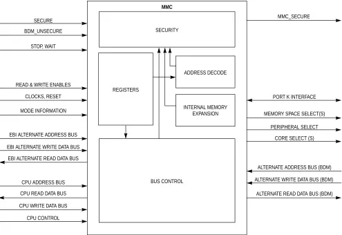
[image:7.612.60.555.167.507.2]The block diagram of the MMC is shown inFigure 1-1.
Figure 1-1 Module Mapping Control Block Diagram
MMC
MODE INFORMATION
REGISTERS
CPU WRITE DATA BUS CPU ADDRESS BUS
CPU CONTROL STOP, WAIT
ADDRESS DECODE
CPU READ DATA BUS EBI ALTERNATE ADDRESS BUS
EBI ALTERNATE WRITE DATA BUS
EBI ALTERNATE READ DATA BUS
SECURITY
CLOCKS, RESET READ & WRITE ENABLES
ALTERNATE ADDRESS BUS (BDM)
ALTERNATE WRITE DATA BUS (BDM)
ALTERNATE READ DATA BUS (BDM) CORE SELECT (S) PORT K INTERFACE
MEMORY SPACE SELECT(S)
PERIPHERAL SELECT
BUS CONTROL SECURE
BDM_UNSECURE
MMC_SECURE
PRINTED VERSIONS ARE UNCONTROLLED EXCEPT WHEN STAMPED
"CONTROLLED COPY"
IN RED
Block Guide — S12MMC V4
2
1.1 Overview
The MMC is the submodule which controls memory map assignment and selection of internal resources and external space. Internal buses between the core and memories and between the core and peripherals is controlled in this module. The memory expansion is generated in this module.
1.2 Features
• Registers for mapping of address space for on-chip RAM, EEPROM, and FLASH (or ROM) memory blocks and associated registers
• Memory mapping control and selection based upon address decode and system operating mode
• Core address bus control
• Core data bus control and multiplexing
• Core security state decoding
• Emulation chip select signal generation (ECS)
• External chip select signal generation (XCS)
• Internal memory expansion
• External stretch and ROM mapping control functions via the MISC register
• Reserved registers for test purposes
• Configurable system memory options defined at integration of Core into the System-on-a-Chip (SOC).
1.3 Modes of Operation
"CONTROLLED COPY"
IN RED
Section 2 External Signal Description
PRINTED VERSIONS ARE UNCONTROLLED EXCEPT WHEN STAMPED "CONTROLLED COPY" IN RED
Block Guide — S12MMC V4
"CONTROLLED COPY"
IN RED
Section 3 Memory Map/Register Definition
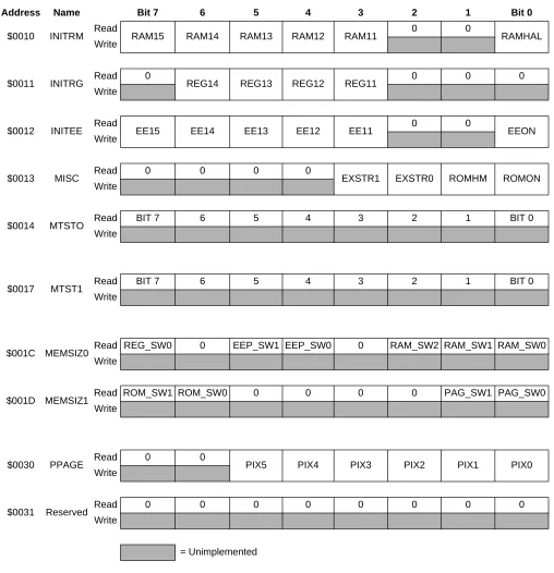
[image:11.612.55.563.137.663.2]A summary of the registers associated with the MMC sub-block is shown inFigure 3-1. Detailed descriptions of the registers and bits are given in the subsections that follow.
Figure 3-1 Module Mapping Control Register Summary
Address Name Bit 7 6 5 4 3 2 1 Bit 0
$0010 INITRM Read RAM15 RAM14 RAM13 RAM12 RAM11 0 0 RAMHAL
Write
$0011 INITRG Read 0 REG14 REG13 REG12 REG11 0 0 0
Write
$0012 INITEE Read EE15 EE14 EE13 EE12 EE11 0 0 EEON
Write
$0013 MISC Read 0 0 0 0 EXSTR1 EXSTR0 ROMHM ROMON
Write
$0014 MTSTO Read BIT 7 6 5 4 3 2 1 BIT 0
Write
$0017 MTST1 Read BIT 7 6 5 4 3 2 1 BIT 0
Write
$001C MEMSIZ0 Read REG_SW0 0 EEP_SW1 EEP_SW0 0 RAM_SW2 RAM_SW1 RAM_SW0
Write
$001D MEMSIZ1 Read ROM_SW1 ROM_SW0 0 0 0 0 PAG_SW1 PAG_SW0
Write
$0030 PPAGE Read 0 0 PIX5 PIX4 PIX3 PIX2 PIX1 PIX0
Write
$0031 Reserved Read 0 0 0 0 0 0 0 0
Write
PRINTED VERSIONS ARE UNCONTROLLED EXCEPT WHEN STAMPED
"CONTROLLED COPY"
IN RED
Block Guide — S12MMC V4
6
3.1 Register Descriptions
[image:12.612.95.526.126.207.2]3.1.1 Initialization of Internal RAM Position Register (INITRM)
Figure 3-2 Initialization of Internal RAM Position Register (INITRM)
Read: Anytime
Write: Once in Normal and Emulation Modes, anytime in Special Modes
NOTE: Writes to this register take one cycle to go into effect.
This register initializes the position of the internal RAM within the on-chip system memory map.
RAM15–RAM11 — Internal RAM Map Position
These bits determine the upper five bits of the base address for the system’s internal RAM array.
RAMHAL — RAM High-Align
RAMHAL specifies the alignment of the internal RAM array.
0 = Aligns the RAM to the lowest address ($0000) of the mappable space 1 = Aligns the RAM to the higher address ($FFFF) of the mappable space
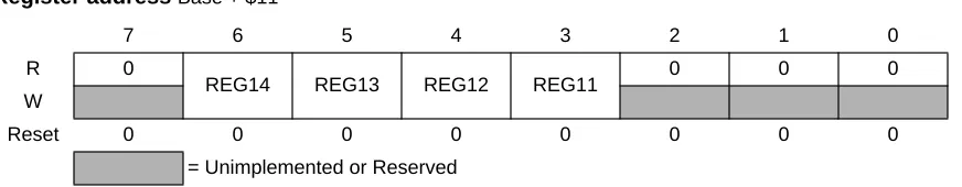
3.1.2 Initialization of Internal Registers Position Register (INITRG)
Figure 3-3 Initialization of Internal Registers Position Register (INITRG)
Read: Anytime
Write: Once in Normal and Emulation modes and anytime in Special modes Register addressBase + $10
7 6 5 4 3 2 1 0
R
RAM15 RAM14 RAM13 RAM12 RAM11 0 0 RAMHAL
W
Reset 0 0 0 0 1 0 0 1
= Unimplemented or Reserved
Register addressBase + $11
7 6 5 4 3 2 1 0
R 0
REG14 REG13 REG12 REG11 0 0 0
W
Reset 0 0 0 0 0 0 0 0
[image:12.612.93.529.503.588.2]"CONTROLLED COPY"
IN RED
This register initializes the position of the internal registers within the on-chip system memory map. The registers occupy either a 1K byte or 2K byte space and can be mapped to any 2K byte space within the first 32K bytes of the system’s address space.
REG14–REG11 — Internal Register Map Position
These four bits in combination with the leading zero supplied by bit 7 of INITRG determine the upper five bits of the base address for the system’s internal registers (i.e., the minimum base address is $0000 and the maximum is $7FFF).
[image:13.612.88.533.217.296.2]3.1.3 Initialization of Internal EEPROM Position Register (INITEE)
Figure 3-4 Initialization of Internal EEPROM Position Register (INITEE)
Read: Anytime
Write: The EEON bit can be written to any time on all devices. Bits E11–E15 are "Write anytime in all modes" on most devices. On some devices, bits E11–E15 are "Write once in Normal and Emulation modes and write anytime in Special modes". See device User’s Guide to determine the actual write access rights.
NOTE: Writes to this register take one cycle to go into effect.
This register initializes the position of the internal EEPROM within the on-chip system memory map.
EE15–EE11 — Internal EEPROM Map Position
These bits determine the upper five bits of the base address for the system’s internal EEPROM array.
EEON — Enable EEPROM
This bit is used to enable the EEPROM memory in the memory map.
1 = Enables the EEPROM in the memory map at the address selected by EE15–EE11. 0 = Disables the EEPROM from the memory map.
Register addressBase + $12
7 6 5 4 3 2 1 0
R
EE15 EE14 EE13 EE12 EE11 0 0 EEON
W Reset(1)
NOTES:
1. The reset state of this register is controlled at chip integration. Please refer to the specific device User’s Guide to determine the actual reset state of this register.
— — — — — — — —
PRINTED VERSIONS ARE UNCONTROLLED EXCEPT WHEN STAMPED
"CONTROLLED COPY"
IN RED
Block Guide — S12MMC V4
8
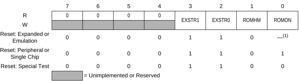
[image:14.612.68.549.97.228.2]3.1.4 Miscellaneous System Control Register (MISC)
Figure 3-5 Miscellaneous System Control Register (MISC)
Read: Anytime
Write: As stated in each bit description
NOTE: Writes to this register take one cycle to go into effect
This register initializes miscellaneous control functions.
EXSTR1 and EXSTR0 — External Access Stretch Bits 1 and 0
Write: Once in Normal and Emulation modes and anytime in Special modes
This two bit field determines the amount of clock stretch on accesses to the external address space as shown inTable 3-1. In single chip and peripheral modes these bits have no meaning or effect.
ROMHM — FLASH EEPROM or ROM Only in Second Half of Memory Map
Write: Once in Normal and Emulation modes and anytime in Special modes
1 = Disables direct access to the FLASH EEPROM or ROM in the lower half of the memory map. These physical locations of the FLASH EEPROM or ROM can still be accessed through the Program Page window.
0 = The fixed page(s) of FLASH EEPROM or ROM in the lower half of the memory map can be accessed.
Register addressBase + $13
7 6 5 4 3 2 1 0
R 0 0 0 0
EXSTR1 EXSTR0 ROMHM ROMON
W
Reset: Expanded or
Emulation 0 0 0 0 1 1 0 —
(1)
NOTES:
1. The reset state of this bit is determined at the chip integration level. Reset: Peripheral or
Single Chip 0 0 0 0 1 1 0 1
Reset: Special Test 0 0 0 0 1 1 0 0
= Unimplemented or Reserved
Table 3-1 External Stretch Bit Definition
Stretch Bit EXSTR1
Stretch Bit EXSTR0
Number of E Clocks Stretched
0 0 0
0 1 1
1 0 2
[image:14.612.122.489.485.580.2]"CONTROLLED COPY"
IN RED
ROMON — Enable FLASH EEPROM or ROM
Write: Once in Normal and Emulation modes and anytime in Special modes
This bit is used to enable the FLASH EEPROM or ROM memory in the memory map. 1 = Enables the FLASH EEPROM or ROM in the memory map.
0 = Disables the FLASH EEPROM or ROM from the memory map.
[image:15.612.92.524.187.267.2]3.1.5 Reserved Test Register Zero (MTST0)
Figure 3-6 Reserved Test Register Zero (MTST0)
Read: Anytime
Write: No effect — this register location is used for internal test purposes.
3.1.6 Reserved Test Register One (MTST1)
Figure 3-7 Reserved Test Register One (MTST1)
Read: Anytime
Write: No effect — this register location is used for internal test purposes. Register addressBase + $14
7 6 5 4 3 2 1 0
R 0 0 0 0 0 0 0 0
W
Reset 0 0 0 0 0 0 0 0
= Unimplemented or Reserved
Register addressBase + $17
7 6 5 4 3 2 1 0
R 0 0 0 0 0 0 0 0
W
Reset 0 0 0 1 0 0 0 0
[image:15.612.95.524.403.483.2]PRINTED VERSIONS ARE UNCONTROLLED EXCEPT WHEN STAMPED
"CONTROLLED COPY"
IN RED
Block Guide — S12MMC V4
10
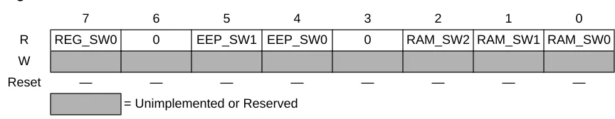
[image:16.612.91.523.94.178.2]3.1.7 Memory Size Register Zero (MEMSIZ0)
Figure 3-8 Memory Size Register Zero
Read: Anytime
Write: Writes have no effect
Reset: Defined at chip integration, see chip level documentation.
The MEMSIZ0 register reflects the state of the register, EEPROM and RAM memory space configuration switches at the Core boundary which are configured at system integration. This register allows read visibility to the state of these switches.
REG_SW0 — Allocated System Register Space
1 = Allocated system register space size is 2K byte 0 = Allocated system register space size is 1K byte
EEP_SW1:EEP_SW0 — Allocated System EEPROM Memory Space
The allocated system EEPROM memory space size is as given inTable 3-2. Register addressBase + $1C
7 6 5 4 3 2 1 0
R REG_SW0 0 EEP_SW1 EEP_SW0 0 RAM_SW2 RAM_SW1 RAM_SW0
W
Reset — — — — — — — —
= Unimplemented or Reserved
Table 3-2 Allocated EEPROM Memory Space
EEP_SW1:EEP_SW0 Allocated EEPROM Space
00 0K byte
01 2K bytes
10 4K bytes
"CONTROLLED COPY"
IN RED
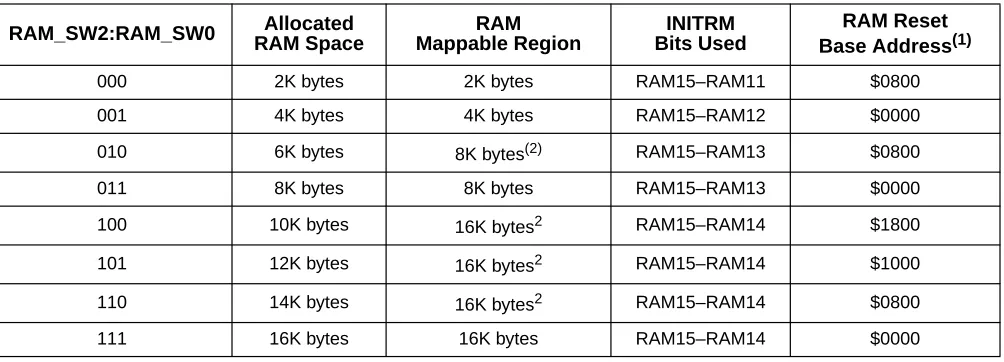
RAM_SW2:RAM_SW0 — Allocated System RAM Memory Space
The allocated system RAM memory space size is as given inTable 3-3.
NOTE: As stated, the bits in this register provide read visibility to the system physical memory space allocations defined at system integration. The actual array size for any given type of memory block may differ from the allocated size. Please refer to the chip-level documentation for actual sizes.
[image:17.612.58.560.114.295.2]3.1.8 Memory Size Register One (MEMSIZ1)
Figure 3-9 Memory Size Register One
Read: Anytime
Write: Writes have no effect
Reset: Defined at chip integration, see chip level documentation.
[image:17.612.90.527.455.544.2]The MEMSIZ1 register reflects the state of the FLASH or ROM physical memory space and paging switches at the Core boundary which are configured at system integration. This register allows read
Table 3-3 Allocated RAM Memory Space
RAM_SW2:RAM_SW0 Allocated RAM Space RAM Mappable Region INITRM Bits Used RAM Reset Base Address(1)
NOTES:
1. The RAM Reset BASE Address is based on the reset value of the INITRM register, $09.
000 2K bytes 2K bytes RAM15–RAM11 $0800
001 4K bytes 4K bytes RAM15–RAM12 $0000
010 6K bytes 8K bytes(2)
2. Alignment of the Allocated RAM space within the RAM mappable region is dependent on the value of RAMHAL.
RAM15–RAM13 $0800
011 8K bytes 8K bytes RAM15–RAM13 $0000
100 10K bytes 16K bytes2 RAM15–RAM14 $1800
101 12K bytes 16K bytes2 RAM15–RAM14 $1000
110 14K bytes 16K bytes2 RAM15–RAM14 $0800
111 16K bytes 16K bytes RAM15–RAM14 $0000
Register addressBase + $1D
7 6 5 4 3 2 1 0
R ROM_SW
1
ROM_SW
0 0 0 0 0 PAG_SW1 PAG_SW0
W
Reset — — — — — — — —
PRINTED VERSIONS ARE UNCONTROLLED EXCEPT WHEN STAMPED
"CONTROLLED COPY"
IN RED
Block Guide — S12MMC V4
12
ROM_SW1:ROM_SW0 — Allocated System FLASH or ROM Physical Memory Space
The allocated system FLASH or ROM physical memory space is as given inTable 3-4.
PAG_SW1:PAG_SW0 — Allocated Off-Chip FLASH or ROM Memory Space
The allocated off-chip FLASH or ROM memory space size is as given inTable 3-5.
NOTE: As stated, the bits in this register provide read visibility to the system memory space and on-chip/off-chip partitioning allocations defined at system integration. The actual array size for any given type of memory block may differ from the allocated size. Please refer to the chip-level documentation for actual sizes.
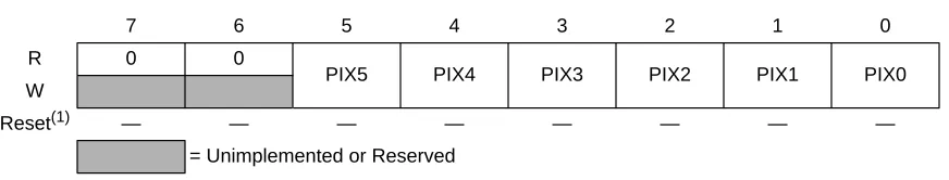
[image:18.612.118.485.105.247.2]3.1.9 Program Page Index Register (PPAGE)
Figure 3-10 Program Page Index Register (PPAGE) Table 3-4 Allocated FLASH/ROM Physical Memory Space
ROM_SW1:ROM_SW0 Allocated FLASHor ROM Space
00 0K byte
01 16K bytes
10 48K bytes(1)
11 64K bytes(1)
NOTES:
1. The ROMHM software bit in the MISC register determines the accessibility of the FLASH/ROM memory space. Please refer to 3.1.8 Memory Size Register One (MEMSIZ1) for a detailed functional description of the ROMHM bit.
Table 3-5 Allocated Off-Chip Memory Options
PAG_SW1:PAG_SW0 Off-Chip Space On-Chip Space
00 876K bytes 128K bytes
01 768K bytes 256K bytes
10 512K bytes 512K bytes
11 0K byte 1M byte
Register addressBase + $30
7 6 5 4 3 2 1 0
R 0 0
PIX5 PIX4 PIX3 PIX2 PIX1 PIX0
W Reset(1)
NOTES:
1. The reset state of this register is controlled at chip integration. Please refer to the specific device User’s Guide to determine the actual reset state of this register.
— — — — — — — —
[image:18.612.92.528.539.622.2]"CONTROLLED COPY"
IN RED
Read: Anytime
Write: Determined at chip integration. Generally it’s: “Write anytime in all modes”; on some devices it will be: “Write only in Special modes”. Check specific device documentation to determine which applies. Reset: Defined at chip integration as either $00 (paired with write in any mode) or $3C (paired with write only in special modes), see chip level documentation.
The HCS12 Core architecture limits the physical address space available to 64K bytes. The Program Page Index Register allows for integrating up to 1M byte of FLASH or ROM into the system by using the six page index bits to page 16K byte blocks into the Program Page Window located from $8000 to $BFFF as defined inTable 3-6. CALL and RTC instructions have special access to read and write this register without using the address bus.
NOTE: Normal writes to this register take one cycle to go into effect. Writes to this register using the special access of the CALL and RTC instructions will be complete before the end of the associated instruction.
PIX5–PIX0 — Program Page Index Bits 5–0
[image:19.612.125.487.330.568.2]These page index bits are used to select which of the 64 FLASH or ROM array pages is to be accessed in the Program Page Window as shown inTable 3-6.
Table 3-6 Program Page Index Register Bits
PIX5 PIX4 PIX3 PIX2 PIX1 PIX0 Program Space
Selected
0 0 0 0 0 0 16K page 0
0 0 0 0 0 1 16K page 1
0 0 0 0 1 0 16K page 2
0 0 0 0 1 1 16K page 3
. . . . . . . . . . . . . . . . . . . . . . . . . . . . . . . . . .
1 1 1 1 0 0 16K page 60
1 1 1 1 0 1 16K page 61
1 1 1 1 1 0 16K page 62
PRINTED VERSIONS ARE UNCONTROLLED EXCEPT WHEN STAMPED "CONTROLLED COPY" IN RED
Block Guide — S12MMC V4
"CONTROLLED COPY"
IN RED
Section 4 Functional Description
The MMC sub-block performs four basic functions of the Core operation: bus control, address decoding and select signal generation, memory expansion, and security decoding for the system. Each aspect is described in the following subsections.
4.1 Bus Control
The MMC controls the address bus and data buses that interface the Core with the rest of the system. This includes the multiplexing of the input data buses to the Core onto the main CPU read data bus and control of data flow from the CPU to the output address and data buses of the Core. In addition, the MMC handles all CPU read data bus swapping operations.
4.2 Address Decoding
As data flows on the Core address bus, the MMC decodes the address information, determines whether the internal Core register or firmware space, the peripheral space or a memory register or array space is being addressed and generates the correct select signal. This decoding operation also interprets the mode of operation of the system and the state of the mapping control registers in order to generate the proper select. The MMC also generates two external chip select signals, Emulation Chip Select (ECS) and External Chip Select (XCS).
4.2.1 Select Priority and Mode Considerations
[image:21.612.166.477.573.695.2]Although internal resources such as control registers and on-chip memory have default addresses, each can be relocated by changing the default values in control registers. Normally, I/O addresses, control registers, vector spaces, expansion windows, and on-chip memory are mapped so that their address ranges do not overlap. The MMC will make only one select signal active at any given time. This activation is based upon the priority outlined inTable 4-1. If two or more blocks share the same address space, only the select signal for the block with the highest priority will become active. An example of this is if the registers and the RAM are mapped to the same space, the registers will have priority over the RAM and the portion of RAM mapped in this shared space will not be accessible. The expansion windows have the lowest priority. This means that registers, vectors, and on-chip memory are always visible to a program regardless of the values in the page select registers.
Table 4-1 Select Signal Priority
Priority Address Space
Highest BDM (internal to Core) firmware or register space
... Internal register space
... RAM memory block
... EEPROM memory block
PRINTED VERSIONS ARE UNCONTROLLED EXCEPT WHEN STAMPED
"CONTROLLED COPY"
IN RED
Block Guide — S12MMC V4
16
In expanded modes, all address space not used by internal resources is by default external memory space. The data registers and data direction registers for Ports A and B are removed from the on-chip memory map and become external accesses. If the EME bit in the MODE register (see MEBI Block Guide) is set, the data and data direction registers for Port E are also removed from the on-chip memory map and become external accesses.
In Special Peripheral mode, the first 16 registers associated with bus expansion are removed from the on-chip memory map (PORTA, PORTB, DDRA, DDRB, PORTE, DDRE, PEAR, MODE, PUCR, RDRIV, and the EBI reserved registers).
In emulation modes, if the EMK bit in the MODE register (see MEBI Block Guide) is set, the data and data direction registers for Port K are removed from the on-chip memory map and become external accesses.
4.2.2 Emulation Chip Select Signal
When the EMK bit in the MODE register (see MEBI Block Guide) is set, Port K bit 7 is used as an active-low emulation chip select signal, ECS. This signal is active when the system is in Emulation mode, the EMK bit is set and the FLASH or ROM space is being addressed subject to the conditions outlined in 4.3.2 Extended Address (XAB19:14) and ECS Signal Functionality. When the EMK bit is clear, this pin is used for general purpose I/O.
4.2.3 External Chip Select Signal
When the EMK bit in the MODE register (see MEBI Block Guide) is set, Port K bit 6 is used as an active-low external chip select signal, XCS. This signal is active only when the ECS signal described above is not active and when the system is addressing the external address space. Accesses to
unimplemented locations within the register space or to locations that are removed from the map (i.e., Ports A and B in Expanded modes) will not cause this signal to become active. When the EMK bit is clear, this pin is used for general purpose I/O.
4.3 Memory Expansion
The HCS12 Core architecture limits the physical address space available to 64K bytes. The Program Page Index Register allows for integrating up to 1M byte of FLASH or ROM into the system by using the six page index bits to page 16K byte blocks into the Program Page Window located from $8000 to $BFFF in the physical memory space. The paged memory space can consist of solely on-chip memory or a
"CONTROLLED COPY"
IN RED
Based upon the system configuration, the Program Page Window will consider its access to be either internal or external as defined inTable 4-3.
NOTE: The partitioning as defined inTable 4-3 applies only to the allocated memory space and the actual on-chip memory sizes implemented in the system may differ. Please refer to the chip-level documentation for actual sizes.
The PPAGE register holds the page select value for the Program Page Window. The value of the PPAGE register can be manipulated by normal read and write (some devices don’t allow writes in some modes) instructions as well as the CALL and RTC instructions.
Control registers, vector spaces, and a portion of on-chip memory are located in unpaged portions of the 64K byte physical address space. The stack and I/O addresses should also be in unpaged memory to make them accessible from any page.
[image:23.612.126.489.72.161.2]The starting address of a service routine must be located in unpaged memory because the 16-bit exception vectors cannot point to addresses in paged memory. However, a service routine can call other routines that are in paged memory. The upper 16K byte block of memory space ($C000–$FFFF) is unpaged. It is recommended that all reset and interrupt vectors point to locations in this area.
Table 4-2 Allocated Off-Chip Memory Options
pag_sw1:pag_sw0 Off-Chip Space On-Chip Space
00 876K byte2 128K byte2
01 768K byte2 256K byte2
10 512K byte2 512K byte2
[image:23.612.122.491.230.388.2]11 0K byte 1M byte
Table 4-3 External/Internal Page Window Access
pag_sw1:pag_sw0 Partitioning PIX5:0 Value Page Window Access
00 876K off-Chip,
128K on-Chip
$00–$37 External
$38–$3F Internal
01 768K off-chip,
256K on-chip
$00–$2F External
$30–$3F Internal
10 512K off-chip,
512K on-chip
$00–$1F External
$20–$3F Internal
11 0K off-chip,
1M on-chip
N/A External
PRINTED VERSIONS ARE UNCONTROLLED EXCEPT WHEN STAMPED
"CONTROLLED COPY"
IN RED
Block Guide — S12MMC V4
18
4.3.1 CALL and Return from Call Instructions
CALL and RTC are uninterruptable instructions that automate page switching in the program expansion window. CALL is similar to a JSR instruction, but the subroutine that is called can be located anywhere in the normal 64K byte address space or on any page of program expansion memory. CALL calculates and stacks a return address, stacks the current PPAGE value, and writes a new instruction-supplied value to PPAGE. The PPAGE value controls which of the 64 possible pages is visible through the 16K byte expansion window in the 64K byte memory map. Execution then begins at the address of the called subroutine.
During the execution of a CALL instruction, the CPU:
• Writes the old PPAGE value into an internal temporary register and writes the new instruction-supplied PPAGE value into the PPAGE register.
• Calculates the address of the next instruction after the CALL instruction (the return address), and pushes this 16-bit value onto the stack.
• Pushes the old PPAGE value onto the stack.
• Calculates the effective address of the subroutine, refills the queue, and begins execution at the new address on the selected page of the expansion window.
This sequence is uninterruptable; there is no need to inhibit interrupts during CALL execution. A CALL can be performed from any address in memory to any other address.
The PPAGE value supplied by the instruction is part of the effective address. For all addressing mode variations except indexed-indirect modes, the new page value is provided by an immediate operand in the instruction. In indexed-indirect variations of CALL, a pointer specifies memory locations where the new page value and the address of the called subroutine are stored. Using indirect addressing for both the new page value and the address within the page allows values calculated at run time rather than immediate values that must be known at the time of assembly.
The RTC instruction terminates subroutines invoked by a CALL instruction. RTC unstacks the PPAGE value and the return address and refills the queue. Execution resumes with the next instruction after the CALL.
During the execution of an RTC instruction, the CPU:
• Pulls the old PPAGE value from the stack
• Pulls the 16-bit return address from the stack and loads it into the PC
• Writes the old PPAGE value into the PPAGE register
• Refills the queue and resumes execution at the return address
This sequence is uninterruptable; an RTC can be executed from anywhere in memory, even from a different page of extended memory in the expansion window.
"CONTROLLED COPY"
IN RED
PPAGE value. So any access to the subroutine, even from the same page, must use a CALL instruction so that the correct PPAGE value is in the stack.
4.3.2 Extended Address (XAB19:14) and ECS Signal Functionality
If the EMK bit in the MODE register is set (see MEBI Block Guide) the PIX5:0 values will be output on XAB19:14 respectively (Port K bits 5:0) when the system is addressing within the physical Program Page Window address space ($8000–$BFFF) and is in an expanded mode. When addressing anywhere else within the physical address space (outside of the paging space), the XAB19:14 signals will be assigned a constant value based upon the physical address space selected. In addition, the active-low emulation chip select signal, ECS, will likewise function based upon the assigned memory allocation. In the cases of 48K byte and 64K byte allocated physical FLASH/ROM space, the operation of the ECS signal will additionally depend upon the state of the ROMHM bit (see 3.1.4 Miscellaneous System Control Register (MISC)) in the MISC register.Table 4-4,Table 4-5,Table 4-6, andTable 4-7 summarize the functionality of these signals based upon the allocated memory configuration. Again, this signal
[image:25.612.118.518.290.702.2]information is only available externally when the EMK bit is set and the system is in an expanded mode.
Table 4-4 0K Byte Physical FLASH/ROM Allocated
Address Space Page Window Access ROMHM ECS XAB19:14
$0000–$3FFF N/A N/A 1 $3D
$4000–$7FFF N/A N/A 1 $3E
$8000–$BFFF N/A N/A 0 PIX5:0
$C000–$FFFF N/A N/A 0 $3F
Table 4-5 16K Byte Physical FLASH/ROM Allocated
Address Space Page Window Access ROMHM ECS XAB19:14
$0000–$3FFF N/A N/A 1 $3D
$4000–$7FFF N/A N/A 1 $3E
$8000–$BFFF N/A N/A 1 PIX5:0
$C000–$FFFF N/A N/A 0 $3F
Table 4-6 48K Byte Physical FLASH/ROM Allocated
Address Space Page Window Access ROMHM ECS XAB19:14
$0000–$3FFF N/A N/A 1 $3D
$4000–$7FFF
N/A 0 0
$3E
N/A 1 1
$8000–$BFFF
External N/A 1
PIX5:0
[image:25.612.125.489.316.407.2]PRINTED VERSIONS ARE UNCONTROLLED EXCEPT WHEN STAMPED
"CONTROLLED COPY"
IN RED
Block Guide — S12MMC V4
20
[image:26.612.125.486.71.212.2]A graphical example of a memory paging for a system configured as 1M byte on-chip FLASH/ROM with 64K allocated physical space is given inFigure 4-1.
Table 4-7 64K Byte Physical FLASH/ROM Allocated
Address Space Page Window Access ROMHM ECS XAB19:14
$0000–$3FFF
N/A 0 0
$3D
N/A 1 1
$4000–$7FFF
N/A 0 0
$3E
N/A 1 1
$8000–$BFFF
External N/A 1
PIX5:0
Internal N/A 0
"CONTROLLED COPY"
[image:27.612.135.488.52.506.2]IN RED
Figure 4-1 Memory Paging Example: 1M Byte On-Chip FLASH/ROM, 64K Allocation
These 16K FLASH/ROM pages accessible from $0000 to $7FFF if selected by the ROMHM bit in the MISC register.
NORMAL SINGLE CHIP
ONE 16K FLASH/ROM PAGE ACCESSIBLE AT A TIME (SELECTED BY PPAGE = 0 TO 63) $0000
$8000
$FF00
$FFFF $4000
$C000
59 62
63
60 61 62 63
0 1 2 3
61
16K FLASH (UNPAGED)
16K FLASH (UNPAGED)
16K FLASH (PAGED)
16K FLASH (UNPAGED)
PRINTED VERSIONS ARE UNCONTROLLED EXCEPT WHEN STAMPED
"CONTROLLED COPY"
IN RED
HOW TO REACH US:
USA/EUROPE/LOCATIONS NOT LISTED: Motorola Literature Distribution
P.O. Box 5405
Denver, Colorado 80217 1-800-521-6274 or 480-768-2130
JAPAN:
Motorola Japan Ltd.
SPS, Technical Information Center 3-20-1, Minami-Azabu, Minato-ku Tokyo 106-8573, Japan
81-3-3440-3569
ASIA/PACIFIC:
Motorola Semiconductors H.K. Ltd. Silicon Harbour Centre
2 Dai King Street Tai Po Industrial Estate Tai Po, N.T., Hong Kong 852-26668334 HOME PAGE: http://motorola.com/semiconductors S12MMCV4/D Rev. 4.00 5/2003
Information in this document is provided solely to enable system and software implementers to use Motorola products. There are no express or implied copyright licenses granted hereunder to design or fabricate any integrated circuits or integrated circuits based on the information in this document.
Motorola reserves the right to make changes without further notice to any products herein. Motorola makes no warranty, representation or guarantee regarding the suitability of its products for any particular purpose, nor does Motorola assume any liability arising out of the application or use of any product or circuit, and specifically disclaims any and all liability, including without limitation consequential or incidental damages. “Typical” parameters that may be provided in Motorola data sheets and/or specifications can and do vary in different applications and actual performance may vary over time. All operating parameters, including “Typicals”, must be validated for each customer application by customer’s technical experts. Motorola does not convey any license under its patent rights nor the rights of others. Motorola products are not designed, intended, or authorized for use as components in systems intended for surgical implant into the body, or other applications intended to support or sustain life, or for any other application in which the failure of the Motorola product could create a situation where personal injury or death may occur. Should Buyer purchase or use Motorola products for any such unintended or unauthorized application, Buyer shall indemnify and hold Motorola and its officers, employees, subsidiaries, affiliates, and distributors harmless against all claims, costs, damages, and expenses, and reasonable attorney fees arising out of, directly or indirectly, any claim of personal injury or death associated with such unintended or unauthorized use, even if such claim alleges that Motorola was negligent regarding the design or manufacture of the part.
MOTOROLA and the Stylized M Logo are registered in the US Patent and Trademark Office. All other product or service names are the property of their respective owners. Motorola, Inc. is an Equal Opportunity/Affirmative Action Employer.