University of Warwick institutional repository:http://go.warwick.ac.uk/wrap
A Thesis Submitted for the Degree of PhD at the University of Warwick
http://go.warwick.ac.uk/wrap/73492
This thesis is made available online and is protected by original copyright. Please scroll down to view the document itself.
Theoretical studies of wavepacket
propagation in semiconductor
quantum well structures
Stephen Collins
University of Warwick
PhD
Abstract
In this thesis a heuristic expression for the current through a
GaAs/GaAlAs heterostructure is derived. This expression is shown to give rise to agreement between experiment and theory.
The expression itself is derived within the effective mass formalism, which is discussed to show that its use will not generate large errors. This conclusion is contrary to previous work which will be shown to be in error due to misunderstandings concerning effective mass theory.
To justify the approach used to obtain the tunnel current expression the behaviour of a wavepacket incident upon a square potential barrier is studied. The study shows that the wavepacket traverses the potential sufficiently rapidly to allow scattering to be neglected, and that the total transmission probability can be calculated from the solution of the time independent Schrodinger equation.
The current expression is reduced to a one dimensional integral by assuming parabolic conduction bands, position independent mass and a thermalised electron distribution. The resulting expression is different from the usual Tsu-Esaki formula, a difference which can be seen to arise because the Tsu-Esaki formula does not account for the different
velocities on each side of the barrier.
The final stage, before any comparison is made to experimental results, is to show that the numerical technique of Vigneron and Lambin is more
accurate than the WKB technique.
A comparison of experimental results and the results of the numerical integration of the current density expression shows that they can only be reconciled if a resistance or diode is assumed in series with the tunnel barrier. This fitting parameter is then shown to be sufficient for good fits to be obtained between experiment and theory for the first time.
CONTENTS
CHAPTER
1
1.1
1.2
1.3
1.4
1.5
CHAPTER
2
2.1
2.2
2·3
2.4
2.5
2.6
..
2.7
CHAPTER
3
3·1
3·2
3·3
3.4
Abstract ContentsList of Illustrations
Acknowledgements
Declaration
INTRODUCTION
Motivation
Outline of Thesis
BACKGROUND, A SIMPLE MODEL FOR A HETEROSTRUCTURE
Introduction
Theoretical model for a heteroJunction
Properties of GaAs, AlAs and GaAlAs
Comparison between the simple model and other models
Summary
THE SOLUTION OF THE TIME DEPENDENT PROBLEM
Introducti on
Basis set for a square barrier potential
Expansion of the initial condition
Double barrier results
General numerical method
Comparison of the analytic and numerical results
Summary
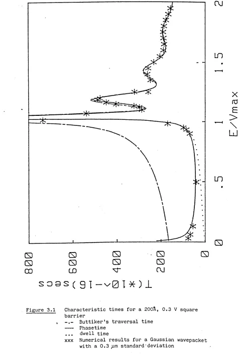
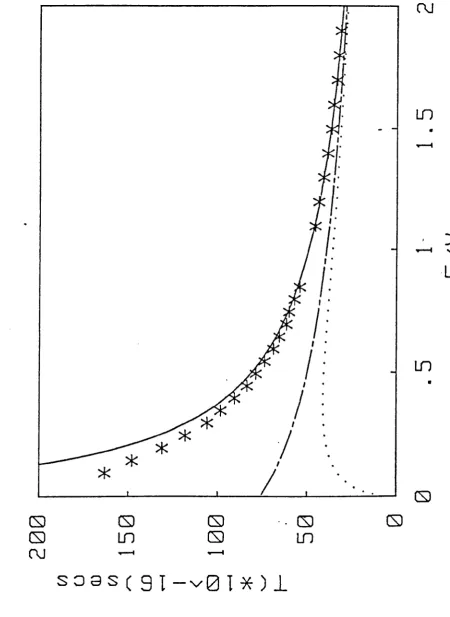
A DISCUSSION OF THE TRAVERSAL TIME OF A BARRIER
Introduction
Derivation of traversal time expression
Single square barriers
Numerical results
Page number
.'
3.6
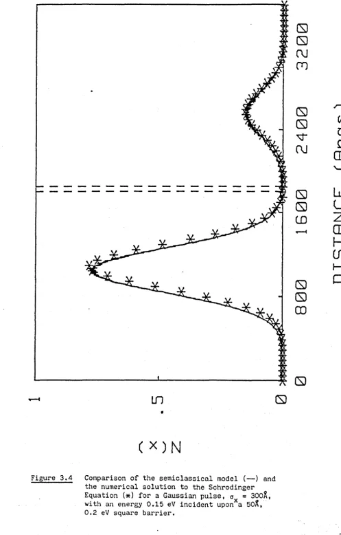
Semi-classical model67
3.7 Summary 70
CHAPTER
4
THE TUNNEL CURRENT AND THE CALCULATION OF THETRANSMISSION COEFFICIENT 72
4.1
Introduction 724.2 Expre~sion for the tunnel current 73
4.3
General analytic technique77
4.4
General numerical technique79
4.5
Simple analytic model83
4.6
Comparison of general techniques90
4.7
Numerical calculation of the phaseshift96
4.8
Simple numerical bandstructure calculation99
4.9
Summary 103CHAPTER
5
CURRENT VOLTAGE CHARACTERISTICS105
5.1 Introduction 105
5.2 Qualitative study of single barrier systems 107
5.3 Qualitative study of double barrier systems 113
5.4
Numerical integration technique and the Fermi level118
5.5
Double barrier systems 1205.6
Affect of external devices
125
5.7 Asymmetry in double barrier systems
129
5.S Other double barrier systems 132
5.9
Systems with more than two layers134
5.10 Triangular and parabolic well potentials 136
5.11 Shewchuk's data 139
5.12
Summary141
SUMMARY AND FURTHER WORK
Summary of thesis
Further work
REFERENCES
(iii)
144
144
152
..
List of Illustrations
Tables 1.1 Figures 1.1
2.1
2.2
2·3
2.4
3·1
3·2
3·3
3.4
4.1
4.2
4.3
4.4
4.5
4.6
4.7
5.1
5·2
Properties of GaAs, AlAs and GaA1As
Parameters double barrier system
Results of four model potentials
Comparison of phase shifts
following ~
13
121
122
24
Basis set for one and two square barriers 29Wave function at moment of impact 37
Comparison of wave function obtained analytically
and numerically 44
Wavepacket transmission probability 46
Characteristic times of a
200A, 0.3
V barrier59
Characteristic times of a25A,
0.1 V barrier59
Magnitude of the wave function in a double barrieras a function of time 63
Comparison of semi-classical model and the exact
result for wavepacket incident upon a barrier
69
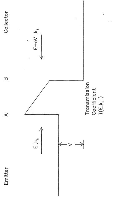
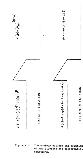
Schematic diagram of situation considered in obtainingthe tunnel current expression 73
Comparison of the solutions of the difference and
differential equations 81
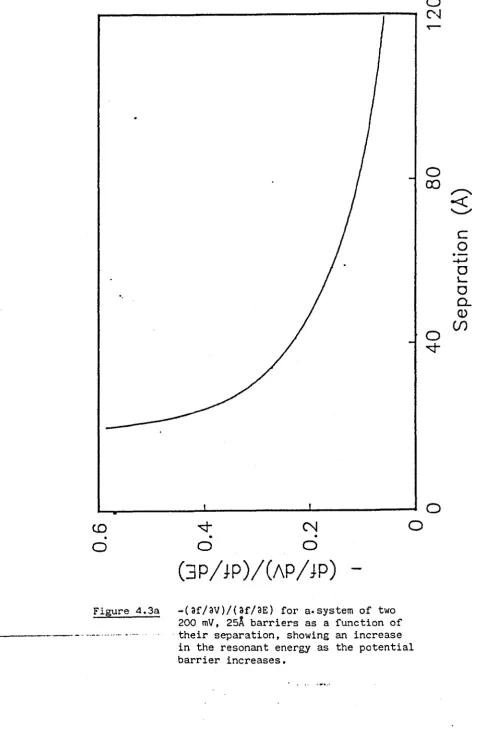
Evaluation of the partial derivatives which control
the rate of change of the resonance energy
87
Error in the numerical results for a single barrier 90Double barrier transmission coefficient 91
Magnitude of resonance in asymmetric double barrier
systems 94
Comparison of the numerical and exact phaseshifts
calculated for a single square barrier
99
Temperature dependence of the current with lightlydoped contacts
117
Temperature dependence of the current with heavily
.-5.3 Temperature dependence of the Fermi level 120
5.4 Observed and 'predicted I-V characteristics of
double barrier system 122
5.5a Affect of series diode on predicted I-V characteristics 126
5.5b Affect of series resistance on predicted I-V
characteristics 126
5.5c Possible discontinuities in I-V characteristics 127
5.6 Affect of different contat doping levels on double
barrier I-V characteristics 130
5.7
Affect of depressing the central layer on the I-Vcharacteristics of a double barrier system
133
5.8a Position of resonances for a system of three barriers 134
5.8b Magnitude of resonances for a system of three barriers 134
5.9
I-V characteristics of a three layer system 135 _5.10 I-V characteristics of triangular barrier at 300 K 136
5.10 I-V characteristics of triangular barrier at
77
K 1365.11 Results of "hot electron spectrometer" 138
5.12 Transmission coefficient of triangular barrier at various voltages
5·13
5.14
5.15
5.16
I-V characteristics of triangular barrier
Schematic diagram of a parabolic well potential
I-V characteristics of the potential in figure (5.14)
Fit to Shewchuk's data at 300 K
6.1 Potential diagram showing accumulation and depletion regions
(v)
138
138
139
139
140
Acknowledgements
There are many people who have helped me to reach the stage at which I am
able to submit this thesis. Some of them I would like to thank
here:-My wife and parents for the sacrifices which allowed me to continue my
education.
Or J
R
Barker for inspiration and guidance.My colleagues at Warwick, and more recently RSRE, for their co-operation
and friendship. Special thanks to Dr D Lowe for his constant willingness
to discuss my problems and for reading this thesis.
Professors P W McMillan and A J Forty for use of the facilities of the
Physics Department and the SERC for financial support.
Finally Mrs C Edge for her cheerful dedication to the typing of this
.-Declaration
This thesis contains an account of my own independent research work
performed in the Department of Physics at the University of Warwick
between October 1982 and October 1985 under the general supervision of
Dr John R Barker.
Some of the work has previously been published as
f~llows:-1. "Theory of Transient Quantum Transport in Heterostructures"
J R Barker, S Collins, D Lowe and S Murray.
Proc 17th lnt Conf Phys Semicon, San Francisco (1984)
Ed J D Chadi and W A Harrison
Springer-Verlag, New York (1985)
2. "On the accuracy of the effective mass approximation for scattering
at heteroJunctions"
S ColI ins, D Lowe and J R Barker
J Phys C 18 L637 (1985)
3.
"Quantum Theory of hot electron tunnelling in microstructures"J R Barker
An invited paper at 4th lnt Conf on Hot Electrons in Semicon
Physica l34B 22 (1985)
INTRODUCTION
Motivation
The advances in.the growth technologies for compound semiconductors in the
past decade have made possible the controlled, reproducible fabrication of
structures with features on a nanometre scale (1). This has motivated
investigations into structures which exploit Quantum Mechanical effects,
with a general aim of manufacturing devices controlled by Quantum
Mechanics.
The structures which are of interest in this thesis were first suggested
by Tsu and Esaki (2). They showed that the transmission resonances,
predicted as early as 1952
(3),
could be exploited to give a resonantcurrent. However, the results at that time were not sufficiently
encouraging to sustain interest, with no resonance being observed at room
temperature.
The advances in fabrication technology since this early work have led to a
renewed interest based on the expectation that the improved sample
fabrication now possible would lead to room temperature resonance. The
first observation of room temperature resonance was reported. by Sollner et
al
(4).
These.resonances, however, could only be detected in the firstderivative of the current. It was nearly two more years before Shewchuk
et al (5) observed a resonance at room temperature.
At present, a stage has been reached at which a resonant current has been
observed at room temperature, but, several unanswered questions remain:
Why is the peak to valley ratio so diasppointingly small? Why don't the
current voltage characteristics show the expected symmetry with respect to
the direction of the bias? Why did the data obtained by Shew~huk et al
contain a discontinuity?
The aim of this. thesis is to provide a theoretical model to address these
questions and to provide a method of predicting the characteristics of
other systems which may be proposed in the future. To be widely useful
restrictions must be place1 on the type of model, it must be easy to
implement, flexible and quick.
A simple current voltage expression is therefore required and it must be
shown that it can at least give a good estimate of the magnitude and shape
of the observed characteristic.
Outline of the Thesis
The expression which is to be used will not b~ derived until Chapter
4.
Before then several points implicitly assumed in the derivation of the
expression will be justified.
In the first chapter a simple one dimensional Schrodinger equation (S.E.)
for the wave function in a Gallium Aluminium Arsenide (GaAlAs) system,
with an Aluminium mole fraction which varies in one dimension will be
given. The equation arises from the work of Bastard
(6)
which will be discussed to show that the assumptions made can be Justified and to obtaincriteria for the applicability of the equation.
The available values for the parameters needed to model both electrons and
shown that there is considerable doubt concerning the accuracy of some of
the values, doubts which mean that the results of methods not requiring
knowledge of the hole masses will be favoured when deciding the best
experimentally determined value of the conduction band discontinuity. The
last section of~e chapter will consider previous criticism of the simple
equation to show that misunderstandings caused overestimates of the errors
involved in using the equation.
The next two chapters are concerned with the results of the one
dimensional time dependent equation which arises from the simple model.
In chapter two, it is shown that the solution to the time independent
equation arises naturally in the solution of the time dependent equation.
This Justifies the later use in the current expression of the results of
the time independent equation, even though the current is carried by
electrons whose behaviour can only be predicted using the time dependent
equation.
In the next chapter, Chapter
3,
the time required by a wavepacket totraverse a potential barrier, the traversal time, will be considered. It
will be shown that, if the wavepacket has a sufficiently well defined
momentum, the traversal time is related to the derivative of the phase
difference between the incident and transmitted waves with respect to the
wavevector. The main point of this chapter will be to demonstrate that
the tunnelling of an electron through a potential barrier is a rapid
process, typically taking of the order of ten femtoseconds. This is
faster than the mean free time which is of the order of a picosecond so
that the probability of an electron being scattered during tunnelling is
assumed to be negligible, allowing scattering to be neglected in the
derivation of the tunnelling current.
At the beginning of Chapter
4
the current expression itself is derived. The expression shows that to be able to calculate the current across ageneral potential a method of calculating the transmission coefficient of
a general potential is required. The remainder of the chapter is devoted
to demonstrating-that a numerical method is much more accurate than the
popular WKB method, and can be extended to calculate traversal time and
the bandstructure of a superlattice.
In the final chapter the current expression itself is used. Initially the
integrand is approximated to demonstrate that the expression can be used
to qualitatively explain the observations of Collins et al (7), and to
predict the behaviour of systems with two layers of GaAlAs separated by
one layer of GaAs. The remainder of the chapter is concerned with the
numerical evaluation of the current expression for systems which have
either been fabricated or proposed for fabrication. The model developed
will be shown to fit the observations to an accuracy which is sufficient
for the model to be useful in predicting the behaviour of proposed
devices. The lack of agreement for one system can be explained as a
failure of one of the assumptions which is included in the model to
simplify the integration over the electron distribution. This failure
does not imply that the model should not be used but indicates that care
is needed in applying the model to ensure that the conditions needed for
the model to be applicable do occur.
The overall conclusion of the thesis is that the current density
expression developed in section 4.2 Is based on a justifiable heuristic
approach. The expression itself is accurate enough to be used in
assessing and understanding devices if the electrons in the contacts are
BJ\CKGROUND, A SIMPLE MODEL FOR A HETEROSTRUCTURE
1.1 Introduction
The aim of this chapter is to outline a simple model obtained by Bastard
which allows a semiconductor with position dependent composition to be
modelled using an equivalent electrostatic potential. This considerable
simplification is vital in obtaining a simple picture of resonant
tunnelling and a method for calculating the current.
The chapter itself is organised into three distinct sections. In the
first section Bastard's work is outlined to show that the assumptions used
to extract a simple model equation from the equation representing the
bandstructure are Justifiable.
The second section is devoted to a discussion of the properties of OaAs,
ALAs and GaAlAs which enter the model as parameters. This discussion will
outline the reasons behind the values for the parameters which will be
used later and to show that the materials are not sufficiently well
characterised to allow experimental verification of the simple model.
With experimental verification excluded, two theoretical tests of the
accuracy of the model are considered. The authors of the original work
are critical of the simple model, however it will be shown that the
criticism arises from misunderstandings concerning the model. The overall
conclusion is that an accuracy of better than ten percent is expected.
The chapter concludes with a short summary section •
1.2 Theoretical model for a heterojunction
In this section Bastard's work will be outlined to Justify the simple
representation of heterostructures used later in the thesis. When
considering elec~ron transport in semiconductor structure, one of the
fundamental properties is the distribution of allowed electron states, the
bandstructure. The most accurate available method of obtaining a
bandstructure is to represent the ions and their associated bound
electrons by a pseudopotential and expand the wave function of the
remaining electrons using an appropriate basis set. Since the unknown
electron distribution gives rise to a contribution to the potential, the
wave function must be iterated until a self-consistent ground state is
obtained.
This procedure is not ideal. The large amount of computer facilities
required and its sophistication restrict its present use to specialist
groups working on small systems. It is also difficult to gain any insight
into the processes governing the formation of the bandstructures making
trends difficult to identify and requiring a study of each individual
system of interest.
The restrictions of the pseudopotential method mean that although it is
the most fundamental available technique its usefulness is limited to
studies of individual systems. These studies indicate the approximations
which can be used to obtain a method simple enough to be used to study
many systems.
A1As-GaAs interface. The most significant result for this thesis is that
the self-consistent pseudopotential for the interface shows only small
differences from the bulk pseudopotentials used as the initial condition.
These small differences are localised within -10~ of the As layer which formed the interface.
The fact that this calculation showed that in GaAs-A1As heterojunctions,
the heterojunction is a region of sharp transition between apparently bulk
materials has led to several models in which a heterojunction is
represented by juxta positioning bulk bandstructures
(6, 9,
la, 11,).In the first of these, Bastard used the two band Kane representation of a
bulk bandstructure (12) to obtain a simple model for heterostructures. In
this representation the conduction and valence band states have the
symmetry of the 5 and p atomic orbitals respectively. This led Bastard to
denote the conduction (valence) band states as S (p) and the conduction
band minimum (valence band maximum) as V (V).
s p
The wave function in a material, A, was expanded as a sum over all the
bands, of
A
centre uj
the Bloch cell periodic part of the wave function at the
A
, multiplied by a slowly varying envelope function Fj ,
zone
If this wave function represents an electron near to the conduction band
minimum only two of the F's are significant, corresponding to the two spin
states representing the conduction band minimum. These two functions,
labelled Fl and F2 by Bastard, are coupled by eigenvalue equations.
Bastard used several assumptions to obtain a simple set of coupled
equations for Fl and F2 and then decouple them to obtain a simple S.E. to
model a heterostructure. These assumptions are:
(i) The momentum matrix element, w , is equal in both materials
(ii) The spatial localisation of any potential perturbation is small
compared to the scale of variation of the envelope
(iii) The only affect of the potential perturbation at the interface is to
sh1ft the bandstructures relative to each other
(iv) The transverse wavelength is greater than the thickness of all the
layers.
Assumption (i) is Justified by the recent work of Merian and Bhattecharjee
(13)
which shows that although n is composition dependent the totalvariation is only a small percentage of the mean value.
The work of Pickett et al
(8)
showed that the potential perturbation islocalised to a few atomic planes. The perturbation is therefore on the
same spatial scale as the cell periodic component u· , which by ~
definition, is a much shorter scale than any variation in F. Assumption
(ii) is therefore justified.
Pickett's work can also be used in an attempt to justify assumption (iii),
to mix states from different bands.
The requirement for the last assumption arises from a need to decouple the
continuity conditions which must be imposed upon the functions. The
coupled continuity conditions are the continuity of
1
EA + E - Vp
and
EA + E - Vp
1 [ -/2
~~.
+ ik_ F, ]where EA is the band gap of material A and
These equations are decoupled if the second term in each bracket can be
neglected. Since the derivative can be approximated by the envelope
function divided by the layer thickness, the second terms are negligible
if the electrons wavelength is much greater than the layer thickness.
That is when assumption (iv) is valid. The approximate nature of the
requirement for assumption (iv) means that it is not a strict condition.
However, it does indicate that care is needed at high temperatures for
thin barriers, for example a
50
~ barrier requires that the transverse energy ET is such thatET < 22.6 meV
which cast doubt on the use of the model at room temperature.
The last assumption decouples the equations produced using the other three
assumptions, so that if all four are valid, the equation for one of the
two envelope functions is (6)
fvs(
z) + nZ- pl
32n2
Pz
31 p+ + n2 p+ 1 _ ... P_ +
EA+E-VprZ) 3 EA+E-Vp (.z)
F
=
EF(1.2.1)
where P±
=
(Px ±iPy )/12. All the variables in equation (1.2.1) arefunctions of z alone, therefore F is separable. The translational
symmetry of the Hamiltonian perpendicular to z means that the envelope
function must take the form
F(x,y,z)
=
fez) exp (l(kxx + Kyy»Defining the constant of motion
Et
=
1'1 2 (kx 2 + ky 2 )2mA
and writing the total energy as the sum of two components
E
=
Et + Ezthe equation for f(z) is
Cl 1 Cl
Clz m(z) Clz + v s (z)
where the mass m(z) is defined as
(1.2.2)
A further simplification is obtained if the energy is assumed to be in the
small range such that for all z
so that m(z) can be replaced by the conduction band minimum mass. This
approximation is only valid for electrons near the conduction band minimum
for all compositions present, which restricts both the energy and
composition range for which the simplified equation with an energy
independent mass is valid.
Despite the limitations imposed by this further Simplification, the
simplicity achieved means that it is the simplified model which will be
used throughout the remainder of the thesis so that in further discussion
m(z)
=
3 (EA + V (z) - V (z»411' S P (1.2.4)
The model has so far excluded any external potential such as would arise
from an electrostatic field. To extend the model to be useful in
GaAs/GaAlAs devices these must be included. Altarelli
(70)
has shown thatif an applied potential is included in the k.p. model the potential is
added to the diagonal elements of the Hamiltonian matrix so that an
applied voltage V(z) can be simply included in Bastards model to give
This shows that the conduction band edge can be simply interpreted as
being equivalent to an electrostatic potential.
A model has therefore been obtained in which the envelope function obeys
equation (1.2.2) with the mass m(z) defined by equation (1.2.4).
The position dependence of both v~z) and m(z) in equation (1.2.2) shows
that a heteroJunction can be represented by a step potential, whilst the
Kronig Penney model can be used to represent
a
superlattice. These aretwo of a class of problems in which the behaviour of the potential changes
discontinuously. In these problems it is usual to solve the wave
functions on each side of the discontinuity and then match the
wavefunctions using continuity conditions. The exact nature of the
continuity conditions is important in section 1.4 and so they will be
discussed here.
The continuity conditions obtained by Bastard, after decoupling, require
the continuity of
f I 1 gf
m(z) az
where m(z) is defined by (l.2.3) but can be approximated by (1.2.4).
These conditions arise from the Hamiltonian directly and must therefore be
the correct continuity conditions. A conclusion supported by Morrow and
Brownstein
(69).
1.3 Properties of GaAs, AlAs and GaA1As
In this section the known properties of GaAs, AlAs and GaAlAs required for
will show that attempts at experimental verification of (1.2.2) are
premature, and provide the best estimates of the required parameters for
use later.
All three materials.form a Zinc Blende structure, with one sUblattice in
GaAlAs containing both Ga and Al ions. This crystal structure leads to a
first Brillouin zone with several points of high symmetry amongst which
r(O,O,O),X(l,O,O) and L(Yz,Yz,Yz), representing local conduction band
minima, are important.
To begin, consider the best characterised of the three materials GaAs, a
direct bandgap material with both the conduction band minimum and valence
band maximum occurring at the
r
point.Although GaAs is well characterised, there are still uncertainties about
several of the accepted values, especially the hole masses. These
uncertainties arise because the valence band maximum is formed by two
degenerate anisotropic bands, denoted as the heavy hole and light hole
bands. The degeneracy means that experiments yield signals from two
bands, whilst the anisotropy can lead to a wide variation in the
experimental values obtained for the same parameter. The evidence agrees
that the [1,1,1] direction 15 the heaviest In both bands, however the
degree of anisotropy differs from experimental values of 25% or 50%
(14) to a theoretical value of approximately 100% (15). These
difficulties mean that the values listed in Table 1.1 for the hole masses
are concensus isotropic values for anisotropic parameters. A list of
parameters for AlAs is more difficult.to compile. AlAs is an indirect
material with the conduction band minimum at the X point lying below that
at the rpoint. This makes the bandgap of interest, the direct bandgap,
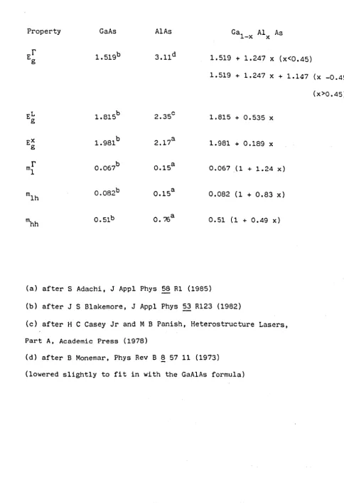
TABLE 1.1
Property GaAs ALAs Gal Ai As
-x x
Er
g 1. 519b 3.11 d 1. 519 + 1.247 x (x<0.45)
1.519 + 1.247 x + 1.147 (x -0.45) 2
(X>0.45)
EL
g 1. 815b 2.35c 1.815 + 0.535 x
EX
g 1.981
b 2.17a
1.981 + 0.189 x
mr
1 0.067
b 0.15a
0.067 (1 + 1.24 x)
m
1h 0.082b 0.15
a
0.082 (1 + 0.83 x)
"'hh
0.51b O.76a 0.51 (1 + 0.49 x)(a) after S Adachi, J Appl Phys ~ Rl (1985)
(b) after J S Blakemore, J App1 Phys 53 R123 (1982)
(c) after H C Casey Jr and M B Panish, Heterostructure Lasers,
Part A, Academic Press (1978)
(d) after B Monemar, Phys Rev B ~ 57 11 (1973)
(lowered slightly to fit in with the GaA1As formula)
[image:24.584.69.554.71.778.2]-difficult to measure.
Several attempts have been made to measure the direct bandgap of AlAs.
The only low temperature measurement seems to be due to Monemar et al (16)
and gave a value· of 3.13 eVat 4K. All the other measurements were at
room temperature and gave values of 3.03 eV (16), 2.95 eV (17) and
3.14 eV (18). The high value given by Yim (18) can be attributed to the
technique used. From an absorption spectra, the bandgap was calculated by
extrapolating the linear part of the absorption against photon energy
curve to zero absorption. This was done without first subtracting off the
indirect contribution, a failure which can lead to an overestimate.
The conclusion is therefore that the bandgap at absolute zero is
approximately 3.13 eV, with a decrease to approximately
3
eV at roomtemperature. The value given in Table 1.1 is slightly less than 3.13 and
is chosen to fit in with the expression given for the bandgap of GaA1As.
The electron mass required for the model is the
r
valley mass, a parameterwhose measurement is made more difficult by the indirect nature of the
material. The only measurement, by Monemar et al (16), gave an estimated
value, from an examination of the exitonic spectrum of AlAs of
.
-31m
=
0.113 x 9.109 x 10· kgThe lack of further experimental data means that consideration should be
given to theoretical values.
A self-consistent orthogonalised plane wave calculation performed by
Stukel and Euwema (19), with only the lattice parameter as input, gave
m
=
0.105 x 9.i09 x 10-SI kgwhich is in general agreement with the value obtained from a k.p.
calculation by Braunstein and Kane (20)
m
=
0.110 x 9.109 x 10-'1 kgThe value given by Braunstein and Kane for the conduction band mass in
GaAs was 15% higher than the currently accepted value. This can be used
to give an estimated error for the AlAs value of
m
=
(0.110 ± 0.017)x
9.109x
10-11 kg(1.3.1)
with the expectation that the-true value is at the lower end of the range.
Although the value tabulated is the widely accepted value it would appear
that this Is an overestimate and a better value would be (1.3.1), which
would make the light hole mass greater than the conduction band mass, as
in GaAs.
It appears that the hole masses in AlAs have never been measured. The
tabulated values are the accepted values which appear to originate in the
work of Lawaetz (80). In this early paper the then accepted values for Si
and Ge parameters were used to estimate the properties of compound
semiconductors. It should be stressed that the values are estimates,
which Lawaetz hints contain large errors, since, to obtain any value at
all, the y parameters used had to be quoted to a greater accuracy than the
heavy hole mass is in error by approximately twenty percent and the light
hole mass is in error by approximately ten percent. This leads to
estimates for AlAs of
m
l
=
0.15 ± 0.01; (x 9.109 10·' lkg) mh
=
0.76 ±0.15 (x 9.109 10·l1 kg )The more recent CPA calculations of Chen and Shur (15) gave the values for
ml[l,l,l]
=
0.137ml[l,O,O]
=
0.103mh[l,l,l]
=
1.053mh[l,O,O]
=
0.435(x 9.109 10·'lkg)
(x 9.109 10·'lkg)
(x 9.109 10·'lkg)
(x 9.109 10·'lkg)
Whilst these can only be used as estimates for the AlAs masses they do
show the high degree of anisotropy in the hole masses and could be used to
support an argument that the tabulated light hole mass is an upper bound,
being equal to the highest anisotropic value.
It must be concluded that the masses given for AlAs in Table 1.1 are only
the currently accepted estimates and further characterisation work is
needed.
Despite the uncertainty in the values for some of the properties of the
binary compounds estimates are required for the properties of tertiary
alloys. A simplistic approach to obtain the GaA1As parameters is to
interpolate between the values for GaAs and AlAs. Then, for an alloy with
an Al molefraction X, a parameter p is estimated as
p(x)
=
(l-x)p(o) + x p(l}A lack of experimental results means that this approach is used at present
to obtain all the effective masses in GaAIAs, although another approach is
I
suggested by k.p. theory (20), which gives the conduction band and light
hole band masses as
..l.
1 + 2plUg
Eg!Ao )
=
+m 3n1
C
1
1 - 4Pl
=
mR,.
3fi1E g
For GaAs and AlAs, the spin split off energy 6. is much less than the
bandgap Egl so that the conduction band mass can be written as
=
Then, since both expressions are dominated by the second term and the
matrix element P has been shown to be approximately constant to a first
approximation the masses will have the same compositional dependence as
Eg.
There are several studies of the variation of bandgap with composition.
Obtaining a conclusive answer is difficult, a point clearly demonstrated
when different techniques obtained different results from the same samples
The tabulated formula is the one which appears to be the most widely
accepted and seems to originate in unpublished work (22). The formula
has a discontinuous change at an Al molefraction very close to that
associated with the change from a direct to an indirect bandgap. This has
lead Chen and Sher, whose CPA calculation showed no such behaviour, to
claim that the discontinuity is caused by experimental error in
determining the direct bandgap in an indirect material.
A different viewpoint can be taken (23) by considering the more usual
expression for the dependence of the bandgap on composition
If the non-linearity, measured by the bowing parameter c, is mainly caused
by alloy scattering, then c itself may be composition dependent. A
conclusion supported by the ePA calculations which show a bowing parameter
which is dependent on x. The tabulated formula would then be considered
as a simple fit, with composition independent bowing parameter, to
experimental data which shows composition dependent bowing and would
therefore be expected to change as further measurements improve the known
data.
The most important property of a GaA1As system is the manner in which the
bandstructures of two layers with different compositions align at a
heteroJunction. The usual method of expressing this alignment is to quote
the difference in the energies of the
r
point conduction band minimaacross the heteroJunction as a fraction of the total difference in the
direct bandgaps, Q. There is an implicit assumption that this is constant
for all systems, which means that doped heteroJunctions, in which charge
transfers to the low bandgap material, are excluded and that the results
of Waldrop et al (24) will eventually be shown to be due to an
uncontrolled variable, which caused apparently identical heterojuntions to
give rise to different discontinuities.
Until recently it·was widely accepted that the value for Q was
0.85,
aresult obtained by Dingle (25). More recently, results have tended to
show this to be an overestimate.
The "Dingle Rule" was obtained from the absorption spectra of quantum
wells by matching a simple model for the expected electron and hole energy
levels to the observed transitions. This or the related luminescence
experiment have proved very popular, with the more recent work by Miller
et al (26) on parabolic and square quantum wells giving
Q
=
0.57and the results from square wells, by Dawson et al (27)
Q
=
0.75Although this technique is widely used the three papers(25,26,27~
demonstrate some of the difficulties which arise. All the authors assume
that the simple model derived in the previous section is correct. The
different authors use different connection formulae to obtain the
eigenstates, a difference which leads to significantly different energy
levels for the same parameters. The uncertainty in the hole masses means
that Miller et al are justified in using the hole mass as well as Q as an
adjustable parameter, and the uncertainty in growth allows Dawson et al to
The conclusion is that, by assuming the validity of the simple model and
the values of some of the parameters, this technique is assuming too much.
Consequently it is not a good technique for obtaining
Q
unless sufficient data is obtained to allow Q and all the masses to be variables and stillhave sufficient data to prove the validity of the model. A technique is
•
therefore required which assumes neither the validity of the simple model
or the values of the effective masses.
Such a technique is C-V profiling which can be used to obtain Q. Since
its original use by Kroemer (28) the technique has been improved by
Watanabe et al (29). After extracting the value for Q, it has been shown
that the result can be checked by modelling the measured carrier
concentration, demonstrating the measurements sensitivity to
Q.
The other advantage of the C-V technique is that by using n and p type doped GaAs itis possible to obtain the conduction band and valence band discontinuities
separately. The fact that Watanabe et al obtained results which exactly
added up to the bandgap difference was used as an indication of the
accuracy of the technique.
The result obtained using this technique was
Q
=
0.62a result which was supported recently by Heiblum et al (30) from an
examination of the photocurrent across a sample containing a
heteroJunction.
In the past, agreement with this result has also been claimed from a hole
mobility experiment
(31).
A model of the hole mobility in the twodimensional electron gas next to the heteroJunction was used to extract a
difference in hole band maxima of 220 meV, the total bandgap difference
being obtained from a photoluminescence measurement. The samples Al
molefraction, 0.5, meant that the material was indirect and the measured
value, 550 meV, is much closer to an estimate of the indirect gap,
562 meV, than the estimated direct gap, 626 meV. The conclusion is that
Wang et al measured the indirect gap and the true value of Q, using the
estimated direct gap is
Q
=
0.67 ± 0.05which is in good agreement with the analysis they produced of the results
of a similar experiment by Stormer
Q
=
0.69 ± 0.04Despite this it would appear that the best estimate of Q presently
available is
Q
=
0.62, a conclusion which is supported by the recent theoretical model purposed by Tersoff(32),
a model experimentallyverified
byMargaritondo
(33).
One final point which should be made is that although the bandgaps
themselves are temperature dependent, there is some evidence (34) that the
temperature dependence of the bandgap is independent of the composition.
This means that the bandgap difference across a heterojunction is
temperature independent, with the consequence that the potentials used to
1.4
Comparison between the simple model and other modelsA direct comparison between the results of a tight binding calculation and
those of the simple model from section 1.2 for the transmission
coefficient for
a
single layer has been performed by Osbourn(35).
Thelayers studied were chosen to be sufficiently thick that the transmission
coefficient from the simple model could, to a good approximation, be
written as
T
=
A exp (-2ICd)where d is the layer thickness.
Using this form Osbourn obtained the value of ~ which would be required to
fit the tight binding calculation. The required value was found to be
smaller than the value which Osbourn claimed arose from the simple model,
the difference increasing with Al molefraction. The conclusion was
therefore reached that the simple model was inaccurate.
In the above analysis the decay constant was defined as
I(
=
[
2m(V-E)] Yz
1'\2
as would be expected, however, the potential V was taken to be the total
bandgap difference rather than the conduction band difference. Osbourn
therefore overestimates the value of I( which would arise in the simple
model, a fact which could explain the discrepancy observed. The
compositional dependence of the disagreement then arises because the
overestimate increaseas with composition. This misunderstanding
invalidates Osbourn's conclusion.
A more recent comparison was performed by Marsh and Inkson
(9,36).
Thecomparison, based on empirical'pseudopotential calculations,of the
phase shift suffered by a wavefunction reflected from a heterojunction,
concluded that the simple model was very inaccurate and could ?ot be
expected to give·any quantitative predictions of the properties of systems
containing heterojunctions. As with Osbourn this conclusion can be shown
to be based on a misunderstanding concerning the simple model
(37).
The expression used by Marsh and Inkson for the phase shift calculated
using the simple model was
This expression arises when the wavefunction is matched across the
heterojunction using the continuity conditions which require the
continuity of
f , Clf
az
(1.4.1)
For comparison the result obtained using the continuity relations which
arise naturally in the model, which require the continuity of
is
f , 1 H
m az
~
=
arc tan 'Ifwhere m1 and mz are the masses in GaAs and GaA1As respectively.
(1.4.2)
To compare the results of the pseudopotential calculation and the correct
formula (1.4.2), a value for the potential V is required which is
function of VIE and so a fit to the curve obtained from (1.4.1) will give a unique value for V.
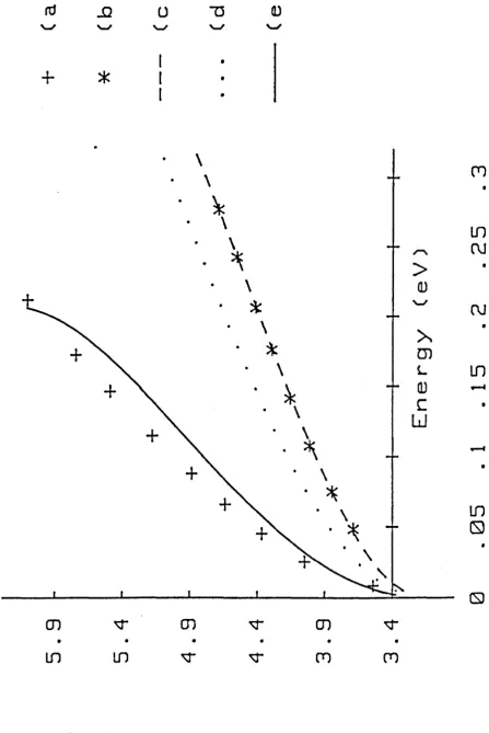
In figure (1.1) the results obtained for an A1 mo1efraction of 0.25 are
shown. The given curve from expression (1.4.1) is shown as curve B which
was fitted (curve C) to obtain the potential V. This value was then
inserted into the correct formula (1.4.2) to give an improved, but
unsatisfactory result (curve D). This remaining disagreement can be
reduced further if the value of V extracted from curve B is considered.
The fitting procedure shows that a potential corresponding to more than
1.5 times the accepted bandgap difference between the two materials was
used in (1.4.1), an error which may in part be due to following Osbourn's
definition of the decay constant.
To use the simple model properly a value for the conduction band
discontinuity is required which is as consistent as possible with the
results of the pseudopotentia1 calculations. To do this the conduction
band discontinuity was taken to be the accepted bandgap difference minus
the valence band discontinuity 6Ev given by Marsh and Inkson
v
=
1.247x 6Ev eVThis is not the exact value which should be used, since the
pseudopotential method doesn't give the exact bandstructure, but, if the
pseudopotentials do give a good model of a real heterojunction, this must
be a good approximation. The result of using this value of potential in
the correct expression is shown as curve E. The agreement is encouraging,
especially when it is recognised that this is not an optimum fit, but the
u
•
+
*
•
•\
\
*
\
\
~
\
:\:
\
*
\
+
*
\
+
\
~
\
~
fJ
\
•
~
4-
.--t:
tn
ID
01
~01
~01
t1
• • • • •ro
lf1
lf1
~ ~ (T)-t:
CL
Figure 1.1 Comparison of phase shifts calculated from pseudopotentials and the simple model
(a) Pseudopotential result
(b) Marsh and Inkson's result from (1.4.1) (c) Fit to (b) to extract the potential
,-....
>
ID
'-JA
m
LID
C
W
~•
(T)(d) Results of (1.4.2) using the potential from (c)
[image:36.581.103.550.17.686.2]result of using the most accurate parameters available.
More recently Marsh and Inkson
(38)
extended the calculations to evaluatethe eigenenergies of a single quantum well. The eigenvalue equation used
for a well of length L was
kL + a(k) = mw
In this expression a(k) was taken to be the phaseshift between the
incident and reflected components, which in this case was taken to have
two components, one from the envelope function and one from the cell
periodic part of the wavefunction. The simple model cannot reproduce a(k)
because it contains no means of calculating the contribution from the cell
periodic component. This would appear to be a severe criticism until
expression
(1.4.3)
is considered in detail.Condition
(1.4.3)
is exactly the same as that which would be obtainedusing
a
square well model for the Quantum well. The square well is the potential in the S.E. for the envelope function alone and not the totalwavefunction. Therefore, the condition which gives rise to
(1.4.3)
shouldonly be applied to the envelope function and not the total wave function,
giving rise to the eigenvalue equation
~<L + 0(k)
=
mwas originally defined by Marsh and Inkson
(9),
where it was also statedthat the cell periodic contribution to a was expected to be small.
In two of the crystallographic directions studied by Marsh and Inkson the
difference between a and ~ does appear to be small. However, in the
(1,0,0), direction chosen to calculate the eigenenergies of a Quantum
well, the difference is large. In this direction ~ is almost constant
over the entire energy range except for a resonance, but a is a smooth
function very similar to the other results. The smoothing of the resonant
feature by the cell periodic component suggests that the strange behaviour
observed in the (1,0,0) direction is due to the manner in which the phase
of the total wave function is subdivided between the cell periodic
function and the envelope function. If this is correct, then as with the
other crystallographic directions, the difference between ~ and a can be
assumed to be small.
Despite these misunderstandings, the work of Marsh and Inkson remains the
best from which to obtain an estimate of the errors involved in using.the
simple model. The conclusion is therefore that in the worst possible
case, a GaAs/ALAs heterostructures, an error of up to ten percent can be
expected, with smaller errors in GaAs/GaAlAs heterostructures due to the
lower conduction band discontinuity.
1.5
SummaryIn this chapter it has been demonstrated that Bastard used justifiable
approximations to produce a simple one dimensional model S.E. for the
conduction band states in systems with varying material composition.
The model obtained by Bastard requires several input parameters before it
can be used to predict the behaviour of GaAlAs systems, and the accepted
values for the parameters were tabulated. Although there is an accepted
value for all the parameters doubts about the accuracy of several of these
were expressed, doubts which indicate a need for further characterisation
of AlAs and bring into question the use of superlattice
absorption/emission experiments to determine the conduction band
discontinuity. These doubts cast upon the results of superlattice
experiments meant that the results of such experiments were ignored and an
accepted value for Q of
Q
=
0.62was taken from a C-V profiling experiment.
The results of the final section showed that critiCisms of the simple
model by Osbourn and Marsh and Inkson were based on misunderstandings of
the simple model. The work of Marsh and Inkson was corrected to show that
their estimate of errors of 10% for an AIAs/GaAs heteroJunction was good
enough to be taken as a guide to the order of magnitude of the errors.
A point has now been reached at which a simple S.E. can be used with some
confidence to model a GaAIAs/GaAs heterostructure.
THE SOLUTION OF A SIMPLE TIME DEPENDENT PROBLEM
2.1 Introduction
The last chapter·demonstrated that a simple one dimensional model could be
used for systems in which the Aluminium concentration in GaAIAs varied.
The tunnelling current through such a system arises from the motion of
electrons, motion which must be treated as a time dependent problem. In
this chapter it will be demonstrated that a simple formula, which involves
only the solution to the time independent S.E., can be used to calculate
tunnelling currents. This is important later in deriving a current
voltage expression which only requires the solution of the time
independent equation.
In the first three sections the basis sets for two simple model potentials
and the expressions for the transmitted and reflected wave functions will
be obtained. The expressions for the wave functions can be used to give a
simple picture of the processes involved in tunnelling, and show how the
solution to the time independent S.E. arises naturally in a time dependent
problem. The solution for the.double barrier potential shows that the
transmission coefficient has a resonance, a property which can, hopefully,
be exploited and is the major reason for interest in these systems.
In the fourth section a general numerical technique is outlined which can
be used to complement the analytic solution. The major use of this
technique here is to confirm the accuracy of the preceeding analysis.
This is confirmed in the fifth section before a short summary of the
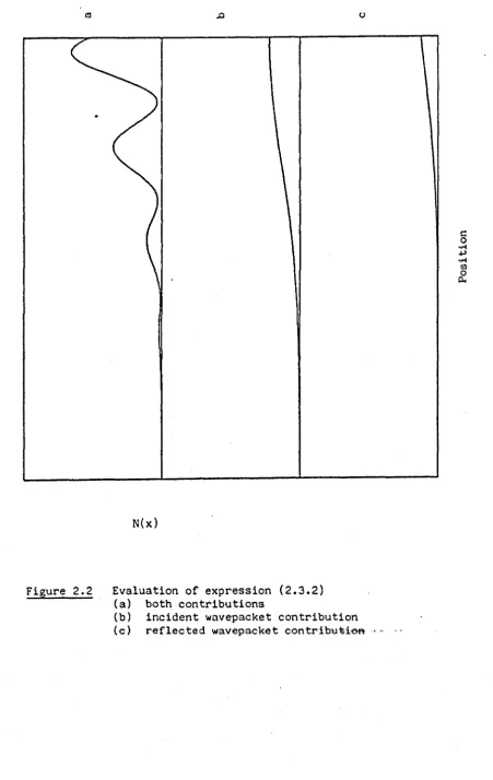
~
03 Q) rn ... rn rn (1) eT rn Hj o '1 o ;:l (1) Q) ;:l 0. eT ~ o (Jl .n c: Q) '1 (1) 0'" Q) '1 '1 ... (1) '1 (J)E
>
VA+ sin(kx+(~+)
A
-
sin(kx+o-)- _ ..
_._---E
<
VA+ cos(kx+O+)
A
-
sin(kx+o-)J
E
>
V+ +
A cos(kx+o) B cos(k'x+y , + +
A
-
sin(kx+o-) B- sin(k'x+y-)E < V
A+ cos(kx+O+) B COSh(KX+Y} + +
-
sln(kx+o-) B- slnh(KX+y-'A
0+ cosk'x A+ cos(kx-O+)
0
-
sink'x A sin(kx-o-)+
B COShKX A+ cos(kx-o+)
-B sinhKX' A
-
sin(kx-o-)C+ coskx
o
+ cos(k'x-y' + A+ cos(kx-O-)C
-
sinkx B- sin(k'x-y-) A- sin(kx-O+)C+ coskx B COSh(KX-Y) + + A+ cos(kx-o-)
2.2 Basis set for a square barrier potential
Before attempting to solve the problem of a wavepacket incident upon a
square barrier, a complete orthonormal basis set is required. The basis
set are the eigen~tates for the Hamiltonian, shown in figure (2.l), which,
because of the symmetry of the potential, can be split into odd and even
parity states, each set having one state at each energy.
The orthogonality of the basis set can be demonstrated in two simple
stages.
(l) Consider any two non-degenerate states ~\ and Vz •
shown
(39)
that these two states must be orthogonal.and
<1jI,IHI~:l> - <~1IHh2>" 0
(E,-E
z) <Vl\VZ
> ..0
The states being non-degenerate means ~ ~ Ez so that
<
V
1/VZ
> ..0
and the states are orthogonal.
It is easily
(2) With all the non degenerate states orthogonallsed it remains to
orthogonalise the degenerate pairs. The orthogonality of degenerate pairs
can be simply demonstrated using the parity of the states, this property
being the motivation for the choice of the co-ordinates.
With the orthogonality of the states demonstrated they must be normalised.
demonstrated for an even parity state with an energy less than that
equivalent to the barrier height. The normalisation integral is
<',Ip
=
2[f::'
S' cosh' . . + f A ' cos'(kx-'+) ]where the parity of the state has been used to simplify the expression.
The next step is to write the integrals in the form
The first integral can be easily performed to give a contribution
+ A.2 [ 4k si.n 2(K3-0+) - sin 20+)
The second integral is more difficult, direct evaluation giving infinity.
Therefore consider
lim
k-+ k'
CD
This can be evaluated split into two contributions.
CD
lim A(k) A(k') (dx {cos «k-k')x - (o+(k)-o+(k'») +
k~k'
2"
~\
Each one of these can then be evaluated by the same technique. Consider
Then the first integral becomes
~ •
~
dy cos«k-k')y) +~dY
cos«k-k')y)Ao
Ak
The first integral must be integrated using
to give
-W o(k) + i (1- 0kJO)
k
JC
dx cos «k-k')x - (e+(k) -o+(k'»)w e(k-k') + 1 (k-k')
=
The problem that arises in normalising the basis set can now be seen. The
free space contribution has given rise to the 6(k-k') term, whilst the
remainder of the wave function has given rise to a finite term. These two
terms require different schemes of normalisation. The 6 function term
requires A to be such that
whilst the other term requires A such that
<liI(k) 1 liI(k) >
=
1These two conditions are mutally exclusive •
•
The only way to proceed is to consider the wave function. The free space
component to the wave function occupies all but the central region of
space. That is all of space except for a small region much less than a
micron in length. It is therefore reasonable to expect the free space
component of the wave function to dominate, therefore, it would seem
reasonable to normalise the basis set in the same manner as a plane wave.
For this reason all the contributions to the integral,
<,I,>,
except forthe ~(k-k') contribution are neglected and the wave function
6
functionnormalised.
This means that the approximation
will
be used so thatA(k)
is a constant with a value of 1/~. With thestates normalised the parameters ~ must be defined to characterise the
states, this is done using the continuity relations
~+ = ka + arc tan (ICtanhlCa/k) . E < V
~+ = ka - arc tan ( 1< ' tank' a/k ) E > V
6
-
:: ka - arc tan (ktanhlCa/lC) E < V-~ = ka - arc tan (ktank'a/k') E > V
where k' :: (2m(E-V) )
~
hZ IC = (
2m~~-E)
)"
2.3 Expansion of the initial condition
Having obtained a basis set in the previous section. The next step is to
expand the initial condition in terms of the basis set so that the
wavepacket can b~ evolved by multiplying each basis function by the phase
factor exp (-iwt) and re-integrating.
There are two possible restrictions which could be imposed to study
tunnelling. The wavepacket can be such that there is either no
probability of finding an electron on one side of the barrier or no
probability of finding an electron with an energy greater than the barrier
height. Two conditions which are made mutually exclusive by the
uncertainty relation connecting wavevector and space. The aim of the
thesis is to study current voltage characteristics due to electrons
traversing a barrier system. This means that the first of these
conditions is more applicable, and is therefore adopted.
The initial condition is such that the wavepacket is restricted at t=O to
one side of the barrier, Region I, so that to reach the other side, Region
Ill, the barrier must be traversed. This is unlike the other condition
where there is always some probability of finding an electron in Region
III at t=O. The expansion coefficients of the initial condition for the
odd and even states are
c(k)
=
~dX' ~(x'o)
A+(k) cos (kx + 6+)s(k)
=
~dX'
v(x'o) A-(k) sin (kx + 6-)These can be written as linear combinations of the fourier coefficients of
the initial condition
f(k) =
j
dx' e ikx' ~(x'o)elk) •. l\+(k) [ eU + f(k) + .-u+ f(-k) ] /2
s(k)
=
A-(k) [eU - f(k) - e -16- f(-k) ] /2The wave function in Region I I I is then the sum of two integrals
CD
[
+ + -iwkt
~(x,t)
=
dkA (k) c(k) cos (kx-6 ) eCD 0
[ - - -iwk
t
+ dk A (k) s(k) sin (kx-6 ) e
o
Using the result, from the previous section, that both the normalisation
+ - .
constants A and A are to a very good approximate given by
l/rn
the twoterms can be combined. The expression is further simplifie~ by noting
that the 6's are both odd functions of k to give
~(x,t)
=
1 2,;f-
.:k f(k) cos (6 -6 ) exp i(kx + 6 +6 - wkt) + - [ + - ]A similar procedure for the wave function in Region I gives
~(x.t~
=
~.
[
~:k
f(k) exp(-ikx-i~t)
+ i
~dk
f(k) sin (a--a+) exp (i(kx-wt+a++!-» ] (2.2.2)If it is remembered that the wave function in free space would be
CD
~(x,t)
=
~w
jdk f(k) exp [-i(kx-wt)]_CD
these result have a simple interpretation. The wave function in Region
III can then be identified as a free propagating wavepacket, with each
fourier component modified by a prefactor which can be identified as the
transmission coefficient for that fourier component. The wave function in
Region I has two components. The first is a free evolving wavepacket,
whilst the other is a wavepacket moving in the opposite direction with
each fourier component premultiplied by a reflection coefficient r(k).
This interpretation means that;
(i) the condition t2 + rZ
=
1 is automatically satisfied.(ii) the phase shifts of the reflected and transmitted fourler components
differ by w/2
(iii) because both the phase angles ~ tend to zero as the barrier width
tends to zero, the solution to the freely evolving wavepacket is easily
recovered.
The most important result arises when the expressions cos2(~+-~-)and (~++6-) are expanded
=
4K'-k 2 + (KZ_kZ)2sinh 2Ka 4K2k2and found to be identical to the transmission probability and phaseshift
which would be obtained by solving the time independent S.E. with a unit
incident flux in Region I. Although this result has been obtained for a