Performance evaluation of the time delay digital tanlock
loop architectures
AL-KHARJI AL-ALI, Omar, ANANI, Nader, AL-ARAJI, Saleh, AL-QUTAYRI, Mahmoud and PONNAPALLI, Prasad
Available from Sheffield Hallam University Research Archive (SHURA) at:
http://shura.shu.ac.uk/10148/
This document is the author deposited version. You are advised to consult the publisher's version if you wish to cite from it.
Published version
AL-KHARJI AL-ALI, Omar, ANANI, Nader, AL-ARAJI, Saleh, AL-QUTAYRI, Mahmoud and PONNAPALLI, Prasad (2015). Performance evaluation of the time delay digital tanlock loop architectures. International Journal of Electronics, 103 (1), 88-112.
Copyright and re-use policy
See http://shura.shu.ac.uk/information.html
Page 1 of 29
Performance evaluation of the time delay digital tanlock loop
architectures
Omar Al-Kharji Al-Ali
1, Nader Anani
2, Mahmoud Al-Qutayri
3,
Saleh Al-Araji
3, and Prasad Ponnapalli
41The Telecommunications Regulatory Authority, UAE
2Dept. of Engineering and Mathematics, Sheffield Hallam University, Sheffield, UK. 3College of Engineering, Khalifa University, UAE.
Page 2 of 29
Performance evaluation of the time delay digital tanlock loop
architectures
This paper presents the architectures, theoretical analyses and testing results of modified time delay digital tanlock loops (TDTLs) systems. The modifications to the original TDTL architecture were introduced to overcome some of the limitations of the original TDTL and to enhance the overall performance of the particular systems. The limitations addressed in this paper include the nonlinearity of the phase detector, the restricted width of the locking range, and the overall system acquisition speed. Each of the modified architectures was tested through subjecting the system to sudden positive and negative frequency steps and comparing its response with that of the original TDTL. In addition, the performance of all the architectures was evaluated under noise-free as well as noisy environments. The extensive simulation results using MATLAB/SIMULINK demonstrate that the new architectures overcome the limitations they addressed and the overall results confirmed significant improvements in performance compared to the conventional TDTL system.
Keywords: Acquisition speed, DPLL, jitter, lock range, noise, TDTL.
1. Introduction
Synchronization between two electrical signals is fundamental to the proper
operation of many electronic systems such as communications, signal processing and
control systems (Chyun and Hung, 1996; Lindsey and Chak,1981; Gardner, 2005).
Achieving this kind of synchronization has been achieved using phase-locked loops
(PLL) (Terng-Yin, Bai-Jue, and Chen-Yi,1999; Best,2007;Crawford,2007). More
recently, in the area of renewable energy and localized power generation (Pearce, Al
Zahawi, and Shuttleworth, 2001;Pearce,Al Zahawi, Auckland,and Starr, 1996 ), PLLs
are primarily used for the synchronization of local generators with the low voltage
utility grid (Anani, Al-Kharji Al-Ali, Ponnapalli, Al-Araji, and Al-Qutayri,2012a,
2012b).
Fundamentally, a PLL is an electronic system which operates by detecting the
difference in phase between an incoming signal and the output signal of a local voltage
controlled oscillator (VCO) (Gardner, 2005). The result of this detection is
subsequently employed to minimize or eliminate the phase difference between the said
Page 3 of 29 Advances in digital and integrated circuit technologies, led to the development
of digital PLLs (DPLLs), which are typically classified as either uniform or a
non-uniform based on the sampling technique they use to sample analogue signals.
Non-uniform DPPLs are more attractive due to the ease of their modelling and circuit
implementation (Lindsey, 1981). The zero-crossing Digital phase-locked loop
(ZCDPLL) and the DTL (Jae, and Chong, 1982; Hussain, Boashash, Hassan-Ali, and
Al-Araji, 2001; Al-Araji, Al-Qutayri, and Al-Moosa, 2004; Al-Kharji Al-Ali et al.,
2012a) are examples of the non-uniform DPLLs. The advantages of the DTL include
good linearity and reduced sensitivity to variations in the power of the input signal.
However, the DTL uses a Hilbert Transformer (HT), which is clearly a disadvantage
due to its implementation complexity (Guan-Chyun, and Hung, 1996). Later, this
implementation issue was alleviated by the introduction of the time delay digital tanlock
loop (TDTL) (Hussain et al., 2001; Al-Kharji Al-Ali et al., 2012b) in which the HT was
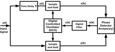
replaced by a fixed time delay unit, Figure 1.
y(t)
Time Delay τ and HoldSample
Sample and Hold
Digital Controlled
Oscillator (DCO)
Digital Filter
Phase Detector Arctan(x/y)
x(t) x(k)
y(k) Input
Signal
[image:4.595.190.423.463.569.2]e(k) c(k)
Figure 1. Block diagram of the first-order TDTL architecture.
However, the conventional TDTL has few shortcomings that limit its
performance. These include the nonlinearity of the phase detector and the finite
non-zero phase error in the locked state of the first-order TDTL system. Additionally, the
second-order loop has a limited locking range and acquisition speed that can be
Page 4 of 29 limitations. Comparison between the performances of the original TDTL and the
proposed architectures are also presented. Tests were performed using a variety of input
signals under noisy and noise-free conditions.
Section 2, of this article, gives the mathematical analysis of the original TDTL
and its MATLAB/Simulink simulation results are given in Section 3. The
fundamental limitations of the basic TDTL are analysed in details in Section 4. New
improved TDTL architectures are also presented in this section. The performance of
these new architectures in noisy environment is presented in Section 5. Finally, the
paper is concluded in Section 6.
2. TDTL Mathematical Analysis
In this section, the TDTL is mathematically modelled and analyzed under noise-free
environment. The analysis is based on the model presented in (Jae, and Chong,1982;
Al-Kharji Al-Ali et al., 2012). The TDTL loop takes an input sinusoidal signaly t with
a frequency offset Δ( o), which is converted to a phase shift. This phase shift is
measured with respect to the free-running frequency oof the DCO (digital controlled
oscillator) as described below
o
y t Asint t (1)
where A is the amplitude of the signal and
t Δ t ois its phase process, whilst ois a constant. The input signal is passed through a time delay unit , as indicated in
Figure 1, which produces a variable phase shift ‘lag’ whose value depends on
the frequency of the input signal. As a result, a phase shifted signal x t
of the incomingsignal is produced as
x t Asinot t (2)
Page 5 of 29 and hold blocks as depicted Figure 1. As a result, sampled versions of the signals are
generated as
o( )
y k Asint k k (3)
and
o( )
x k Asint k k (4)
where
k t k
The sampling period between the sampling instants t k
and t k
1
is
o
1
T k T c k (5) whereTo2 / o is the nominal period of the DCO whilst c i is the output of the digital
loop filter at the ith sampling instant. Assumingt
0 0, the required time to the kthsampling instant may be written as
1
1 0
( ) ( )
k k
o
i i
t k T i kT c i
(6)Consequently, both y k
and x k
may be expressed as 1
0
sin ( ) ok ( )
i
y k A k c i
(7) and 1
0
sin ( ) ok ( )
i
x k A k c i
(8) As a result, the phase error, or difference, between the input signal and output signal ofthe Digital Controlled Oscillator can be expressed as
1
0
( ) ok
i
k k c i
(9)Hence, the above two equations can be given in terms of the phase error as
sin
y k A k (10)
Page 6 of 29
sin ( )
x k A k (11)
The arctan phase detector generates the loop error signal e k
as
1 ( )
tan sin k
e k f
sin k
(12)
where f [ mod 2. This error signal e k has a nonlinearity which
deteriorates as the phase shift departs further from the value of / 2 (rad). The digital
loop filter whose a transfer function D z
accepts the error e k
and generates thesignal c k that forces the DCO to the required frequency. Subsequently, the difference
equation of the system can be derived from equations (6) and (9) as
k 1 k c k Λ o
(13)
where Λo2π Δ / o. Because of the nonlinearity caused by variations in the phase
shift due to changes in the amplitude of the input signal, it is not possible to solve
the system difference equation using the Z transform, which is necessary to obtain the
locking range as has been done for the DTL(Hussain, Boashash, Hassan-Ali, and
Al-Araji, 2001). Therefore, a numerical solution using the fixed-point theorem (Best
2007;Hussain et al., 2001) can be used to solve the difference equation similar to the
case of the ZC-DPLLs (Osborne,1980a,1980b). The analyses for first-order and
second-order TDTL systems are presented below.
The system difference equation of first-order TDTL loop is given by equation
(14) with the digital filter transfer function D z
is simply a gain blockG1,
'
1 o
1 Λ
k k K h c k
(14)
where '
1 1
K G , if K1defined as oG1,then '
1 1/
K K W where W o / . Therefore, the
locking range can be given as
2 2
1
( )
2 1 2
sin( )
sin sin
W K W
Page 7 of 29
2 2
1
( / )
2 1 2
sin( / )
o
o
sin sin W
W K W
W
(16)
whereo is the nominal phase lag introduced on the incoming signal by the time
delay unit, tan1( ) , '
o 1
Λ K
and
sin sin
1
tan
cos tan cot cos
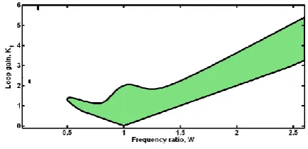
The locking range of the first-order TDTL with a nominal phase shift / 2 is
shown in Figure 2.
Figure2 The locking range of first-order TDTL. K1G ω1 o and W ω / ω o .
The second-order TDTL, shown in Figure 3, uses a proportional accumulation
digital filter whose transfer function D z
is 1
1 2/ (1 )
D z G G z (17)
y(t)
Time Delay τ and HoldSample
[image:8.595.187.404.288.393.2]Sample and Hold Digital Controlled Oscillator (DCO) Digital Filter Phase Detector Arctan(x/y) x(t) x(k) y(k) Input Signal e(k) c(k)
Figure 3 Block diagram of the second-order TDTL architecture.
whereG1and G2 are positive constants. Using equations (13) and (17), the difference
[image:8.595.177.429.492.646.2]Page 8 of 29
' '
1 1
2 2 1 1
k k k rK e k K e k
(18)
wherer 1 G G2/ 1and
' '
1 1
K K.
Following similar approach to that in (Hussain et al., 2001) with a fixed-point
analysis as in (Al-Araji et al., 2004) the locking range of the second-order TDTL,
Figure 4, may be written as
1
4
0
1 r
o
K W sin W
(19)
3. First- and Second-order TDTL Simulation Results
The performance of the first-order loop, presented in Figure 1, was
extensively tested using input signals with sudden frequency changes relative to the
free running frequency of the DCO. When the change in the input frequency makes it
higher than that of the DCO, the change will be represented as a positive step,
otherwise it is indicated as a negative step. For testing purposes, the time delay and
the DCO free running frequency values have been chosen so that the initial phase lag
[image:9.595.182.409.483.593.2]parameter ψoω τ π / 2o and the gainK1G ω1 o1.
Figure 4 The second-order TDTL locking range (r =1.2 K1G1o and W o/ ).
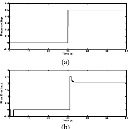
Figure 5 shows the effect of applying a positive input frequency step of 0.5 V (
o in
W ω / ω 0.667) to the loop, whilst, Figure 6 shows the results of applying a
negative input step of -0.3 V that corresponds to W ω / ω o in 1.428. As can be seen
steady-Page 9 of 29 state within the time of few samples. However, this time may not be acceptable for
some applications requiring fast acquisition speeds. Hence, increasing the acquisition
speed is an important goal for a PLL engineer. An additional goal is to
minimise/eliminate the finite phase error of the first-order TDTL loop. Albeit, this
goal can be achieved using a second-order loop, this will be at the cost of degradation
in the acquisition performance and the locking range as will be demonstrated below.
(a)
(b)
Figure 5 (a) A 0.5 V input step and (b) first-order TDTL phase-error response.
Similar tests were also carried out to evaluate the performance of the
second-order TDTL system of Figure 3. The results of the phase error tests are shown in
Figure 7 and 8, which show that the steady-state error of the second-order loop
converges to zero. Clearly, improving the loop locking speed is desirable as some
applications require fast synchronization.
[image:10.595.199.411.239.451.2] [image:10.595.201.411.637.751.2]Page 10 of 29 (b)
[image:11.595.200.411.76.182.2]Figure 6 (a) Negative input step of -0.3 V and (b) phase error response of the first-order TDTL.
Figure 7 Phase error response of the second-order TDTL for a positive input frequency step of 0.3 V.
Figure 8 Phase error response of the second order TDTL for a negative input frequency step of -0.3 V.
4. Improvements to the Original TDTL
The analytical system models and the simulation results given earlier for the
first- and second-order TDTLs show that the system has some constraints, which
when overcome, the performance of both loops will be enhanced. The main system
limitations that need to be addressed are:
The nonlinearity in the first- and second-order TDTLs. This is attributed to
having a fixed-time delay unit that results in different phase shifts for different
[image:11.595.200.408.247.335.2] [image:11.595.200.410.384.475.2]Page 11 of 29
The second-order TDTL has a rather restricted locking range which can be
extended.
The first-order TDTL has relatively low acquisition speed, which can be
improved.
Phase-error convergence to zero of the second-order TDTL phase error tends to
take a relatively long time.
The non-zero steady-state phase error of the first-order TDTL is an obvious
disadvantage.
The subsections below propose new TDTL system architectures that overcome
the above limitations of the original TDTL.
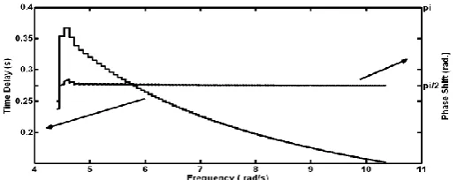
4.1TDTL with new linear phase detector
The fixed-time delay is the primary source of nonlinearity and it severely
influences the locking range of the TDTL system. The idea of eliminating this
nonlinearity problem by substituting the fixed-time delay block with a variable time
delay unit has been proposed in the paper (Al-Qutayri, Al-Araji, Al-Kharji Al-Ali,
and Anani, 2009). In this article, an improved TDTL equipped with a linearized phase
detector (TDTL-LPD) is proposed as shown in Figure 9. It incorporates a controller
for phase linearization as well as a variable ‘adaptive’ time delay block.
The phase linearization controller in the TDTL-LPD estimates the error caused
by fluctuations in the frequency of the incoming signal during the time the loop is in
locked condition. This estimate is then used to compensate for the non-linear changes
in the phase by fine-tuning the adaptive time delay unit in order to preserve the
quadrature relationship between the input signal y t and its quadrature version x t .
The idea of the TDTL-LPD can be explained by examining the phase shift
Page 12 of 29
(20)
Where (rad) is the phase shift, (rad/s) is the frequency and (s) is the time delay
initiated by the variable time-delay unit.
y(t)
Variable delay
Sample and Hold
Sample and Hold Digital Controlled
Oscillator (DCO)
Digital Filter
Phase Detector Arctan(x/y)
x(t) x(k)
y(k) Input
Signal
e(k) c(k)
Phase Linearization
[image:13.595.182.423.159.285.2]Controller
Figure 9 Architecture of the conventional first order TDTL-LPD.
The phase linearization controller in the TDTL-LPD compensates for changes in the
input frequency to yield a fixed phase shift (rad) while the system is working inside
its nominal locking range. Consequently, variations in the input signal frequency will
be counteracted by a suitable value of delay generated by the controller in order to
uphold a / 2 (rad) phase shift. As shown in equation (21), for any rise in the incoming
signal frequency, there will be a reduction in the time delay to keep the phase shift
fixed at / 2 (rad) as demonstrated in Figure 10.
2
2
f rad (21)
A comparison between the phase detector characteristics of the conventional
TDTL and the TDTL-LPD is depicted in Figure 11. The TDTL has nonlinear parts
while the TDTL-LPD follows a straight line, which indicates the nonlinearities have
Page 13 of 29 Figure 10 Variation in the required time delay with the input signal frequency to
preserve a phase shift of / 2 (rad).
Figure 11 Characteristics the TDTL-LPD and TDTL phase detectors.
Preserving the phase shift at the value of / 2(rad) , means that the phase shifted
incoming signal x k
, of equation (4), can be expressed as ( )
2
o o
x k Asin t k k Acos t k k (22)
This is similar to the DTL in (Gloria, Grosso, Olivieri, and Restani,1999), therefore,
the discretized signals generated by the samplers are
1
0
sin ( ) ok ( )
i
y k A k c i
(23) then 1
0
cos ( ) ok ( )
i
x k A k c i
(24) Consequently, both (23) and (24) can be re-written in terms of the phase error as
sin
y k A k (25)
and
cos ( )
x k A k (26)
Page 14 of 29
tan 1 sin ( ) k ( )
e k f f k
cos k (27)
where f [ mod 2 ] . Consequently, the first-order TDTL's locking range
(Jae, and Chong,1982; Al-Qutayri et al., 2009), can be given as
2 2
1
( )
2
2 1 2
sin( ) 2
sin sin
W K W
(28)
1
2
2 1 2
( 2 cos 2 cos( 2 )
W K W
(29)
which can be simplified as
1
2 1W K 2W (30)
In case of the second-order TDTL-LPD, equation (19) may be expressed as
1 4
0
1 r 2
K W sin
(31)
1 4 0 1 r K W
(32)
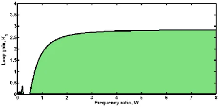
Both first- and second-order TDTL-LPD locking range with a fixed phase shift of
/ 2
(rad) is shown in Figure 12 and 13. As demonstrated below, the TDTL-LPD
response outperforms that of the conventional TDTL.
Figure12 First order TDTL-LPD locking rang,K1G1o, W o/ and / 2(rad).
Figure13 Second-order TDTL-LPD locking range with (r=1.2),K1G1o,W o/ and
/ 2
Page 15 of 29 The responses of first-order TDTL-LPD and the TDTL to the injection of positive and
negative frequency steps are shown in Figure 14 and 15 respectively. It can be seen
from the figures that the TDTL-LPD requires less number of samples to achieve locking
state compared to the TDTL.
(a)
(b)
Figure14 Phase error responses for positive input frequency step of 0.3 V (a) first-order TDTL-LPD and (b) first-first-order TDTL,K1G1o,W o/ and / 2(rad).
(a)
(b)
Page 16 of 29 Both Figures 14 and 15 demonstrate the enhancement in the acquisition time of
the first-order TDTL-LPD architecture, which is obtained by using a fixed phase shift
value for all incoming signal frequencies, which consequently linearizes the phase
detector.
The evaluation of the response of the second-order TDTL-LPD followed a
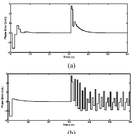
similar approach to that of the first-order. The responses of the TDTL-LPD and the
[image:17.595.187.406.296.520.2]TDTL to the application of positive and negative frequency steps are shown in
Figure 16 and 17 respectively.
(a)
(b)
Figure16 Phase error response for positive input frequency step of 0.4 V (a) second-order TDTL-LPD and (b) second-second-order TDTL, / 2(rad), r =1.2 and K11.
[image:17.595.187.405.587.686.2]Page 17 of 29 (b)
Figure 17 Phase error response for negative input frequency step of -0.3 V (a) second-order TDTL-LPD and (b) second-order TDTL, / 2(rad), r =1.2 and K11.
The locking range performance of the TDTL-LPD was tested and compared to
that of the original TDTL. Figure 18 shows an example of such tests with a frequency
step of 0.6 V. As can be seen, in Figure 18a, the original TDTL goes out of lock while
in Figure 18b the TDTL-LPD attains the locking condition. A moderate improvement
is achieved in the acquisition time of the second-order TDTL-LPD in comparison with
the conventional TDTL. This will be investigated in detail in the following section.
(a)
(b)
Page 18 of 29 4.2 Second-order TDTL with Improved locking range and acquisition
As stated earlier and based on the responses in Figures 16 and 17, the acquisition
speed of the second-order TDTL-LPD needs to be improved further. An improvement
in the sampling will enhance the loop acquisition due to the accumulation path nature
of the digital loop filter. This results in speeding up the time to reach the zero
steady-state as proposed in the TDTL with wide locking range and fast acquisition
(TDTL-WFA) architecture (Al-Araji, Al-Kharji Al-Ali, Al-Qutayri, Anani, and Ponnapalli
2010).
In order achieve faster acquisition the DCO unit is revised as illustrated in
Figure 19. The idea is to boost the free running frequency of the DCO by a factor ‘M’,
which is then used to accelerate the response of the loop digital filter. As shown in
Figure 19, the free running frequency of the DCO is subsequently divided by the ‘M’
so as to preserve the loop sampling rate. The remaining blocks of Figure 19 are similar
to the original TDTL-LPD. The performance of the second-order TDTL-LPD was
compared with that of the improved second-order TDTL-WFA through an extensive
set of tests. In those tests the oscillator's free running frequency was doubled by setting
M=2.
DCO y(t)
Variable Time Delay
Phase Linearization
Controller
Digital Filter
Phase Detector Arctan(x/y)
x(t) x(k)
y(k) Input
Signal
÷ M
Digital Controlled
Oscillator (DCO To/M)
Sample and Hold Sample and Hold
Figure19 Block diagram of the TDTL-WFA system.
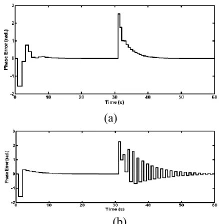
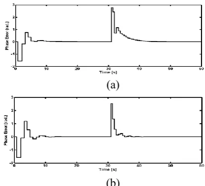
As in previous cases, the tests involved subjecting the loop to the same
Page 19 of 29 and comparing their responses. The results of the TDTL-WFA response show that it
outperforms the TDTL-LPD. The responses of both loops to a positive frequency step
of 0.4 V and a negative frequency step of -0.3 V, while the loops are inside their locking
range, are shown in Figures 20 and 21 respectively. In both cases, the TDTL-WFA
required considerable less number of sample times compared to the TDTL-LPD to
converge to zero steady-state phase error and hence achieves full locking.
As can be expected, the acquisition speed of the TDTL-WFA can be improved
by increasing the value of ‘M’. This is demonstrated in Figure 22 by increasing M from
2 to 4 while applying a frequency modulated (FM) input signal, which shows that the
peak of the error for M=4 is nearly half that for M=2.
(a)
[image:20.595.192.400.349.537.2](b)
Figure 20 Phase error responses for positive input frequency step of 0.4 V (a) second-order TDTL-LPD and (b)second-second-order TDTL-WFA, / 2(rad), r =1.2 and K11.
Page 20 of 29 (b)
Figure 21 Phase error responses for negative input frequency step of -0.3 V (a) second-order TDTL-LPD and (b) second-order TDTL-WFA, / 2(rad)., r =1.2 and
1 1
K .
Figure 22 Phase error response of the TDTL-WFA as M is doubled with an FM input signal, / 2(rad), r =1.2 and K11.
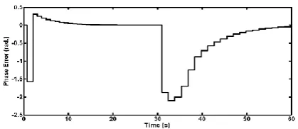
4.3 An adaptive first-order TDTL with zero phase error (ATDTL-ZPE)
An adaptive TDTL with zero steady-state phase error (ATDTL-ZPE) (Al-Kharji
Al-Ali, Al-Araji, Anani, Al-Qutayri, and Ponnapalli 2010) that overcomes the non-zero
steady-state error of the first-order TDTL is examined in this section. In addition to
eliminating the non-zero phase error, the architecture extends the loop locking range.
Compared to the original TDTL, the ATDTL-ZPE shown in Figure 23
incorporates a Frequency Estimator Controller (FEC) and an Adder block. The main
concept behind this architecture is the use of these blocks to initialize the loop DCO to
generate a frequency that matches that of the incoming signal. Hence, the new blocks
in the ATDL-ZPE enable frequency tracking, as the DCO samples the input signal at
its frequency and that frees the loop to work on tracking and correcting the phase error
generated at the arctan phase detector output. This process enables the reduction of the
first-order loop steady-state phase error to zero. An added advantage of this
[image:21.595.194.402.222.317.2]Page 21 of 29 transparent translation or shift process of the loop locking range to the anticipated
frequency range. To linearize its phase, the ATDTL-ZPE shown in Figure 23 uses a
variable delay block as the case in the TDTL-LPD (Al-Qutayri et al., 2009).
As can be seen in Figure 24, the FEC block of the ATDTL-ZPE consists of a
derivative function, subtractor block, gain block, low-pass filter, multiplier, and a
constant reference value of the DCO free running frequency (F0). The delayed signal
is multiplied with the signal generated by the derivative block. The signal that results
from this multiplication is fed to the low-pass filter which detects its envelope.
The DCO is initialized by the FEC, Figure 25, so that the incoming signal is
sampled at a rate that equals its frequency but with a different phase. Subsequently the
loops works at reducing this phase error, which manifests itself at the output of the
arctan, phase detector.
y(t) Variable Delay Digital Controlled Oscillator (DCO) Digital Filter Phase Detector Arctan(x/y) x(t) x(k) y(k) Frequency Estimator Controller Adder Input Signal Phase Linearization Controller Sample and Hold Sample and Hold
Figure23Architecture of the ATDTL-ZPE.
Derivative Gain (1/(2*pi)) Low Pass Filter y(t) x(t) Fo Value +
-Figure24 block diagram of the Frequency estimator controller.
The locking range of the AZPE is similar to that of the first-order
Page 22 of 29 frequency the ATDTL-ZPE has the ability to swiftly change the locking range to the
exact frequency. As a result, it will constantly operate with W=1 keeping K1 at the
initial value of 1. However, K1 must be maintained inside the interval 0 < K1 < 2 for
the loop to remain locked.
As in previous cases, the performance of the ATDTL-ZPE was compared to that
of the original first-order TDTL by subjecting both loops to the same input frequency
[image:23.595.188.401.433.758.2]steps. The response of both loops to a positive frequency step of 0.3 V is illustrated in
Figure 25. In addition to the input frequency step, Figure 25 shows the output of the
carrier estimator controller, and the phase errors of both loops. It is evident from Figure
25 that the ATDTL-ZPE achieves the desired zero steady-state phase error. A similar
test was performed using a negative step of -0.3 V and the results are shown in Figure
26. In both Figures 25 and 26, the ATDTL-ZPE achieves faster acquisition time
compared to original TDTL. As indicated earlier this is due to the initialization process.
(a)
(b)
Page 23 of 29 Figure 25 First order TDTL phase-error to positive frequency step input 0.3 V (a)
FEC, (b) ATDTL-ZPE and (c) TDTL, / 2(rad). and K11.
(a)
(b)
[image:24.595.187.405.132.460.2](c)
Figure 26 First order TDTL response to negative frequency step input -0.3 V, (a) FEC, (b) ATDTL-ZPE and (c) TDTL, / 2(rad).and K11.
5. Noise, Jitter and BER Performance Tests
The effects of noise on the operation of the different TDTL architectures
presented above are presented in this section. The noise performances are assessed
using the probability density function (pdf). In the assessment, the input signal is
assumed to have been corrupted by a zero mean additive white Gaussian noise (AWGN)
which has two-sided power spectrum density of Gnw f n / 2o (Peyton, and Peeblesand,
1993; Haykin, and Moher, 2009; Skiller, and Huang, 2000). Therefore, autocorrelation
may be obtained using the inverse Fourier Transform of Gnw
f Gnw(f)as
oPage 24 of 29
R τ 0for τ 0 , hence any two samples of this form of noise are uncorrelated and
therefore, they are statistically independent (Hussain, 2005; Pomalaza-Raez, 1988;
Mehrotra, 2002; Ibrahim, and Hamadamin, 2006; Al-Kharji Al-Ali, Anani, Al-Araji,
Al-Qutayri, and Ponnapalli, 2012).
Figures 27 and 28 show some specimens of the extensive simulation results. In
Figure 27, the TDTL-LPD outperforms the original TDTL for an SNR over 5 dBs. This
is due to the fact that the use of the fixed delay block, in the TDTL, increases the
phase-detector nonlinearity as the SNR increases.
The results in Figure 28 demonstrate that the performance of the ATDTL-ZPE
surpasses that of the TDTL-WFA due to the fact that the ATDTL-ZPE is only used for
phase synchronization as explained earlier. Furthermore, Figure 28 demonstrates that
the ATDTL-ZPE and the TDTL-WFA outperform the second-order TDTL for SNR
above 5 dBs. This is because when the TDTL-WFA is subjected to a fairly noisy
environment, the fast acquisition characteristic will produce a reverse effect in
delivering a fast settling time to the steady-state condition. However, since the
ATDTL-ZPE makes use of the FEC to accomplish frequency tracking, the loop is only required
to attain phase synchronizing.
In very noisy environments i.e. when the SNR is less than 5 dBs, the FEC block
cannot deliver the exact frequency value required by the TDTL loop and this results in
degraded noise performance. Figure 29 illustrates the effect of noise on the jitter
performance. From the figure, the ATDTL-ZPE gives the best performance while the
original second-order TDTL gives the worse jitter. The reasons for these variations are
the additional blocks that were introduced to the ATDTL-ZPE, TDTL-WFA and
Page 25 of 29 (a)
(b)
[image:26.595.193.399.70.366.2](c)
Figure 27 Noise performance od the first order architectures (a) SNR=5 dB (b) SNR=10 dB and (c) SNR=15 dB.K11 and frequency step of 0.1 V.
(a)
(b)
(c)
[image:26.595.190.403.416.723.2]Page 26 of 29 (a)
[image:27.595.181.409.72.276.2](b)
Figure 29 Variation of the Jitter with SNR (a) linear scale and (b) Logarithmic scale,
1
K 1 and step inputs of 0.1 V.
The performance of all the proposed TDTL based architectures, including the
original TDTL, was evaluated under slow as well as fast fading channel conditions. In
the case of slow fading channels, the performance of the various architectures was
found to be almost similar. This is an expected result because under slow fading, the
particular system loop will only need to deal with relatively small changes in the input
signal. However, under fast fading conditions the performance of the improved TDTL
architectures showed noticeable improvement compared to the original TDTL. This is
due to the improved characteristics of the proposed architectures, such as wider locking
range and higher acquisition speed, which enable them to cope with the relatively larger
changes in the input signal. The improvement under fast fading conditions is
demonstrated by the BER results in Figure 30. The BER performance was evaluated
using a constant envelope orthogonal frequency division multiplexing (CEOFDM) with
Page 27 of 29 Figure 30 BER performance of different TDTL enhanced architectures for CEOFDM
modulations under fast varying channel.
6. Conclusions
This paper presented a variety of system architectures to overcome some of the
limitations of the original first- and second-order TDTL systems. The proposed
TDTL-LPD overcame the nonlinearity associated with the original TDTLs by incorporating a
phase linearization block. The TDTL-WFA system resolved the acquisition speed
limitation of the second-order TDTL-LPD through the introduction of a modified DCO
that over drives the digital loop filter. A widening of the lock range was achieved as
an additional advantage of this process by seamlessly shifting the TDTL lock range to
a specific frequency and hence preserving locking by maintaining the loop operating
frequency at W=1. The non-zero phase error convergence of the first order TDTL was
resolved by the ATDTL-ZPE, which has an adaptive mechanism targeted at solving
this problem. The ATDTL-ZPE also achieved wider locking range than the original
TDTL.
All the proposed systems architectures, LPD, WFA and
TDTL-ZPE, achieved significantly better overall performance than the original TDTL when
evaluated under noisy conditions. Each of the said architectures was targeted at
improving a particular aspect of the system performance. Consequently, the choice of
Page 28 of 29 that demand high acquisition speeds, the TDTL-WFA system can be employed.
However, the ATDTL-ZPE delivers best noise performance. Finally, improved
linearity was the objective of the TDTL-LPD. The performance of all TDTL
architectures was assessed under fast fading channel conditions. The results
demonstrated that the modified architectures provided improved BER performance
over the original TDTL architecture.
References
Guan-Chyun H., and Hung, J. C. (1996).Phase-locked loop techniques: A survey, IEEE Transactions on Industrial Electronics, 43, 609-615.
Lindsey W. C., and Chak M. C. (1981).A survey of digital phase-locked loops. Proceedings of the IEEE, 69: 410-431.
Gardner, F.M., (3rd Ed.) (2005).Phase lock Techniques. New York, USA: John Wiley.
Terng-Yin, H., Bai-Jue, S. and Chen-Yi, L. (1999),An all-digital phase-locked loop (ADPLL)-based clock recovery circuit. IEEE Journal of Solid-State Circuits; 34, 1063-1073.
Best, R.E. (2007), Phase-Locked Loops: Design, Simulation, and Applications, New York: McGraw-Hill.
Crawford, J.A. (2007). Advanced Phase-Lock Techniques. USA: Artech House. Pearce, J.M., Al Zahawi, B. A. T., and Shuttleworth, R. (2001). Electricity generation
in the home: Modelling of single-house domestic combined heat and power.IEE Proceedings - Science, Measurement and Technology. 148, 5, 197-203
Pearce, J.M. Al Zahawi, B. A. T. Auckland, D. W and Starr, F. (1996). Electricity generation in the home: An evaluation of single-house combined heat and power,’
IEE Proceedings - Science, Measurement and Technology, 143, 6, 345-350. Anani, N., Al-Kharji Al-Ali, O., Ponnapalli, P., Al-Araji, S. R., and Al-Qutayri, M.
(2012a).Synchronization of A single-phase photovoltaic generator with the low-voltage utility grid. Transactions of the Journal of solar energy engineering of the American Society of Mechanical Engineers, 134,1, 0110071-78, doi:10.1115/1.4005337.
Anani,N., Al-Kharji Al-Ali,O., Ponnapalli, P., Al-Araji, S., and Al-Qutayri, M. (2012b).Synchronization of a renewable energy inverter with the grid, American Institute of Physics: Transactions of the Journal of Renewable and Sustainable Energy, 4, 4, 1941-7012.
Jae, L., and Chong, U. (1982).Performance Analysis of Digital Tanlock Loop.IEEE Transactions on Communications, 30, 2398-2411.
Hussain, Z. M., Boashash, Hassan-Ali, B. M., and Al-Araji, S. R. (2001), A time-delay digital tanlock loop, IEEE Transactions on Signal Processing, 49, 1808-1815. Al-Araji, S. R., Al-Qutayri, M. A., and Al-Moosa, N. (2004). Digital Tanlock Loop
with Extended Locking Range using Variable Time Delay. The 47th Midwest Symposium on Circuits and Systems (MWSCAS), 161-164.
Page 29 of 29 Osbornen, H. C.(1980b), Stability Analysis of an Nth Power Digital Phase-Locked Loop-Part II: Second- and Third-order DPLLs. IEEE Transactions on Communications; 28: 1355 - 1364.
Al-Qutayri, M. A., Al-Araji, S. R., Al-Kharji Al-Ali, O., and Anani, N. A. (2009). Time delay digital tanlock loop with linearized phase detector, 16th IEEE International Conference on Electronics, Circuits, and Systems (ICECS); 555 - 558.
Gloria De, Grosso, D., Olivieri, M., and Restani, G. A novel stability analysis of a PLL for timing recovery in hard disk drives. IEEE Transaction of Circuits System I,
Fundamental. Theory and Applications 1999;46:1026-1031.
Al-Araji, S. R., Al-Kharji Al-Ali, O., Al-Qutayri, M. A., Anani, N., and Ponnapalli, P. V. S. (2010), Improved performance second order time delay digital tanlock loop.
IEEE Sarnoff Symposium;1 - 5.
Al-Kharji Al-Ali, O., Al-Araji, S. R., Anani, N. A., Al-Qutayri, M. A. and Ponnapalli, P. V. S. (2010), Adaptive TDTL using frequency and phase processing technique.
10th International Conference on Information Sciences Signal Processing and their Applications (ISSPA),530-533.
Peyton, Z. and Peeblesand, Jr. (1993), Probability, Random Variables, and Random Signal Principles. New York:McGraw-Hill.
Haykin, S. and Moher, M. (2009). Communication Systems. New Jersey: John Wiley. Skiller, G. and Huang, D. (2000). The stationary phase error distribution of a digital
phase-locked loop. IEEE Transactions on Communications,48:925-927.
Hussain, Z. M. (2005). Performance of the Time-Delay Digital Tanlock Loop as PM Demodulator in Additive Gaussian Noise. Proceedings of IEEE TENCON Region; 1-6.
Pomalaza-Raez, C.A. (1988). Noise analysis of a digital tanlock loop, IEEE Transactions on Aerospace and Electronic Systems.24: 713 -718.
Mehrotra, A. (2002). Noise analysis of phase-locked loops. IEEE Transactions on Circuits and Systems I: Fundamental Theory and Applications; 49, 1309-1316. Ibrahim, M. A., and Hamadamin, J. A. (2006). Noise Analysis of Phase Locked Loops,
5th Proceeding WSEAS International Conference on Telecommunication and Information. 479-484.
Al-Kharji Al-Ali, O., Anani, N., Al-Araji, S., Al-Qutayri,M., and Ponnapalli, P. (2012). Digital tanlock loop architecture with no delay. International Journal of Electronics, 99,179-195, DOI:10.1080/00207217.2011.623271.
Al-Kharji Al-Ali, O., Anani, N., Al-Qutayri,M., and Al-Araji, S., (2012). Analysis and optimization of the convergence behaviour of the single channel digital tanlock loop. International Journal of Electronics, 0, 1-13.