Fabrication of Photocatalytic TiO2 Films on Pure Aluminum Plates
7
0
0
Full text
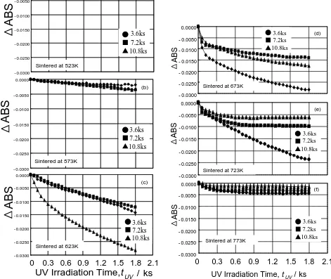
(2) 940. S. Ikeno et al.. H 2O. ROH OR H ROH HO Ti O OR ROH. H2O. OR Ti. OR. OH HO. OR. : hydrophobic solvent of benzene. Ti. OR O. Ti. OH. OR. OR. Hydrophilic group. Hydrophobic group. Fig. 1 Schematic illustration of titanate oligomer (titanium oxide cluster).. of the oxide layer using Mg–Kα X-ray source (1253.6 eV, PHI Model 04–151, Perkin-Elmer, USA) at 10 kV and 40 mA. A double-pass cylindrical mirror analyzer (PHI Model 15255G, Perkin-Elmer, USA) was operated at a sweep rate: of 0.02–1.0 eV/s and pass energy of 50–100 eV. 2.3 Preparation and observation of X-TEM samples X-TEM samples were prepared by foucused ion beam (FIB) milling and mechanical extraction, which is refered to as “the picking-up technique”,14) as follows. Platinum was deposited on the TiO2 -coated Al plate by an ion-coater to create an electrically conductive layer in preparation for FIB milling. A strip of carbon was then deposited on the surface to protect the TiO2 nano-film in the FIB chamber, and the section was milled out by milling 10 µm × 3 µm × 10 µm holes on either side of the section, creating a narrow (200 nm) wall between the holes. The sample was then tilted by about 60◦ in order to mill the bottom of the wall, and one side connecting the wall to the TiO2 -coated Al plate was also milled. A small tip of the cross-section of the TiO2 -coated Al sample was produced in this way, and was picked up using a glass probe, picked up and mounted on a carbon film supported by copper grid. The thickness of this tip was estimated to be less than 200 nm accourding to its convergent beam electron diffraction (CBED) pattern obtained by TEM (EM-002B, Topcon, Japan) at 200 kV. These samples are somewhat thick for highresolution TEM observation but sufficient to construct bright field images and elemental maps by EFTEM. The EFTEM (4010T, JEOL, Japan) was used with GIF-200 energy-filter (Gatan Inc., USA) and operated at 400 kV. Elemental maps were taken using three windows under the conditions listed in Table 1. 3. Results and Discussion 3.1 Effect of sintering temperature Figure 2 shows the change in ∆ABS with UV irradiation time for samples sintered at temperature between 523 and 773 K, indicating the photocatalytic activity of the samples. At the lowest sintering temperature of 523 K (Fig. 2(a)), ∆ABS remains virtually unchanged, only decreasing slightly after extended irradiation time. Here, we can define negligiblephotocatalytic activity as ∆ABS smaller than −0.005, low activity as smaller than −0.01, and acceptablephotocatalytic activity as larger than −0.01. Hence, this sample exhibits. Table 1 Details of the acquisition of elemental maps for X-TEM sample.. Pre-edge 1 (eV) Pre-edge 2 (eV) Post edge (eV) Slit width (eV) Acquisition time (s). Ti. O. Al. 416 436 456 10 30. 497 517 532 10 30. 1470 1520 1560 30 60. little photocatalytic activity. The sample sintered at 573 K shown in Fig. 2(b) exhibited a greater response, yet was still relatively constant. The ∆ABS of samples prepared at 623 and 673 K in Figs. 2(c) and (d) decreased remarkably with irradiation time, and exhibit the optimalphotocatalytic activity with respect to sintering time and irradiation time. At higher temperatures in Figs. 2(e) and (f), the photocatalytic activity again decreased to quite low values. The sample sintered at 673 K for 3.6 ks is the most appropriate specimen with respect to both the shortest sintering time and the optimal photocatalytic activity. 3.2 Effect of lifting-up speed In general, the photocatalytic activity of TiO2 is controlled by its crystal structure, and highphotocatalytic activity is obtained at a critical temperature that yields an anatase structure.15) X-ray diffraction measurements were performed in order to detect the peaks of anatase structure, and low peaks of anatase structure of 25.3◦ ({101}) and 38.6◦ ({112}) were obtained from the samples sintered at 673 K as shown in Fig. 3(a). A peak of 25.3◦ was just used to identify for anatase structure, because a peak of 38.6◦ for an anatase structure is more weaker than 25.3◦ , which could not be confirmed actually, and a peak of 38.4◦ for aluminum ({111}Al ) superimposes with a peak of 38.6◦ for an anatase structure. This suggests that the TiO2 film was probably too thin. The lifting-up speed V was then controlled so as to vary the thickness of the TiO2 films. The results for the samples sintered at 673 K for 3.6 ks are shown in Fig. 4. Thephotocatalytic activity of the sample lifted up at 0.248 mm/s was higher than that lifted up at the original V of 0.165 mm/s, however, higher liftingup speeds produce films with the samephotocatalytic activity as that of the original film. The film thickness appears to increase with lifting-up speed up to a critical speed Vc as a result of the solidification of the precoursor solution before.
(3) Fabrication of Photocatalytic TiO2 Films on Pure Aluminum Plates. 941. 0.0000. (a). ABS. - 0.0050 - 0.0100. 0.0000. 3.6ks 7.2ks 10.8ks. - 0.0200 - 0.0250. Sintered at 523K. - 0.0100. (d). - 0.0150 - 0.0200. - 0.0300 0.0000. - 0.0250. (b). Sintered at 673K. - 0.0300. - 0.0050. 0.0000. (e). - 0.0100. - 0.0050 - 0.0150. 3.6ks 7.2ks 10.8ks. - 0.0200. ABS. ABS. 3.6ks 7.2ks 10.8ks. - 0.0050. ABS. - 0.0150. - 0.0100. 3.6ks 7.2ks 10.8ks. - 0.0150 - 0.0200. - 0.0250. Sintered at 573K. - 0.0250. - 0.0300 0.0000. Sintered at 723K - 0.0300. ABS. (c). 0.0000. - 0.0050. (f) - 0.0050. ABS. - 0.0100 - 0.0150. 3.6ks 7.2ks 10.8ks. - 0.0200 - 0.0250. Sintered at 623K. - 0.0100 - 0.0150 - 0.0200 - 0.0250. Sintered at 773K. 3.6ks 7.2ks 10.8ks. - 0.0300. - 0.0300. 0. 0.3 0.6 0.9 1.2 1.5 1.8 2.1. UV Irradiation Time,t UV / ks. 0. 0.3 0.6 0.9. 1.2 1.5 1.8. 2.1. UV Irradiation Time, t UV / ks. Fig. 2 Changes in ∆ABS with UV irradiation time (tUV ) of samples sintered at (a) 523 K, (b) 573 K, (c) 623 K, (d) 673 K, (e) 723 K and (f) 773 K.. running back into the bath. Here, Vc appears to be around 0.248 mm/s, above which the morphology of film surface produced is thought to become wavy and non-uniform, resulting in a reduction in photocatalytic activity. The peak assigned to the anatase structure of 25.3◦ becomes intense with increasing V , particularly for the sample lifted up at 0.408 mm/s. It is seems that the absence of anatase peak is attributable to the weak response of the thin layer. 3.3 Suitable conditions to form TiO2 films We have therefore clarified that there is a critical lifting-up speed, and a clear relationship between sintering temperature and sintering time for the fabrication of TiO2 films on aluminum plates with respect to photocatalytic activity. Figure 5 shows a summary of the suitable fabrication conditions for this system. Open and closed circles, and open triangles show that optimal, acceptable and poorphotocatalytic activities of TiO2 films. There is a region of sintering conditions that are suitable for forming TiO2 films with highphotocatalytic activity on aluminum plate. The anatase crystallization conditions are also shown. The surface morphologies of TiO2 films, as. Fig. 3 X-ray diffraction patterns for TiO2 films on Al plates sintered at 673 K for 3.6 ks and lifting-up speed (V ) of (a) 0.165, (b) 0.248, (c) 0.323 and (d) 0.408 mm/s.. obtained SEM, are shown in Fig. 6 for samples sintered at 623, 673 and 723 K for 3.6 ks. The samples sintered at 623.
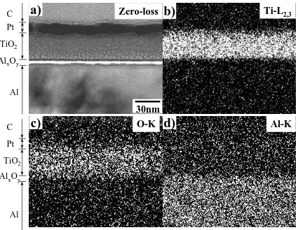
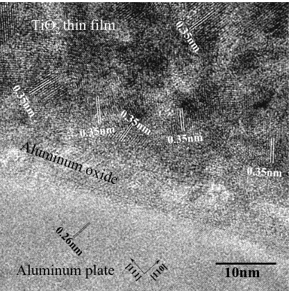
(4) ABS. 942. S. Ikeno et al.. 0.0000 - 0.0050 - 0.0100 - 0.0150 - 0.0200. (a). 0.165 mm/s 0.248 mm/s 0.323 mm/s 0.408 mm/s. - 0.0250 - 0.0300 - 0.0350 - 0.0400 Sintered at 673 K for 3.6 ks - 0.0450 0 0.3 0.6 0.9 1.2. 1.5. 1.8. 2.1. UV Irradiation Time, t UV / ks. Sintering Temperature, T/ K. Fig. 4 Changes in ∆ABS of samples formed at several lifting-up speeds (V ) prior to sintering at 673 K for 3.6 ks.. 823 773 723 673 623 573 523. 200. m. : optimal : acceptable : poor. Anatase structure. (b) Optimalrange range excellent. Non-crystalline. 3.6. 7.2. 10.8. Sintering Time, t / ks. 1mm. Fig. 5 Relationship between sintering temperature and sintering time with respect to photocatalytic activity.. and 723 K exhibit scratches and peeling, whereas the sample sintered at 673 K had a smooth surface. This is not an essential reduction of photocatalytic activity of samples, but, it is important for industrial applications of this advanced sol-gel method and ∆ABS method, which is significantly affected the surface condition of samples on the response for the change in ∆ABS. 3.4 Observation of X-TEM sample The morphology and TEM image of the X-TEM is shown in Figs. 7(a) and (b). The central dark line in Fig. 7(b) was the TiO2 film, the lower layer was the aluminum plate, and the upper layer was the protective carbon. The Pt layer was located between the carbon and TiO2 . Figure 8(a) shows a zero-loss image of the area marked in Fig. 7(b). The interface between the Pt-layer and the TiO2 film was very flat. No cracks were observed between TiO2 nano-film and aluminum plate, although a layer of unknown composition did exist between them. Figures 8(b) to (d) are elemental maps of the X-TEM sample obtained by EFTEM to confirm the chemical composition of each layer. The TiO2 film was almost 30 nm thick, and can be seen more clearly than in the zero loss image. This thickness of 30 nm is consistent with that measured by atomic force microscopy in a previous study.8) As region of Ti was clear in Fig. 8(b) and does not extend into the underlying Al, indicating that Ti did not diffuse into the aluminum plate when the sample is sintered. As the TiO2 film overlaps with the unknown-layer in the O-map, the unknown-layer is. (c). 1mm Fig. 6 SEM images of surface morphologies of samples sintered for 3.6 ks at (a) 623, (b) 673 and (c) 773 K.. expected to be Alx O y . The Al of the aluminum plate also overlaps this Alx O y region in the Al-map. Figure 9 shows an HRTEM image of the TiO2 film. Lattice fringes of 0.29 nm can be seen, corresponding to the {111} plane of aluminum, and lattice fringes in agreement with the spacing of the {101} plane of anatase structure.16) There are also regions with different orientations of fringes, with mean size about 12 nm. From this observation, the TiO2 film is considered to be finely crystalline with a mean crystal size of 12 nm. The Alx O y layer.
(5) Fabrication of Photocatalytic TiO2 Films on Pure Aluminum Plates. 943. Fig. 7 Morphology of X-TEM sample. (a) Optical micrograph and (b) bright-field TEM image.. a). C. Zero-loss. b). Ti-L2,3. d). Al-K. Pt TiO2 AlxOy. Al. 30nm. c). C. O-K. Pt TiO2 AlxOy. Al Fig. 8 Results of EFTEM observation. (a) Zero-loss image, (b) Ti–L2,3 , (c) O–K and (d) Al–K elemental maps.. is amorphous like structure and approximately 5 nm thick. The interface between the TiO2 and Alx O y could not be seen, nor can that between aluminum plate and Alx O y . It is considered that adhesion of these layers is consistently on the atomic scale. It is well known that aluminum plates have oxide layer on their surface and they are formed by the natural oxidation in the atmosphere or by anodic oxidation.17, 18) To confirm the formation of the oxide, the chemical composition. of the oxide layer was examined by XPS for an aluminum plate prepared by electrolytic polishing prior to sintering at 673 K. The XPS profile was obtained from the sample after natural oxide formation but before dipping. Al2p , Al2s , O1s and O (KVV) were detected, and the ratio of Al to O calculated from the peaks in the XPS profile was about 0.67. This corresponds to a chemical composition of Al2 O3 . Therefore, Al2 O3 layer in the coated samples appears to form during.
(6) 944. S. Ikeno et al.. m 5n 0.3. TiO2 thin film. m 5n. 0.3. 0.3. Alu. 0.35nm. min. um. 5n. m. 0.35nm. oxid. 0.35nm. e. 26. 0. nm ]. 11. [1. Aluminum plate. 0]. 1 [1. 10nm. Fig. 9 HRTEM image of interface between TiO2 and Al plate for X-TEM sample.. electolytic polishing or holding in atmosphere naturally prior to coating with TiO2 precoursor. And then, the oxide layer can be seen as the bright narrow area between the TiO2 film and aluminum plate in the bright field image of the X-TEM sample. On semiconductor devices, the buffer layer between semiconductor materials and substrates is very important for the growth of superlattice layers on the substrate by relieving lattice mismatch between the two materials.19) It has not been confirmed whether the TiO2 film has the correct orientation relationship with substrate. It may be the case that the Al2 O3 layer joins with aluminum plate continuously, and then, the TiO2 layer also joins with an Al2 O3 layer, which is the same kind of a metallic oxide as the TiO2 , during sintering. This is supported by the good adhesion between these layers. 4. Conclusions TiO2 films were formed on aluminum plates by dipping in an advanced sol-gel solution. The effect of sintering conditions and lifting-up speed onphotocatalytic activity of the films was investigated based on the change in UV absorption. with irradiation time. From X-ray diffraction and EFTEM analyses, the morphology and adhesion between the TiO2 film and aluminum plate were characterized. (1) The samples were confirmed to havephotocatalytic activity, with optimal sintering temperature of 673 K and sintering time of 3.6 ks. The sintering conditions also correspond to the condition of anatase formation. The optimal sample exhibited a smooth surface, while other surfaces had scratches and peeling scars. (2) The thickness of TiO2 film was confirmed to be 30 nm by EFTEM. The interface between the TiO2 film and aluminum plate was confirmed to be flat and free of cracks, and the adhesion between these two layers was found to be good. (3) An unknown layer between the aluminum plate and TiO2 film was assigned to aluminum oxide according to EFTEM and XPS analyses. As Ti was not detected in the aluminum plate, it is thought that the aluminum oxide layer suppresses diffusion of Ti atoms into the aluminum plate..
(7) Fabrication of Photocatalytic TiO2 Films on Pure Aluminum Plates. Acknowledgements The authors are grateful for the support of Nikkei Urban Build Co. Ltd. for this project. REFERENCES 1) Y. Ohya, J. Mishima, T. Matsuda, T. Ban and Y. Takahashi: J. Am. Ceram. Soc. 82 (1999) 2601–2606. 2) K. L. Siefering and G. L. Griffin: J. Electrochem. Soc. 137 (1990) 814– 818. 3) S. Rengakuji, S. Sodezawa, Y. Nakamura and A. Yamada: J. Tech. Edu. 9 (2000) 29–33. 4) H. Takeuchi, T. Murasawa and A. Yubiyado: The World of Photocatalyst, (Japanese Research Association of Industry, Japan, 1999). 5) Y. Leprince-Wang and K. YuZhang: Surface Coatings Tech, 140 (2001) 155–160. 6) S. Rengakuji, Y. Nakamura, T. Kawabata, K. Matsuda and S. Ikeno: Abstract of 100th Spring meeting of Japan Institute of Light Metals (2000) pp. 81. 7) K. Hashimoto and A. Fujishima: TiO2 Photocatalysis; its application to self-cleaning, anti-bacterial and air purifying materials, (CMC Co.Ltd., Japan, 1998) pp. 94–119. 8) S. Kinoshita, Y. Nakamura, S. Rengakuji, G. Minami and S.. 9) 10) 11) 12) 13) 14). 15) 16) 17) 18) 19). 945. Murabayashi: Abstract of 67th Spring meeting of Japan Institute of Electronic-Chemistry (2000) pp. 132. N. Nakada: Abstracts of 55th Symposium of Japan Institute of Light Metals (1999) p. 34. F. Hofer, P. Warbichler and W. Grogger: Ultramicroscopy, 59 (1995) 15–31. W. Jager and J. Mayer: Ultramicrosccopy, 59 (1995) 33–45. K. Matsuda, T. Naoi, Y. Uetani, T. Sato, A. Kamio and S. Ikeno: Scripta Mater. 41 (1999) 379–383. Y. Takasaki, J. Ishikawa, M. Maezono: Abstracts of 6th Symposium of Recent Progress in Photocatalitic Reaction (1999) 170. T. Suzuki, T. Suekichi, E. Okunishi and K. Ibe: Proceedings of 5th Annual Meeting of Japanese Soc. Electron Microscopy, paper No. I4a10, (2001) p. 47. K. Kato, A. Tsuzaki, H. Taoda, Y. Torii, T. Kato and Y. Butsugan: J. Mater. Sci. 29 (1994) 5911–5915. G. S. Brady and H. R. Clauser: Materials Handbook, 13th edn, (McGraw-Hill, New York, 1991) p. 948. T. N. Wittberg, J. D. Wolf and P. S. Wang: J. Mater. Sci. 23 (1988) 1745–1747. V. F. Henley: In Anodic Oxidation of Aluminum & Its Alloys, (Pergamon Press, Oxford, 1982). T. Shinjo and T. Takeda eds.: Metallic Superlattices –Artificially Structured Materials–, (Elsevier, 1987)..
(8)
Figure


+2
Related documents
Unless you never cut less than 1/2 the diameter of your tool, you need to make sure you're adjusting your cuts for chip thinning or you're probably wearing out tools prematurely
The general perception about the causes of the recent surge in inflation points to many other factors such as increase in indirect taxes (sales and excise), excess money
An approach for imple- menting access control using OAuth 2.0 is the following: an access control policy based on attributes that can be provided by an authorization server (e.g.,
Hindawi Publishing Corporation EURASIP Journal on Wireless Communications and Networking Volume 2007, Article ID 37091, 12 pages doi 10 1155/2007/37091 Research Article Subcarrier
It can be concluded that the presented robot has the design criteria such as suitable degrees of freedom, low inertia and high safety and so is suitable for gait
In parti- cular, future research should expand on this study to explore the perspectives of Inuit adolescents on the sources of knowledge about sexual health that they value as well
We have little idea if or how Jewish students from different backgrounds think differently about Jewish history, and we have no sense of the kind of impact which the study of
Independent samples t -tests were used to examine differences between boys and girls on the PLOCQ intrinsic and extrinsic motivation scores (Table 2). The results indicated that
