Copyright © 2015 CTTS.IN, All right reserved
Designing an Improved Asynchronous Memory Based on
QCA
Mohammad Reza Rasaei Moghaddam
Department of Electrical Engineering, Khorasan Razavi Science and Research Branch, Islamic Azad University, Neyshabur, Iran. [email protected]
Ali Akbar Khazaei (Corresponding Author)
Department of Electrical Engineering, Mashhad Branch, Islamic Azad University, Mashhad, Iran. [email protected]
Davoud Bahrepour
Department of IT Engineering, Mashhad Branch, Islamic Azad University, Mashhad, Iran. [email protected]
Abstract — Quantum dot Cellular Automata, shortened to QCA, is a new technology that can make integrated circuits at the nanoscale, high speed, with the ability to compress and reduce power consumption. In conventional technologies such as CMOS, reducing the size and dimensions of the circuit result in reduced efficiency. But in this novel nanotechnology by means of some specific techniques such as multi-layer design, and by minimizing the number of gates per unit area, this problem can to a great extent be improved. In this research which is based on the design of Sequential logic circuits, first a set-reset latch is implemented, then an improved latch is, through employing the above procedures, designed. The simulation process provides evidence of a higher speed circuit and reduction in the area occupied.
Keyword — Quantum dot Cellular Automata, Majority gate, Inverter gate, Quantum cell.
1. I
NTRODUCTIONTo date, CMOS technology has been one of the key technologies to design digital circuits. In this technology, we are facing physical limitations including high power consumption, and low speed. Another problem in CMOS is an increase in the cost and complexity of small-scale, high leakage current and speed limits in the GHz range. Considering all these problems, the researchers found new technology-based on Nano devices such as single-electron transistors, Carbon nanotube and quantum dot cellular automata. This theory was first introduced by Lent and Tougaw in 1993. There is no electrical current in QCA, and signal propagation is according to Coulomb's law. Quantum cells are much smaller than transistors and smaller cells yield better results in speed and electronic devices become denser. Also, the performance will improve in the ambient temperature. Based on these features, much research has been done in digital electronics.
In Research [1], various examples of combinational and sequential logic circuits including a half adder, full adder,
and D and JK flip-flops were implemented with the help of logic gates, which compared to similar studies, has lower number of cells and occupies less Area.
With regard to[3] a 4-2 decoder designed and implemented with the aid of majority gate, which in terms of speed and area, significant improvements were achieved. Decoder is one of the important components in logic and functional circuits and has frequent usage in fast computation systems.
In paper [4], a BCD adder was designed according to this logic and was implemented based on the Pipeline and limiting noise with the help of appropriate clock cells. In comparison with previous similar projects, through the use of lower number of cells and appropriate phase clock, this project has yielded more robust result.
According to research carried out in [5], some code converter including code Exess-3, Gray, Binary, were simulated based on logical structures. These schemes are based on the optimal design of XOR gate which leads to simplification and shrinking circuits.
But in what follows, general concepts and the foundations of quantum dot cellular automata are proposed, then an introduction of a sequential circuit is described, finally the current study along with its results of the simulation are presented.
2.
B
ASICC
ONCEPTS2.1 Quantom Cell
The basic element of QCA is quantum dot. Each cell contains four quantum dots.In Fig.1 A four-point cell is shown.
Fig. 1. Quantum Cell
different modes of the binary layout. The first case called logical zero is shown in Fig. 2 (a). In this case polarization of cell is -1 and the polarization of cell (b) is +1 which is logical one[2]-[3].
Fig. 2. Stem cells and their polarity
2.2 Publication of the cell
Coulomb interactions exist not only within a cell but each cell also has an impact on its adjacent cells in a way that the electrons in the cell next door to each other are always in a state in which the Coulomb interaction is minimal. Coulomb rejection between electrons in neighboring cells result in the spread of cell value to the adjacent cells. Fig. 3 shows the distribution of the value of a cell[1].
Fig. 3. Publication of the cell
2.3 Wire and wire types in QCA
In this method, two types of wiring were employed: 2.3.1 Wiring 90o
Wherein through placing a series of standard cells together a wire is created. According to above mentioned rules, when the first cell is substituted, polarization of the cell and the sequence of cells are consecutively transmitted after that. Fig. 4 shows a standard 90o-wire.
Fig. 4. Wire 90o
2.3.2 Wiring 45o
In this method, every other cell with opposite polarity is put together. Thus, in their individual cells of the input signal and even reverse cell input signal is available. In Fig. 5, a wire 45 is shown, which can be implemented in any of the two ways below[4].
Fig. 5. Wire 45o
3.
T
HEM
AING
ATES OF THEQCA
In this logic, there are two major logic gates (gate), and with these two gates, other logic gates can be implemented:
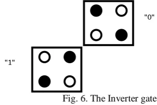
3.1 Inverter gate
Is created by putting together the two cells in an inverted manner. In this layout, whatever the layout of the first cell polarity (input), it will appear at the output of the inverter. Fig. 6 shows an Inverter gate.
Fig. 6. The Inverter gate
The sample is consistent with a stronger polarization, which can be implemented according to Fig. 7. In the layout, through putting together two inverted gates, as shown below, is used.
Fig. 7. Inverter gate with more polarization
3.2 Majority Gate
The gate has a number of input and one output and output cell polarization is achieved through the polarization of the majority inputs. Fig. 8 shows the alignment of majority gates and the table shows accuracy according to which equation (1) is defined, Fig. 8 majority Gate. As can be seen B and C inputs has been +1 Polarization. The result is that cell polarity output is +1[2]-[5]-[6].
Output = AB + AC + BC (1)
Copyright © 2015 CTTS.IN, All right reserved Fig. 8. The Majority gate
4.
C
LOCK IN THEQCA
In the logic circuits that are implemented, the clock is of utmost importance so much so that by applying a pulse to a cell the behavior of the cell are determined. The QCA has four different clocks whose brief descriptions are as follows:
4.1 Switch
In this phase, QCA cells are initially normal polarity. After a while, cells get out of state of peace and its amount becomes equal to the amount of input applied by the user or previous cell.
4.2 Hold
The cells is kept in the active mode and the energy level is maintained high and this cell may play a role in the input to the next cell.
4.3 Release
in this phase, the amount of energy in Cells slowly decreases so that it enters the relaxation phase. At this stage, the cell has no effect on its adjacent cells. There are no energy boundaries and no effect on neighboring cells.
4.4 Relax
In this phase, the cell's energy will be minimum and put in a state of peace. The cell has no effect on its adjacent cells.Fig. 9 shows four clocks in the QCA[7]-[8]-[9].
Fig. 9. Clocks in QCA
5.
I
NTRODUCTION TOS
EQUENTIALL
OGICC
IRCUITSThe basic concept of a sequential device is an important one that is fundamental in the design of digital systems. Recall that in combinational logic networks the output is a function of only the present input. In sharp contrast, the output of a sequential device depends not only on the present input but on previous inputs as well. This history of a sequential circuit's input is retained through the use of storage devices, that is, memory. It is the use of memory which adds a new dimension to logic design by providing the capability to solve numerous problems that cannot be handled by combinational logic alone. 5.1 Memory devices
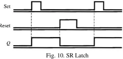
The two memory element types most commonly used in switching circuits are latches and flip-flops. A latch is a memory element whose excitation input signals control the state of the device: If a latch has an excitation input signal that forces the output of the device to 1, it is called a set latch. If it has an excitation input signal that forces the device output to 0, it is called a reset latch. If the device has both set and reset excitation signals, it is called a set-reset latch. Latch operation is illustrated in Fig. 10.
Fig. 10. SR Latch
Fig. 11. Excitation Table
Columns S and R are the inputs applied to an SR latch
while it is in state Q. The column labeled Q is the state of the SR latch before an input combination is applied to Sand R. The column labeled Q* is the state of the SR latch after the SR inputs have been applied and a steady-state result has been achieved. We call column Q the present state of the SR latch and column Q* the next state.
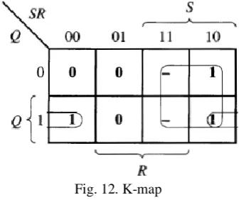
The information of Fig. 11 can be represented as a state diagram, as shown in Fig. 11, and plotted in K-map form, as shown in Fig. 12, where the value of the next state Q* is plotted as a function of the inputs, Sand R, and the present state Q. From this K-map can be derived the
following logic expression for Q*, called the
characteristic equation of the SR latch:
Fig. 12. K-map
Q* = S + R´Q (2)
The characteristic equation is so called because it characterizes the operation of the latch. For example, we can classify the operation of the latch into three cases:
Case 1: S = R = o. Equation (2) reduces to Q* = Q,
which indicates that the state does not change.
Case 2: S = I, R = o. Equation (2) reduces to Q* = 1,
representing the set operation.
Case 3: S = 0, R = 1. Equation (2) reduces to Q* = 0,
representing the reset operation[10].
6.
D
ESIGNING ANA
SYNCHRONOUSM
EMORYIn the previous section, the sequential circuits and very important application of a latch as a memory was
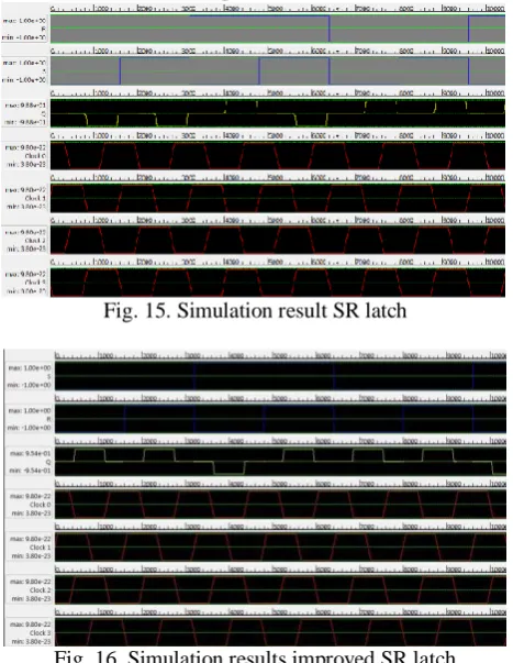
extensively discussed. We have seen that the difference between latch and flip-flop is in the clock signal and the latch is regarded as an asynchronous memory (sequential circuit). The scheme presented in Figure 13 an SR latch is implemented with the help of basic gates and in a single-layer manner. Set and Reset inputs, according to the three aforementioned states, sets and resets the circuit respectively and the result of simulation output clearly confirms the output characteristic equation. However, this circuit can be implemented as in Fig.14. In this method, the number of cells of 54 to 32 cells is decreased. Which establishes a 40% decrease in the total area of the circuit. In the second scheme through designing shorter strings and assigning the most appropriate design of the clock pulse, circuit speed is accelerated.
Fig. 13. SR latch is implemented in QCA Designer
Fig. 14. Improved implementation of SR latch
Copyright © 2015 CTTS.IN, All right reserved by the rising edge and it remains active until Reset. Upon
stimulation Reset the output is zero.
Fig. 15. Simulation result SR latch
Fig. 16. Simulation results improved SR latch
7. C
ONCLUSIONS ANDS
UGGESTIONS FORF
UTUREW
ORKCombinatorial and sequential logic circuits have a significant role in digital electronics. Memories are widely utilized in industry and the designs with lower power consumption are advancing towards microelectronics and nano-electronics at an ever increasing speed. Nano-electronics design platform for electronic devices are based on nano-meter size Scheme presented in this paper which is part of an unending expanse of quantum dot cellular automata and logic designs in nanometer. By means of minimizing the number of gates per unit area and the design briefly, the second inverter gate was a much smaller circuit. It also occupies less area.
Many other digital electronic devices are implementable in the logic which together can realize the dream of modern concepts such as quantum computing and finally quantum computing.
Then, in order to achieve a more complete sequential circuits as a memory logic, the proposed scheme can be used as the basic circuit and by dedicating pulse memory clock can become synchronous and by means of it, all JK, D, and T flip-flops can be more efficiently implement ed. Also, basic gates can be designed as programmable and the sum of these structures (and other necessities)
can be utilized as the basic blocks and the basis for designing a nano microprocessor.
R
EFERENCE[1] H. Jagarlamudi, M. Saha, P. Jagarlamudi, “Quantum Dot Cellular Automata Based Effective Design of Combinational and Sequential Logical Structures”,World Academy of Science, Engineering and Technology, Vol.5, 2011,12-25. [2] S. Karthigal Lakshmi, G. Athisha, “Effecient
Design of Logical Structures and Functions using Nanotechnology Based Quantum Dot Cellular Automata Design”,International Journal of Computer Applications (0975 8887), vol.3, no.5, June 2010.
[3] R. Zhou, X. Xia, F. Wang, Y. Shi, H. Liao, “A Logic Circuit Design of 2-4 Decoder Using Quantum Cellular Automata”,Journal of Computational Information Systems, 2012, 3463– 3469.
[4] N. Shah, F. Khanday, Z. Bangi, “Quantum Cellular Automata Based Efficient BCD Adder Structure”, CISME Vol.2, No.2 2012, 11-14. [5] F. Ahmad, G. Bhat, “Novel Code Converters
Based On Quantum-dot Cellular Automata (QCA)”, International Journal of Science and Research (IJSR), 2012, 358.
[6] S. Anuradha, B. Ravi, V. Pasar, “Design of five input majority gate Full Comparator using Quantum-Dot Cellular Automata”, nternational Journal of Ethics in Engineering & Management Education, Vol.1, April 2014.
[7] K. Walus, G.A. Jullien, V. Dimitrov, “Computer arithmetic structures for quantum cellular automata”, Asilomar Conference on Signals, Systems, and Computers, November 2003. [8] W. Wang, K. Walus, G.A. Jullien, “Quantum-dot
cellular automata adders”, IEEE Nano Conference, August 2003.
[9] R. Zhang, K. Walus, W. Wang, G. A. Jullien, “A method of majority logic reduction for quantum cellular automata”, IEEE Trans.Nanotechnol., vol.3, no.4, pp.443-450, Dec.2004.
[10] P. Nelson, H.Troy Nagle, J.David Irwin, D. Carroll, “Digital Logic Circuit Analysis & Design”, Prentice Hall, 1995.
A
UTHOR’
SP
ROFILEMohammad Reza Rasaei Moghaddam
2009. I hold master degree in Electronics from Islamic Azad University, science and research, Khorasan-e- Razavi Branch. I work on Industrial Automation and Calibrators projects.
My research interests include Nano Electronics design, Photovoltaic Systems and Solar Cells.
Ali Akbar Khazaei
Was born in Mashhad, Iran on May 09, 1969. He received his B.S. degree in Electronics engineering from Ferdowsi University of Mashhad in 1992, his M.Sc. and Ph.D degrees in Communication engineering from Tarbiat Modares University, Tehtan, Iran, in 1996 and Islamic Azad University, Science and Research Branch, Tehran, Iran in 2012 respectively.
He has been with the Electrical Engineering Department of Islamic Azad University, Mashhd Branch, Mashhd, Iran, from 2008, where he is an associate professor now. From 2000 to 2008, he was with the Satellite Communication group, Iran Telecommunication Research Center (ITRC), Tehran, Iran.
Davoud Bahrepour
was born in Mashhad, in 1982. He received the B.S. degree in Computer Engineering from the Sajjad Institute of Higher Education, Mashhad, Iran in 2005 and his M.S. and Ph.D. degrees in Computer Architecture from Science and Research Branch, Islamic Azad University, Tehran, Iran in 2007 and 2012 respectively.