Ames Laboratory Publications
Ames Laboratory
4-29-2009
Quasiperiodic layers of free-electron metals studied
using electron diffraction
A. K. Shukla
UGC-DAE Consortium for Scientific Research
R. S. Dhaka
UGC-DAE Consortium for Scientific Research
S. W. D'Souza
UGC-DAE Consortium for Scientific Research
Sanjay Singh
UGC-DAE Consortium for Scientific Research
D. Wu
Iowa State University
See next page for additional authors
Follow this and additional works at:
http://lib.dr.iastate.edu/ameslab_pubs
Part of the
Metallurgy Commons
The complete bibliographic information for this item can be found at
http://lib.dr.iastate.edu/
ameslab_pubs/62
. For information on how to cite this item, please visit
http://lib.dr.iastate.edu/
howtocite.html
.
Quasiperiodic layers of free-electron metals studied using electron
diffraction
Abstract
Using electron diffraction, we show that free-electron metals, such as sodium and potassium, form a highly
regular quasiperiodic monolayer on the fivefold surface of icosahedral Al-Pd-Mn and that the quasiperiodicity
propagates up to the second layer in sodium. Our photoelectron spectroscopy results show that the
quasicrystalline alkali-metal adlayer does not exhibit a pseudogap near the Fermi level thought to be
characteristic for the electronic structure of quasicrystalline materials. Calculations based on density
functional theory provide a model structure for the quasicrystalline alkali-metal monolayer and confirm the
absence of a pseudogap.
Disciplines
Metallurgy
Comments
This article is from
Physical Review B
79 (2009): 134206, doi:10.1103/PhysRevB.79.134206.
Authors
A. K. Shukla, R. S. Dhaka, S. W. D'Souza, Sanjay Singh, D. Wu, Thomas A. Lograsso, M. Krajčí, J. Hafner, K.
Horn, and S. R. Barman
Quasiperiodic layers of free-electron metals studied using electron diffraction
A. K. Shukla,1R. S. Dhaka,1S. W. D’Souza,1Sanjay Singh,1D. Wu,2T. A. Lograsso,2M. Krajčí,3,4J. Hafner,4
K. Horn,5 and S. R. Barman1
1UGC-DAE Consortium for Scientific Research, Khandwa Road, Indore 452001, India 2Ames Laboratory U.S. DOE, Iowa State University, Ames, Iowa 50011-3020, USA 3Institute of Physics, Slovak Academy of Sciences, SK-84511 Bratislava, Slovak Republic
4Center for Computational Materials Science, Universität Wien, A-1090 Wien, Austria 5Fritz-Haber-Institut der Max-Planck-Gesellschaft, D-14195 Berlin, Germany
共Received 19 November 2008; revised manuscript received 9 March 2009; published 29 April 2009兲 Using electron diffraction, we show that free-electron metals, such as sodium and potassium, form a highly regular quasiperiodic monolayer on the fivefold surface of icosahedral Al-Pd-Mn and that the quasiperiodicity propagates up to the second layer in sodium. Our photoelectron spectroscopy results show that the quasicrys-talline alkali-metal adlayer does not exhibit a pseudogap near the Fermi level thought to be characteristic for the electronic structure of quasicrystalline materials. Calculations based on density functional theory provide a model structure for the quasicrystalline alkali-metal monolayer and confirm the absence of a pseudogap.
DOI:10.1103/PhysRevB.79.134206 PACS number共s兲: 79.60.Dp, 73.20.At, 61.05.jh, 71.23.Ft
I. INTRODUCTION
Quasicrystals are complex alloys of metallic elements ex-hibiting anomalous properties such as high electrical resistiv-ity, low thermal conductivresistiv-ity, low frictional coefficient, and low surface energy.1In recent years, high-quality
quasicrys-talline surfaces have been prepared and their electronic struc-ture and morphology have been studied in detail.2–6This has
stimulated interest in the formation of quasiperiodic metallic films, using the quasicrystalline surface as template. Quasip-eriodic films consisting of a single element have been achieved only for a few cases共Sb, Bi, Cu, and Sn兲so far.7–9 To date, there is no clear understanding for which elements the interaction with the substrate might be sufficient to sta-bilize quasiperiodic order in the adlayer. Alkali metals such as sodium or potassium are the best examples of nearly-free-electron metals and it is an intriguing question whether the growth of pseudomorphic films of these metals might be used to produce a two-dimensional 共2D兲quasiperiodic free-electron metal.
Adsorption of alkali metals on metal surfaces has been a topic of active research because of interesting effects such as the decrease in the work function, existence of collective multipole excitations, and of quantum well states without a confining barrier.10,11Alkali-metal adsorption on the
alumi-num surface has been studied most extensively.10 The
five-fold surface of icosahedral共i兲Al-Pd-Mn has a similarity with the close-packed Al共111兲 surface, since it consists of a top-most dense Al-rich layer separated by a distance of only 0.48 Å by a layer with approximately 50% Al and 50% Pd, and the atomic density of these two layers together 共0.136 atoms/Å2兲 is similar to that of Al共111兲.2 Our x-ray
photoelectron spectroscopy study of Na and K films on i-Al-Pd-Mn showed that alkali-metal adlayers grow as a dis-persed phase 共i.e., not as condensed islands兲up to 1 mono-layer 共ML兲.12 Motivated by this work, the alkali-metal
growth on i-Al-Pd-Mn has been studied theoretically using ab initiodensity-functional methods and it was predicted that Na and K monolayers exhibit quasiperiodic order.13
An interesting feature of the electronic structure of many icosahedral quasicrystals is the formation of a “pseudogap,” i.e., of a minimum in the electronic density of states 共DOS兲 close to the Fermi level共EF兲. Many of the outstanding
prop-erties, such as their anomalous transport propprop-erties, have been attributed to the existence of the pseudogap.14 Photo-electron spectra show a rounding of the Fermi edge, which has been interpreted as the signature of such a DOS minimum.14–17 It is an interesting question whether the
strong coupling between adatoms and substrate necessary to impose quasiperiodic order also leads to the formation of a pseudogap in the DOS of the 2D adlayer. In this work, we show that Na and K quasiperiodic films can be prepared on the fivefold surface ofi-Al-Pd-Mn and report on the charac-terization of their geometric and electronic structures using low-energy electron diffraction 共LEED兲 and photoemission spectroscopy 共PES兲. We find good agreement between the experimental results and the theoretical predictions.13
II. EXPERIMENTAL
Single graini-Al-Pd-Mn quasicrystal with bulk composi-tion Al69.4Pd20.8Mn9.8 was grown using the Bridgman
tech-nique. The polished i-Al-Pd-Mn surface was cleaned by re-peated cycles of Ar+ sputtering 共1.5 keV, 45–60 min兲 and
annealing 共2–2.5 h兲 up to 870–900 K to produce large flat atomic surface. LEED and PES experiments have been per-formed using four-grid rear view ErLEED optics, and a Phoi-bos 100 electron energy analyzer, respectively. The base pressure of the experimental chamber was 6⫻10−11 mbar.
He I radiation 共h= 21.2 eV兲 was used for the photoemis-sion experiments. The resolution of the PES is about 0.1 eV at the measurement temperature共130 K兲. The composition of the quasicrystalline surface is Al74Pd21Mn5, as calculated
from area under the core-level peaks共Al 2p, Pd 3d, Mn 2p兲, i.e., very close to the bulk composition. Na and K were de-posited from well-degassed commercial Società Apparecchi Elettrici e Scientifici共SAES兲getter sources. The substrate is held at 130 K to avoid possible surface alloying that is ob-PHYSICAL REVIEW B79, 134206共2009兲
served for alkali metals at room temperature.18During
depo-sition, the chamber pressure rose to 9⫻10−11 mbar. The
thickness of the adlayers has been calculated from the area under the共Na 1sand K 2p兲and共Al 2p兲core-level peaks, as in our previous work.12,19The atomic density of a completed
monolayer is 0.067 atoms/Å2, corresponding to a coverage
of ⌰= 0.50, i.e., roughly equal to the coverage of the 共4
⫻4兲phase of Na on Al共111兲.10
III. RESULTS AND DISCUSSION
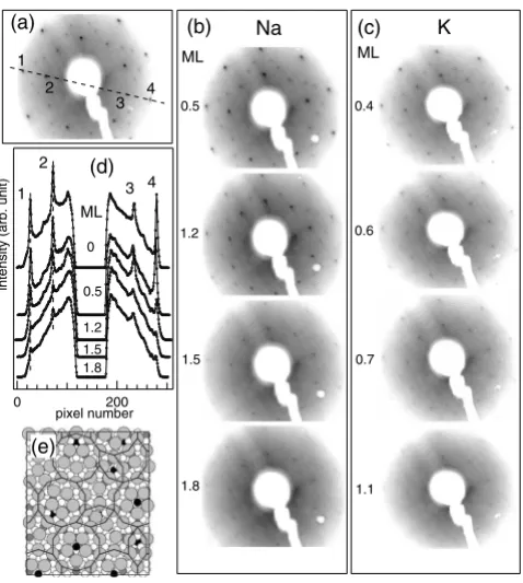
The structure of the alkali-metal overlayer oni-Al-Pd-Mn as seen in LEED recorded with 78 eV electron energy is shown in Fig.1. At such energies, LEED is sensitive prima-rily to the topmost layers due to the small mean-free path of the electrons.20In the LEED pattern of the cleani-Al-Pd-Mn
surface关Fig.1共a兲兴, an inner ring consisting of ten sharp spots is visible. A closer inspection of the spot intensities reveals two inequivalent sets of five spots, which agrees with the expected fivefold symmetry. An outer ring with similar ar-rangement of the inner ring is also visible. The LEED pattern
is in agreement with previous work on the fivefold i-Al-Pd-Mn surface.2,7
The fivefold symmetric LEED pattern persists upon dos-ing with Na or K, as shown in Figs. 1共b兲 and 1共c兲. The positions and widths of the LEED spots or the background remain mostly unchanged up to 1.2 ML Na coverage 关Fig. 1共b兲兴. This clearly shows that the Na adlayer grows pseudo-morphically and adopts the quasicrystalline symmetry of the substrate. For 1.5 ML of Na, the spot intensities slightly de-crease and the background intensity inde-creases. For 1.8 ML of Na, the spot intensities decrease further, with a concomitant increase in background, and the LEED spots intermediate between the inner and outer rings are hardly visible. This indicates that the quasiperiodic order in the Na adlayer de-creases above 1.2 ML. However, a distinctive fivefold LEED pattern exists up to 1.8 ML Na with no change in LEED spot positions. This suggests that the pseudomorphic growth con-tinues even for higher Na coverages共⬎1.2 ML兲. The results for K layers are slightly different as shown in Fig.1共c兲. The LEED spots for different coverages of K larger than 0.6 ML decrease in intensity and the intermediate spots disappear. However, a fivefold LEED pattern is visible up to 1.1 ML. Thus, K/i-Al-Pd-Mn films grow as a well-ordered quasicrys-talline film up to about 0.6 ML, while for higher coverages the degree of quasicrystalline order diminishes.
The intensity profiles of the diffraction spots are often used to obtain information about the degree of surface order.21 Splitting or significant broadening of the LEED
spots indicates the presence of surface defects, especially steps of different heights.22 Figure 1共d兲 shows the intensity
profile of the LEED spots as a function of Na coverage along a dashed line joining two of the most intense spots: 1 and 4 in Fig. 1共a兲. The peaks in intensity profile correspond to the observed LEED spots, which are numbered in Fig.1共a兲. Flat portions in the profiles are due to the shadow of the electron gun.
Important observations can be made from the intensity profiles. First, with increasing coverage of Na, there is no change in the LEED spot positions. The ratio of the distances between the LEED spots forming the inner and outer rings from the center 共specular spot兲remains equal to the golden mean⬇1.61兲. Second, a splitting of the LEED spots is not observed indicating that the adlayer is atomically smooth. Finally, we do not observe the emergence of any extra spots after Na adsorption up to the highest coverage. Similar in-tensity profiles are obtained for K adlayers.
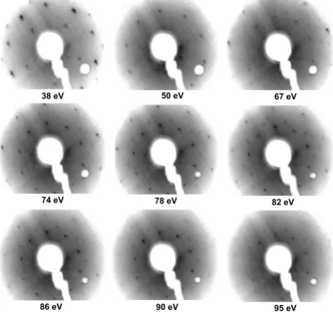
It is well known that the presence of step arrays on the surface results in the splitting of LEED spots.23–25Occurence
of the periodically alternating single and splitted integer or-der spots with increasing electron-beam energies 共i.e., in-creasing radius of Ewald’s sphere兲has been attributed to an out-of-phase scattering of subsequent terraces and a formula was derived to determine the characteristic electron energies for sharp LEED spots.24,25Figure2shows the LEED patterns
of 1.2 ML Na recorded at various electron-beam energies. LEED spots of fivefold diffraction pattern continuously con-verge toward the specular spot共hidden by the shadow of the electron gun兲with increasing incident beam energies and we do not observe the splitting of the LEED spots at any elec-tron energy. It clearly excludes the presence of step defects in the adlayer. intensity (arb. unit) 200 0 pixel number 0 0.5 1.2 1.5 1.8 ML 1 2 3 4
(a) (b) (c)
[image:4.609.55.294.65.331.2](d) Na K ML ML 1 2 0.5 1.2 1.5 1.8 0.7 0.6 0.4 3 4 1.1 (e)
FIG. 1. 共a兲 LEED pattern of a cleani-Al-Pd-Mn surface. Dif-fraction spots are numbered to facilitate their identification in the intensity profiles关shown in共d兲兴along the dashed line going through different spots.共b兲and共c兲show LEED patterns measured at 130 K for different Na and K coverages oni-Al-Pd-Mn, respectively. Im-ages are shown in inverted gray scale where black indicates the highest brightness. All the LEED patterns have been recorded at 78 eV electron-beam energy.共d兲Intensity profile as a function Na cov-erage along the dashed line is shown in共a兲.共e兲The atomic structure of an adsorbed K monolayer on the Al-Pd-Mn substrate where Al: small open circles, Pd: small gray circles, Mn: small black circles, and K: large gray circles. The quasiperiodic ordering is represented by the DHBS tiling共cf. text兲.
SHUKLAet al. PHYSICAL REVIEW B79, 134206共2009兲
If an adlayer has different domains or twinned structures with a specific orientational relationship with the substrate then it results in the appearance of multiple spots in the LEED pattern. There are reports of rotational epitaxy for different metals 共Al, Ag, Fe, and Ni兲grown oni-Al-Pd-Mn, where the adlayer forms as five crystalline domains reflecting the substrate symmetry and the formation of such domains results in the extra spots in the LEED pattern of metal films on the quasicrystalline surfaces.6,26 The LEED patterns for
1.2 ML Na recorded at various electron energies共Fig.2兲do not show the presence of such multiple spots. We also do not observe the multiple spots in LEED pattern of K adlayers. This eliminates the possibility of the formation of twinned nanocrystallites or crystalline domains in the alkali-metal ad-layers.
The geometric structure of a fivefold surface of i-Al-Pd-Mn is well described by a P1 tiling consisting of pentagons, pentagonal stars, boats, and thick and thin golden rhombi,5,13,27as confirmed also by atomically resolved
scan-ning tunneling microscopy.28 The surface consists of two
closely spaced atomic layers with a vertical separation of only 0.48 Å. The top layer is occupied by a majority of Al atoms and ⬇4 at.% of Mn, while the second layer is com-posed in a ratio of about 1:1 by Pd and Al atoms with a small concentration of Mn atoms. Half of the vertices of the P1 tiling is decorated by these Pd atoms, while most of the remaining vertices correspond to Pd atoms in deeper layers. In the surface plane, these sites are surrounded by complete or incomplete pentagons of Al atoms.
Our mapping of the potential-energy surface of an alkali atom on the i-Al-Pd-Mn surfaces using ab initio density functional theory 共DFT兲 techniques 关we used the VASP code29兴demonstrates that the vertices of the P1 tiling共
deco-rated by Pd atoms located 0.48 Å below the surface and
characterized by minima in the surface electron density兲are indeed the energetically most favorable adsorption sites. Hence, these sites were chosen to form the skeleton of the adlayer structure, the interior of the tiles being decorated in a way compatible with the overall fivefold symmetry, and an atomic density of 0.66 atoms/Å2共corresponding to⌰= 0.5兲. Relaxation of the starting structure under the action of theab initiocalculated forces resulted in a spontaneous rearrange-ment of the adatoms in a highly regular quasiperiodic struc-ture different from the initial strucstruc-ture, with atomic positions conforming with a decagon-hexagon-boat-star 共DHBS兲 til-ing. The alkali atoms initially placed onto the vertices of the P1 tiling remain in their positions, but the atoms decorating the interior of the tiles move in such a way as to form an even more regular structure—the relaxed equilibrium struc-ture in a K adlayer is shown in Fig. 1共e兲. The shortest ideal distance between atoms forming the pentagonal motifs in the relaxed adlayer is 3.60 Å, only in the boat tile a few dis-tances of 3.41 Å are observed. Hence, this structure is ide-ally suited for a regular adlayer of Na atoms 共atomic diam-eter 3.7 Å as calculated for bulk Na兲, while a K adlayer 共atomic diameter 4.6 Å兲is already slightly over packed, as reflected by a somewhat larger corrugation of the adlayer. Thicker films may be formed by depositing a second layer of adatoms into hollow sites of the first monolayer. A stable quasiperiodic bilayer structure is formed if the coverage in the second layer is reduced to ⌰= 0.39, while quasiperiodic order decreases rapidly by addition of further atomic layers. The theoretical predictions based on density functional theory are consistent with our experimental observation of quasiperiodic ordering in a Na overlayer atT= 130 K, which gradually disappears above 1.8 ML. The calculations show that both K and Na monolayers exhibit the same quasiperi-odic pattern; however, the lateral ordering in a K monolayer is less regular and the monolayer is more corrugated. In the experiment, it is seen that the quasiperiodicity of a K film is affected even below monolayer thickness, which is not the case for Na. The different degree of ordering in Na and K layers arises from the different atomic size. In the idealized DHBS structure the distances between the K atoms are al-ready somewhat compressed, leading to a stronger corruga-tion and a less perfect quasiperiodic order and these effects become even more pronounced with increasing coverage.
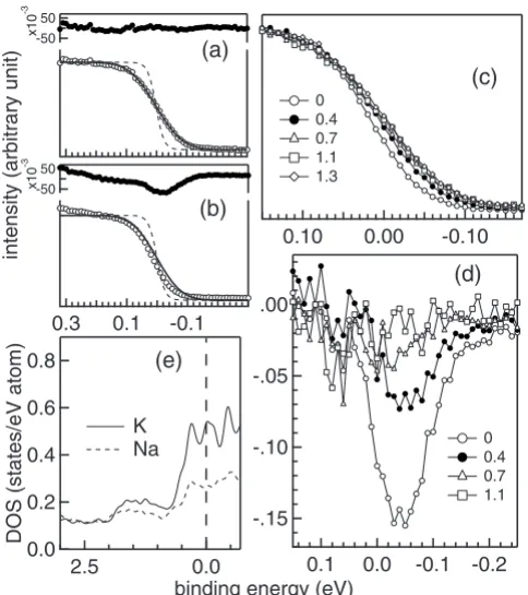
Having demonstrated the formation of a 2D quasiperiodic system consisting of a single free-electron metal, we are in a position to compare its electronic structure to that of ordinary three-dimensional bulk quasicrystals. Here, the central ques-tion is whether the pseudogap structure of the electronic DOS of the substrate is also imprinted upon the 2D adlayer. To resolve this question, we have performed electronic struc-ture calculations and PES experiments covering the region aroundEF 共Fig.3兲. If a pseudogap at the Fermi level exists,
the photoemission spectrum nearEFcannot be modeled
sim-ply by a Fermi function;14–17rather the measured intensities
show a slow decrease in approachingEF. By comparing the
spectral function nearEF for cleani-Al-Pd-Mn and
progres-sively higher coverages of K, we show that the signature of a pseudogap clearly found ini-Al-Pd-Mn is absent in the qua-sicrystalline K layer. We analyze the spectra for a 1.3 ML K film and a cleani-Al-Pd-Mn surface by fitting with a Fermi
38 eV 50 eV 67 eV
74 eV 78 eV 82 eV
[image:5.609.54.291.70.292.2]86 eV 90 eV 95 eV
FIG. 2. LEED patterns of 1.2 ML Na grown on i-Al-Pd-Mn surface at several incident electron-beam energies. Images are shown in inverted gray scale where black indicates the highest brightness. All the LEED patterns have been recorded at 130 K.
QUASIPERIODIC LAYERS OF FREE-ELECTRON METALS… PHYSICAL REVIEW B79, 134206共2009兲
function convoluted with the instrumental Gaussian broaden-ing关Figs.3共a兲and3共b兲兴. Least-square error minimization is performed by freely varying the position, intensity of the Fermi function, and the full width at half maximum of the Gaussian. The residual at the top of Fig.3共a兲shows the good quality of the fit for 1.3 ML of K, indicating that no DOS minimum at the Fermi level exists for the K adlayer. On the other hand, because of a pseudogap the residual exhibits a dip in clean i-Al-Pd-Mn关Fig.3共b兲兴. This dip, which is the signature of the pseudogap, appears slightly above EF, in
agreement with earlier literature.17,30
The absence of a pseudogap in alkali-metal adlayers on i-Al-Pd-Mn is clearly observed from the coverage-dependent spectra 关Fig. 3共c兲兴. The spectral intensity slightly aboveEF
gradually increases with increasing coverage of K. The dif-ference spectra in Fig. 3共d兲 obtained by subtracting the 1.3 ML K/i-Al-Pd-Mn spectrum from those with lower K cov-erage unambiguously show the progressive filling up of the pseudogap with increasing K coverage. Note that at a cover-age of 0.7 ML K, where the LEED data in Fig. 1共c兲 show that the layer is clearly quasiperiodic, the PES shows that no pseudogap exists. These experimental observations are in good agreement with DFT predictions. Figure3共e兲shows the calculated DOS for Na and K monolayers on i-Al-Pd-Mn
around EF. For a Na monolayer, we find a continously
in-creasing DOS, while for a K monolayer, we even find a strongly increasing DOS at binding energies below 0.5 eV. This is the result of compressed K-K distances leading to an incipient occupation of K 3d states 共as also in compressed bulk K兲.
This is an interesting finding because the existence of a pseudogap nearEF is sometimes considered as an important
factor contributing to the stability of the quasicrystalline phases共although it is evident that pseudogaps exist not only in quasicrystals but also in many crystalline alloys such as Al-Mn and even amorphous alloys31,32兲. In any case, the
ex-istence of a deep pseudogap is an indication of a consider-able degree of covalency in the interaction between the Al and the transition-metal atoms.33 Previous investigations
共both theoretical30 and experimental34兲 of the surface
elec-tronic structure of i-Al-Pd-Mn have demonstrated that the metallic character of the bonding is enhanced at the surface and that the pseudogap is partially leveled out as a conse-quence of a strong relaxation of the near-surface Al atoms. The present work extends these studies to the electronic structure of a well-ordered quasiperiodic adlayer and we find that the pseudogap has disappeared. This has important con-sequences on the mechanism stabilizing the quasiperiodic structure of the films quasiperiodicity is imprinted on the first monolayer by the strong binding of the adatoms in surface charge-density minima. Atoms in the second monolayer are also adsorbed in hollow sites of the first layer, but because the binding between the alkali atoms is much weaker than with the substrate, the quasiperiodic order is gradually lost in multilayers.
IV. CONCLUSION
We have performed low-energy electron diffraction, ultra-violet photoemission, andab initiodensity functional theory calculations to show that free-electron metals, such as so-dium and potassium, form a highly regular quasicrystalline monolayer on i-Al-Pd-Mn. In the case of Na, the quasiperi-odicity propagates up to the second layer. The existence of quasicrystalline alkali-metal adlayers and that it propagates to the second layer in Na are in good agreement with the previously published density functional theory results. Pho-toelectron spectroscopy results show that the pseudogap of thei-Al-Pd-Mn substrate is gradually filled up as alkali metal is deposited. Quasicrystalline alkali-metal adlayer does not exhibit a pseudogap near the Fermi level thought to be char-acteristic for the electronic structure of quasicrystalline ma-terials. The DOS of an quasicrystalline alkali-metal mono-layer oni-Al-Pd-Mn calculated by density functional theory also shows the absence of a pseudogap.
ACKNOWLEDGMENTS
Funding from Max Planck Institute, Germany, Depart-ment of Science and Technology, India, Ramanna Research Grant, and U.S. Department of Energy Basic Energy Sci-ences is gratefully acknowledged.
-.15 -.10 -.05 .00 -0.2 -0.1 0.0 0.1 0 0.4 0.7 1.1 (d) -0.10 0.00 0.10 0 0.4 0.7 1.1 1.3 (c)
binding energy (eV)
[image:6.609.52.294.66.338.2]intensity (arbitrary unit ) 50 -50 x10 -3 (a) 50 -50 x10 -3 -0.1 0.1 0.3 (b) 0.8 0.6 0.4 0.2 0.0 DOS (states/eV atom) 2.5 0.0 K Na (e)
FIG. 3. Photoemission spectra in the near EF region 共open circles兲 of 共a兲 1.3 ML K coverage on i-Al-Pd-Mn and 共b兲 clean i-Al-Pd-Mn surface at 130 K共open circles兲. The fitted curve共thick solid line兲 and Fermi function 共dashed line兲 are also shown. Re-sidual of fitting is shown at the top of each spectra.共c兲Closeup of near Fermi edge region as a function of K coverage. Spectra are normalized to the same height at 0.1 eV.共d兲The difference spectra are obtained by subtracting the nearEFregion spectrum of 1.3 ML K from those of other K coverages shown in共c兲.共e兲The calculated DOS of Na and K monolayer adsorbed oni-Al-Pd-Mn.
SHUKLAet al. PHYSICAL REVIEW B79, 134206共2009兲
1D. Shechtman, I. Blech, D. Gratias, and J. W. Cahn, Phys. Rev.
Lett. 53, 1951共1984兲.
2M. Gierer, M. A. Van Hove, A. I. Goldman, Z. Shen, S.-L.
Chang, C. J. Jenks, C.-M. Zhang, and P. A. Thiel, Phys. Rev. Lett. 78, 467共1997兲.
3Eli Rotenberg, W. Theis K. Horn, and P. Gille, Nature共London兲
406, 602共2000兲.
4J. C. Zheng, C. H. A. Huan, A. T. S. Wee, M. A. Van Hove, C. S.
Fadley, F. J. Shi, E. Rotenberg, S. R. Barman, J. J. Paggel, K. Horn, P. Ebert, and K. Urban, Phys. Rev. B 69, 134107共2004兲. 5M. Krajčí and J. Hafner, Phys. Rev. B 71, 184207共2005兲. 6H. R. Sharma, M. Shimoda, and A. P. Tsai, Adv. Phys. 56, 403
共2007兲.
7K. J. Franke, H. R. Sharma, W. Theis, P. Gille, Ph. Ebert, and K.
H. Rieder, Phys. Rev. Lett. 89, 156104共2002兲.
8J. Ledieu, J. T. Hoeft, D. E. Reid, J. A. Smerdon, R. D. Diehl, T.
A. Lograsso, A. R. Ross, and R. McGrath, Phys. Rev. Lett. 92, 135507共2004兲.
9H. R. Sharma, M. Shimoda, A. R. Ross, T. A. Lograsso, and A.
P. Tsai, Phys. Rev. B 72, 045428共2005兲.
10Physics and Chemistry of Alkali Metal Adsorption, edited by H. P. Bonzel, A. M. Bradshaw, and G. Ertl共Elsevier, Amsterdam, 1989兲.
11S. R. Barman, P. Haberle, K. Horn, J. A. Maytorena, and A.
Liebsch, Phys. Rev. Lett. 86, 5108共2001兲.
12A. K. Shukla, R. S. Dhaka, C. Biswas, S. Banik, S. R. Barman,
K. Horn, Ph. Ebert, and K. Urban, Phys. Rev. B 73, 054432
共2006兲.
13M. Krajčí and J. Hafner, Phys. Rev. B 75, 224205共2007兲. 14Physical Properties of Quasicrystals, edited by Z. M. Stadnik,
Springer Series in Solid-State Sciences Vol. 126共Springer, Ber-lin, 1999兲.
15X. Wu, S. W. Kycia, C. G. Olson, P. J. Benning, A. I. Goldman,
and D. W. Lynch, Phys. Rev. Lett. 75, 4540共1995兲.
16Z. M. Stadnik, D. Purdie, M. Garnier, Y. Baer, A.-P. Tsai, A.
Inoue, K. Edagawa, and S. Takeuchi, Phys. Rev. Lett. 77, 1777
共1996兲.
17G. Neuhold, S. R. Barman, K. Horn, W. Theis, P. Ebert, and K.
Urban, Phys. Rev. B 58, 734共1998兲.
18S. R. Barman, C. Stampfl, P. Haberle, W. Ibanez, Y. Q. Cai, and
K. Horn, Phys. Rev. B 64, 195410共2001兲.
19A. K. Shukla, S. Banik, R. S. Dhaka, C. Biswas, S. R. Barman,
and H. Haak, Rev. Sci. Instrum. 75, 4467共2004兲.
20S. Tanuma, C. J. Powell, and D. R. Penn, Surf. Interface Anal.
17, 911共1991兲.
21K. D. Gronwald and M. Henzler, Surf. Sci. 117, 180共1982兲. 22Surface Crystallography by LEED, edited by M. A. Van Hove
and S. Y. Tong, Series in Chemical Physics Vol. 2共Springer, Berlin, 1979兲.
23W. P. Ellis and R. L. Schwoebel, Surf. Sci. 11, 82共1968兲. 24M. Henzler, Surf. Sci. 19, 159共1970兲; Appl. Phys.共Berlin兲 9,
11共1976兲.
25O. Janzen, Ch. Hahn, T. U. Kampen, and W. Monch, Eur. Phys.
J. B 7, 1共1999兲.
26B. Bolliger, V. E. Dmitrienko, M. Erbudak, R. Lüscher, H.-U.
Nissen, and A. R. Kortan, Phys. Rev. B 63, 052203共2001兲. 27Z. Papadopolos, G. Kasner, J. Ledieu, E. J. Cox, N. V.
Richard-son, Q. Chen, R. D. Diehl, T. A. Lograsso, A. R. Ross, and R. McGrath, Phys. Rev. B 66, 184207共2002兲.
28M. Krajčí, J. Hafner, J. Ledieu, and R. McGrath, Phys. Rev. B
73, 024202共2006兲.
29G. Kresse and D. Joubert, Phys. Rev. B 59, 1758共1999兲. 30M. Krajci and J. Hafner, Phys. Rev. B 71, 054202共2005兲. 31J. Hafner and M. Krajci, Phys. Rev. B 47, 11795共1993兲. 32A. K. Shukla, C. Biswas, R. S. Dhaka, S. C. Das, P. Krüger, and
S. R. Barman, Phys. Rev. B 77, 195103共2008兲.
33M. Krajčí and J. Hafner, Phys. Rev. B 68, 165202共2003兲. 34V. Fournée, P. J. Pinhero, J. W. Anderegg, T. A. Lograsso, A. R.
Ross, P. C. Canfield, I. R. Fisher, and P. A. Thiel, Phys. Rev. B
62, 14049共2000兲.
QUASIPERIODIC LAYERS OF FREE-ELECTRON METALS… PHYSICAL REVIEW B79, 134206共2009兲