Reduced Switch Single-Phase Five-Level Inverter for Grid
Connected PV System
Jisi Nalupurakkandiyil
1, T G Sanish Kumar
21
Asst. Professor, Thejus Engineering College, Thrissur,, Kerala, India
2
Asst. Professor, Government Engineering College, Thrissur, Kerala, India
1. Introduction
Because of the rapid population growth and industrialization, the demand for electricity is growing day by day, and we may not be able to meet our demands with our central power generation system. Also the diminishing deposits of non-renewable energy sources such as coal, natural gas, fossil fuels etc. leads to energy crisis. So new technologies should be developed to produce energy in a most environment-friendly manner and it should be utilized in a most efficient way. We have to find use of other sources like solar, wind, geothermal etc. for energy generation other than our conventional sources like hydro, thermal and nuclear. Out of these renewable sources, one of the main sources is solar energy.
Solar energy is a renewable, inexhaustible and ultimate source of energy and the photovoltaic technique which uses solar energy has its own advantages like the source is quite free, no fuel is required, produces no waste etc.However, PV system has gained less support from private sectors and users due to the high cost to install the system and long payback time from the system.
S1
PV Array
L1 D1
C
DC-DC Boost Converter
S2
S5
S4
S3
Lf
Grid
Full-Bridge Inverter
Vg
Ig
Fig.1 Conventional grid connected PV system
Abstract: A reduced switch multi-level inverter for grid connected photovoltaic (PV)system is presented in this paper. A conventional grid connected PV system uses full-bridge inverters which results a three level output. Inverter output THD can be reduced by increasing its number of levels. For that we can use conventional multi-level inverters like diode clamped, flying capacitor and cascaded-H bridge. But, in all these topologies, the number of circuit elements increases with increase in number of levels. The multi-level inverter discussed in this work offers higher power capability with lower harmonics and lower switching losses with an additional advantage of reduction in the number of power electronic switches using an auxiliary circuit arrangement. A conventional grid PV system and PV system with reduced switch five-level inverter are simulated using MATLAB/Simulink and the results are analyzed. Also, in simulation THD of the above two systems are compared.
A conventional single phase photovoltaic system which is shown in Fig.1 comprises a boost converter and an inverter .The output of PV array is stepped up using dc-dc converter (either boost or buck-boost can be used) and after inversion it is fed to grid/load.
Fig.2 Output voltage levels of a full bridge inverter with Vpv as input
In conventional system, we are using a full bridge inverter which results a three level output, ie +voltage, zero and –voltage levels. Ideal three-level output of an inverter is shown in Fig.2. If we need more sinusoidal output from the inverter or if we want to reduce the THD of inverter output, we can increase the number of levels of the inverter. For that we can use multi-level inverters. The conventional multi-level topologies are diode clamped, flying capacitor and cascaded-H bridge. But the main problem with these multi-level inverters are, if we increase the number of multi-levels, the number of switching devices and other circuit components have to be increased. Thus the system size increases, cost increases, circuit complexity increases and the control will become more difficult.
2. Grid Connected Pv System With Reduced Switch Five-Level Inverter
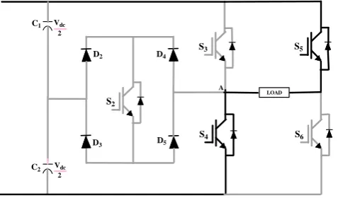
A single-phase grid connected PV system with reduced switch five-level inverter is shown in Fig.3 [6] and [7]. The inverter adopts a full-bridge configuration with an auxiliary circuit. PV arrays are connected to the inverter via a dc–dc boost converter to step up the output of PV module.By introducing an auxiliary circuit between dc-dc converter and full-bridge inverter, we can increase the number ofinverter output levels to five which is shown in Fig.4 [5].
MPPT
PI Controller PWM
From PV array
Vpv
Ipv
_ + Ppv
to switches S2-S5
Iref
Vg
Ig
Fig.3 Grid connected PV system with reduced switch Five-level inverter
The auxiliary circuit consists of one switch and four diodes. So here a total of five switches, ie one switch of this auxiliary circuit and four switches of full bridge inverters are enough to get a five-level output. But, all other conventional multi-level inverters require a minimum of eight power electronic switches to generate a five-level output. Thus the system cost reduces, size reduces and circuit complexity reduces.
A filtering inductance Lf is used to filter the current injected into the grid. The injected current must be
sinusoidal with low harmonic distortion. PI current control scheme is employed to keep the output current sinusoidal and to maintain the power factor at near unity. The irradiance level in inconsistent throughout the day, the amount of electric power generated by this solar module is changing with weather conditions. To overcome this problem or to track the maximum power from solar array, maximum power point tracking (MPPT) algorithm is used. The feedback PI current control senses the current injected into the grid, also known as grid current Ig and feedback to a comparator which compares it with the current Iref. Iref is obtained from the
grid voltage by multiplying it with the variable m. Variable m is derived from the MPPT algorithm. As the
irradiance level increases, m also increases and we can represent it as„m‟ α irradiance of the sun
The instantaneous current error from the comparison between Iref and Ig is fed to a PI controller. The
integral term of PI controller improves the tracking by reducing the instantaneous error between the reference and the actual current. The resulting error signal is compared with a triangular carrier signal and the control signals for full bridge inverter are generated based on this comparison. This is to ensure that grid current is in phase with grid voltage and always at near unity power factor.
a. Working Principle-(Dual Reference Modulation Technique)
Two reference signals Vref1 and Vref2 will take turns to be compared with the carrier signal at a time [6] and
[7]. If Vref1 exceeds the peak amplitude of the carrier signal Vcarrier, Vref2 will be compared with the carrier signal
until it reaches zero. At this point onward, Vref1 takes over the comparison process until it exceeds Vcarrier. This
will lead pattern, as shown in Fig.5. Switches S2–S4 will be switching at the rate of the carrier to a switching
signal frequency, whereas S5 and S6 will operate at a frequency equivalent to the fundamental frequency.
Fig.5 Switching pattern for the single phase five level inverter
b. Power Stage Operation
The required five voltage output levels (Vdc, Vdc/2, 0, -Vdc/2, -Vdc) are generated as follows:
S2
S3
S4
S5
S6
C1
C2
D2
D3
D4
D5
LOAD
Vdc 2
2 Vdc
A
1) Maximum positive output, Vdc: Switch S3 is ON, connecting the load positive terminal to A, and switch S6 is
ON, connecting the load negative terminal to ground. All other controlled switches are OFF. Fig.6 shows the current paths that are active at this stage.
S2 S3 S4 S5 S6 C1 C2 D2 D3 D4 D5 LOAD Vdc 2 2 Vdc A
Fig.7 Switching pattern required to generate output voltage level Vdc/2
2) Half-level positive output, Vdc/2: The auxiliary switch, S2 is ON, connecting the load positive terminal to
point A, through diodes D2 and D5, and switch S6 is ON, connecting the load negative terminal to ground. All
other controlled switches are OFF. Fig.7 shows the current paths that are active at this stage.
S2 S3 S4 S5 S6 C1 C2 D2 D3 D4 D5 LOAD Vdc 2 2 Vdc A
Fig.8 Switching pattern required to generate output voltage level zero.
3) Zero output: The two main switches S3 and S4 are ON, leads to short-circuit. All other controlled switches are
OFF. Fig.8 shows the current paths that are active at this stage.
S2 S3 S4 S5 S6 C1 C2 D2 D3 D4 D5 LOAD Vdc 2 2 Vdc A
4) Half-level negative output, -Vdc/2: The auxiliary switch, S2 is ON, connecting the load positive terminal to
point A, through diodes D3 and D4, and S5 is ON, connecting the load negative terminal to ground . All other
controlled switches are OFF. Fig.9 shows the current paths that are active at this stage.
S2 S3 S4 S5 S6 C1 C2 D2 D3 D4 D5 LOAD Vdc 2 2 Vdc A
Fig.10 Switching pattern required to generate output voltage level –Vdc
5) Maximum negative output, -Vdc: Switch S5 is ON, connecting the load negative terminal to A, and S4 is ON,
connecting the load positive terminal to ground. All other controlled switches are OFF. Fig.10 shows the current paths that are active at this stage.
Table I gives the switching combinations to generate the five-level output with reduced switch topology and Table II gives the comparison of different multi-level inverter topologies on the basis of number of circuit components to get a five-level output
Table I : Switching combinations to generate five level output
S2 S3 S4 S5 S6 Vout
ON OFF OFF OFF ON +Vdc/2
OFF ON OFF OFF ON +Vdc
OFF OFF or (ON) OFF or (ON) ON or (OFF) ON or (OFF) 0
ON OFF OFF ON OFF -Vdc/2
OFF OFF ON ON OFF -Vdc
Table II : Comparison of different multi-level inverter topologies
Converte r type: Diode clampe d Flying capacit or Cascad ed H-Bridge Reduce d switch Switching
devices 8 8 8 5
Main
diodes 8 8 8 8
Clamping
diodes 6 or 12 0 0 0
2.3 MPPT for PV system
The output of PV panel changes with the changes in climatic condition such as temperature and insolation level. In order to track maximum power from solar array, maximum power point trackers (MPPT) are used. P-V and I-V characteristic of a PV module with maximum power point (MPP) is shown in Fig.11.
VMPP VOC
IMPP
ISC
PMPP
PV Voltage (V)
P
V
C
u
rr
en
t
(A
)
P
V
P
o
w
er
(
W
)
Fig.11 P-V and I-V characteristics of a PV module
Many MPPT techniques have been developed for PV systems to track the maximum power point of the system; examples are the Perturb and Observe (P&O), Incremental Conductance (IC), MPPT based on FLC etc. The P&O algorithm is very popular and simple. This method finds the maximum power point of PV modules by means of iteratively perturbing, observing and comparing the power generated by the PV modules. It is widely applied to the maximum power point tracker of the photovoltaic system for its features of simplicity and convenience. The required parameters for P&O MPPT algorithms are only the voltage and current of PV module.
Fig.12 Power graph for P&O algorithm
Read V(k), I(k), and calculate P(k)=V(k)*I(k)
START
Delay P(k) & V(k) by (k-1) instant; P(k-1), V(k-1)
Increase D Decrease D Decrease D Increase D
To switch
0
P
0
V V0
) 1 ( ) (
) 1 ( ) (
k V k V V
k P k P P
Yes
Yes Yes
No
No No
Fig.13 Flow Chart of P&O MPPT Algorithm
3. Simulation Results
Fig.14 (a) and Fig.14 (b) gives the P-V and I-V characteristics of PV array at constant temperature and for varying irradiance respectively.
Irradiance:
I-1000W/m2 II-900W/m2
III-800W/m2 IV-500W/m2
Fig.14 (b) IV characteristic of PV array at constant temperature and for varying irradiance
The two reference signals and the carrier signal for dual reference modulation PWM technique are
shown in Fig.15 and the control signals to switches S2-S6 are shown in Fig.15 (a) to Fig.15 (e).
Fig.15 PWM signal generation (Dual reference modulation)
Fig.15 (a) PWM switching signal to S2
Fig.15 (b) PWM switching signal to S3
Fig.15 (d) PWM switching signal to S5
Fig.15 (e) PWM switching signal to S6
Fig.16 Grid voltage, inverter output voltage and inverter current of PV system with reduced switch topology
Fig.17 Grid voltage, inverter output voltage and inverter current of conventional PV system
Fig.18 (a) FFT analysis for PV system with new topology
Fig.18 (b) FFT analysis for Conventional PV system
From FFT analysis shown in Fig.18 (a) and Fig.18 (b)it is very clear that THD can be reduced with an auxiliary circuit arrangement between boost converter and full bridge inverter compared to conventional PV system.
4. Conclusions
References
[1]. N. S. Choi, J. G. Cho, and G. H. Cho, “A general circuit topology of multilevel inverter,” in Proc. IEEE 22th Annu. PESC, Jun. 24–27, 1991, pp. 96–103.
[2]. V. G. Agelidis, D. M. Baker, W. B. Lawrance, and C. V. Nayar, “A multilevel PWM inverter topology
for photovoltaic applications,” in Proc. IEEE ISIE, Guimarães, Portugal, 1997, pp. 589–594.
[3]. S. J. Park, F. S. Kang, M. H. Lee, C. U. Kim, “A New Single-Phase Five Level PWM Inverter
Employing a Deadbeat Control Scheme,” IEEE Trans. Power Electronics., vol. 18, no. 18, pp. 831-843, May. 2003.
[4]. S. B. Kjaer, J. K. Pedersen, and F. Blaabjerg, “A review of single-phase grid connected inverters for
photovoltaic modules,” IEEE Trans. Ind. Appl., vol. 41, no. 5, pp. 1292–1306, Sep./Oct. 2005. 6.
[5]. Gerardo Ceglia, VíctorGuzmán, Member, IEEE, Carlos Sánchez, Fernando Ibáñez, Julio Walter, and
María I. Giménez, Member, IEEE “A New Simplified Multilevel Inverter Topology for DC–AC Conversion”, IEEE Transactions on power electronics, vol. 21, no. 5, september 2006.
[6]. JeyrajSelvaraj and Nasrudin A. Rahim, “Multilevel Inverter For Grid-Connected PV System
Employing Digital PI Controller,” IEEE transactions on industrial electronics, vol. 56, no. 1, january 2009.
[7]. N. A. Rahim, Senior Member, IEEE, J. Selvaraj “Multilevel Inverter with Dual Reference Modulation
Technique for Grid-Connected PV System” IEEE Transactions on industrial electronics, vol. 57, no. 6, june 2010.
[8]. TrishanEsram, Patrick L. Chapman, Senior Member, IEEE, “Comparison of Photovoltaic Array
Maximum PowerPoint Tracking Techniques”, IEEE Transactions on energy conversion, vol. 22, no. 2, june 2007.
[9]. Muhammad H. Rashid, Power electronics: Circuits, Devices, and Applications, 3rd ed. Pearson