Theory of circuit block switch-off
S. Henzler1, J. Berthold2, G. Georgakos2, and D. Schmitt-Landsiedel1
1Lehrstuhl f¨ur Technische Elektronik, Technische Universit¨at M¨unchen, Theresienstrasse 90, D-80290 Munich, Germany 2Corporate Logic, Infineon Technologies AG, Balanstrasse 73, D-81541 Munich, Germany
Abstract. Switching-off unused circuit blocks is a promis-ing approach to supress static leakage currents in ultra deep sub-micron CMOS digital systems. Basic performance pa-rameters of Circuit Block Switch-Off (CBSO) schemes are defined and their dependence on basic circuit parameters is estimated. Therefore the design trade-off between strong leakage suppression in idle mode and adequate dynamic per-formance in active mode can be supported by simple analytic investigations. Additionally, a guideline for the estimation of the minimum time for which a block deactivation is useful is derived.
1 Introduction
The static power dissipation of digital CMOS circuits in deep sub-micron technologies becomes one of the most challeng-ing topics in digital system design. The exponentially in-creasing number of transistors per chip as well as the rising leakage currents per device make the standby power dissipa-tion an appreciable pordissipa-tion of total power consumpdissipa-tion. Var-ious Circuit Block Switch-Off schemes (CBSO) have been proposed in order to to reduce the static power dissipation of circuit blocks which are currently not used. Therefore, an additional transistor is used to separate the considered cir-cuit block from either thevddor thevsspotential. Thus the leakage current of this circuit block is reduced significantly during idle mode. The design of a Circuit Block Switch-Off scheme is driven by the trade-off between a strong leak-age suppression, low area overhead due to the switch devices and a small performance degradation of the circuit in active mode. Additionally, the minimum time for which a block de-activation is useful has to be known in order to implement a reasonable power-down control logic. The fundamental ap-proaches for answering these design questions are given in this paper. In the first part the static behaviour of a power Correspondence to: S. Henzler
(stephan.henzler@ei.tum.de)
switched circuit block is considered. Following, the mini-mum power-down time is derived and finally a compact sim-ulation approach to investigate the dynamic delay degrada-tion in active mode is given.
2 Power-down state
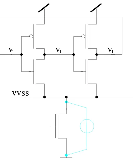
After a circuit block has been cut-off, it reaches a certain steady state. This state has to be known in order to estimate the remaining leakage current. Usually the total transistor width in the logic block is much larger than the width of the switch device. Hence the potential of the virtual power-rail(s) has to change until the leakage current of the logic block is equal to the leakage of the switch. Figure 1 shows an equiv-alent circuit which models an n-block switched circuit. The cross coupled inverters are dimensioned very large in order to describe a large logic block with half of the nodes at logic high level and half of the nodes at logic low level. This sim-ple equivalent circuit has a low transistor count, thus even large logic blocks can be modeled efficiently. The cross cou-pled inverter structure neglects interface effects between a power switched circuit block and the surrounding circuitry. Thus other models have to be used if these effects are to be investigated. In order to find the final state after switching-off a circuit block, the potential of the virtual power rail has been ramped up. The current through the switch device as well as the total current in the logic is given in Fig. 2. The steady state of the idle system is determined by the intersec-tion of the two current voltage characteristics of the switch and the logic. Depending on the transistor widths and thresh-old voltages, the potential of the virtual power rail (vvss) moves versus the non switched power rail (vdd). In typical n-block switched circuits thevvss potential as well as the potential of all internal signal nodes charges up to a value slightly below the vdd potential. Thus all transistors operate in subthreshold region:
Ip=I0pexp
vdd−v
1+vtp ηvT
1−exp
v
1−vdd
vT
228 S. Henzler et al.: Theory of circuit block switch-off
Book: Kleinheubacher Berichte MS No.: KH2003-A-00112
First author: Stephan Henzler 7
v
1v
1vvss
v
1Figure 1.Equivalent circuit to model a large power switched circuit block. Interface effects between the circuit block and the surrounding circuitry are neglected by this circuit. A voltage source between the virtual power rail and ground can be used to determine the current voltage characteristic of the circuit block and the switch device.
0 0.2 0.4 0.6 0.8 1 1.2
10−13 10−12 10−11 10−10 10−9 10−8 10−7 10−6
vvss−potential [V]
leakage current [A]
Figure 2.Simulated leakage-voltage-characteristic of several logic circuits with different total transistor widths and subthreshold characteristic of two switch devices with low and high threshold voltage. The intersection of these curves determines the stationary state after block deactivation.
Fig. 1. Equivalent circuit to model a large power switched circuit block. Interface effects between the circuit block and the surround-ing circuitry are neglected by this circuit. A voltage source between the virtual power rail and ground can be used to determine the cur-rent voltage characteristic of the circuit block and the switch device.
In=I0nexp
v1−vvss−vt n ηvT
1−exp
−v1−vvss
vT
(2)
Is=I0sexp
−
vt s ηvT
1−exp
−vvss
vT
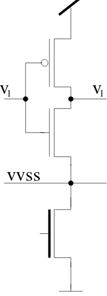
(3) Hence the equivalent circuit of Fig. 3 can be used to derive an analytic expression for the steady state. The total logic width is assumed to be much larger than the width of the switch de-vice. Thus Fig. 2 states that the potential of the virtual power rail is slightly below vdd. Therefore thevvss dependency of the subthreshold current in the switch device can be ne-glected and the switch threshold voltagevt sis approximated
by the switch threshold voltage at maximum drain-to-source voltageVdsswitch=vdd. As the deviation of thevvsspotential with respect tovdd is small, the potentialV1of the signal nodes is also slightly belowvdd. Thus a perturbation ap-proach can be used to describe these voltages:
V1=vdd−1V1 0< 1V1vdd (4)
vvss=V1−1V2 0< 1V2vdd (5)
solving the linear equation system 1-3 results in
1V11,2=1 2ηvT
−1± v u u u t
1+4
η I0s I0p
exp
−vt s+vtp
ηvT
| {z }
>1 (6)
v
1v
1vvss
v
1Figure 1.Equivalent circuit to model a large power switched circuit block. Interface effects between the circuit block and the surrounding circuitry are neglected by this circuit. A voltage source between the virtual power rail and ground can be used to determine the current voltage characteristic of the circuit block and the switch device.
0 0.2 0.4 0.6 0.8 1 1.2
10−13 10−12 10−11 10−10 10−9 10−8 10−7 10−6
vvss−potential [V]
leakage current [A]
Figure 2.Simulated leakage-voltage-characteristic of several logic circuits with different total transistor widths and subthreshold characteristic of two switch devices with low and high threshold voltage. The intersection of these curves determines the stationary state after block deactivation.Fig. 2. Simulated leakage-voltage-characteristic of several logic
cir-cuits with different total transistor widths and subthreshold charac-teristic of two switch devices with low and high threshold voltage. The intersection of these curves determines the stationary state after block deactivation.
1V21,2=1
2ηvT −1±
s
1+4
η I0s I0n
exp
v
t n−vt s ηvT
!
(7) The upper solution is physical meaningful and for
I0sI0p, I0nEq. (6) and Eq. (7) can be approximated by 1V1=vT
I0s I0p
exp
−vt s+vtp
ηVT
(8)
1V2=vT I0s I0n
exp
v
t n−vt s ηVT
(9) These equations state that the voltage difference of the signal- andvvss-nodes decreases exponentially with increas-ing switch threshold voltage and linear with decreasincreas-ing width ratio Ws
Wlog.
3 Leakage reduction ratio
The target of any CBSO scheme is the reduction of the age current of unused circuit blocks. The quality of this leak-age reduction can be quantified by the leakleak-age reduction ratio (LRR):
LRR:= I
no switch
L
ILswitch off
(10)
ILno switchis the total leakage current of the considered cir-cuit block if no cut-off switch is used andILswitch offis the remaining leakage current of this circuit block if a cut-off switch is added and turned off. Without cut-off switch, the leakage of an arbitrary static CMOS circuit can be calculated according to
ILno switch=X
{LV}
WPeffIp0e
vtp
ηvT +WneffjTn
+
X
{HV}
WneffIn0e
vtn
ηvT +WpeffjTp
S. Henzler et al.: Theory of circuit block switch-off 229
Book: Kleinheubacher Berichte
MS No.: KH2003-A-00112
First author: Stephan Henzler
8
vvss
v
1v
1Figure 3.
Reduced equivalent circuit to determine the stationary cut-off state analytically.
sel
VVss
C
3C
1T
nT
pT
sVVss
C
3C
1C
2T
nT
pC
2Vdd
Vdd
Figure 4.
Equivalent Circuit of a large logic block with internal capacities
0 0.1 0.2 0.3 0.4 0.5 0.6 0.7 0.8 0.9 1
x 10−5
0 0.2 0.4 0.6 0.8 1 1.2
1.4x 10
−10
time after deactivation [s]
inertial current [A]
simulated inertial current
approximation of inertial current
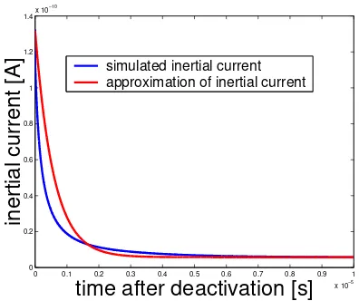
Figure 5.
Time dependence of inertial current and its approximation by an exponential function
Fig. 3. Reduced equivalent circuit to determine the stationary cut-off state analytically.
{Lv}describes the set of gates with a low output level and
{Hv}the disjoint set of gates with a high output level.In0 and Ip0 respectively describe the subthreshold leakage per transis-tor width andjTn andjTp refer to the gate tunneling currents per transistor width. (Assuming all transistors have the same channel length.) Averaged over all system states, the leakage current can be approximated by a common effective logic widthWLeff:
ILno switch≈ 1 2W
eff L
Ip0e
vtp
ηvT +In0e−ηvTvtn +jTn+jTp
(12) In an n-block switching scheme, the virtual ground potential charges up to a voltage slightly belowvdd. Thus the residual leakage current can be estimated by
ILswitch off=Ws
Is0e−ηvTvts +jTs (13)
Insertion of Eqs. (12) and (13) into (10) results in the LRR of the n-block switching scheme.
4 Power-down process
When a circuit block is not used it can be turned off by a cut-off switch. As the circuit block includes inner capacities, the
vvss
Figure 3.Reduced equivalent circuit to determine the stationary cut-off state analytically.
sel VVss
C3
C1
Tn
Tp
Ts
VVss
C3
C1
C2 Tn
Tp
C2
Vdd Vdd
Figure 4.Equivalent Circuit of a large logic block with internal capacities
0 0.1 0.2 0.3 0.4 0.5 0.6 0.7 0.8 0.9 1
x 10−5
0 0.2 0.4 0.6 0.8 1 1.2 1.4x 10
−10
time after deactivation [s]
inertial current [A]
simulated inertial current approximation of inertial current
Figure 5.Time dependence of inertial current and its approximation by an exponential function
Fig. 4. Equivalent Circuit of a large logic block with internal capac-ities
leakage current does not collapse instantaneously. Instead, as shown in Fig. 5 there is a smooth transition between the active leakage and the residual leakage in idle mode. Dur-ing this transition thevvss rail as well as the internal signal nodes charge up to a potential usually slightly below vdd. Figure 4 shows the equivalent circuit introduced in Sect. 2 and its internal capacities. The capacities labeled byC2 rep-resent the capacity of each signal node versus thevdd-rail and the capacities labeled by C3 represent the capacitance with respect to the virtual ground rail. Hence the collapsing supply current charges theC1andC2capacitances. The ca-pacitiesC3however are discharged. Thus the intrinsic energy dissipationWintrdue to charging the inner capacities can be estimated by
Wintr=vdd2
X
C1+
X
{Lv}
C2−
X
{Hv}
C3
!
≈vdd2
X
C1+
1 2
X
C2−
1 2
X
C3
=1 2vdd
2X
(2C1+C2−C3) (14)
When the circuit is turned on again, about half of the sig-nal nodes keep a logic high level and hence the energy
Wboot,cap=12vdd2C3is dissipated in order to charge up the
C3capacitances associated to these nodes.
In order to estimate the minimum timeTminfor which it is useful to turn off the circuit block, the collapse of the supply current after the switch is turned off has to be modeled prop-erly. The model of this current has to be accurate but also simple enough to be used in analytic expressions. The leak-age current after turning off the system can be decomposed according to
iL(t > toff)=iLoff+iinertia(t ) lim t−toff→∞
iinertia→0 (15)
230 S. Henzler et al.: Theory of circuit block switch-off
vvss
Figure 3.Reduced equivalent circuit to determine the stationary cut-off state analytically.
sel VVss
C3
C1
Tn
Tp
Ts
VVss
C3
C1
C2
Tn
Tp
C2
Vdd Vdd
Figure 4.Equivalent Circuit of a large logic block with internal capacities
0 0.1 0.2 0.3 0.4 0.5 0.6 0.7 0.8 0.9 1 x 10⁻⁵ 0
0.2 0.4 0.6 0.8 1 1.2 1.4x 10
−10
time after deactivation [s]
inertial current [A]
simulated inertial current approximation of inertial current
Figure 5.Time dependence of inertial current and its approximation by an exponential function
Fig. 5. Time dependence of inertial current and its approximation by an exponential function
byRt∞
offiinertia(t ) dt. If the leakage current was collapsing
in-stantaneously the time which one has to wait in order to save the power penalty due toWintris given by
Tinertiaeff =
R∞
toffiinertia(t ) dt ILon−ILoff
= Wintr
vdd ILon−ILoff (16)
This time should be called effective inertial time. A simple approximation for the inertial current is the exponential func-tion:
iinertiaapprox=
ILon−ILoff
exp
−t−toff
τ
(17) It is suggestive to determine the time constantτ such that the total energy dissipation due to the exponential function is equal to the real energy consumption. Equating this postula-tion results inτ=Tinertiaeff .
5 Minimum powerdown time
Turning a circuit block off and on causes not only intrinsic energy dissipationWintrbut also extrinsic lossesWextr. These losses consist of losses in the switch device, in the switch driver and in the power-down-logic. Additionally there are losses during the power-up process (power-up glitches,
Wboot,cap). Summing up all these energy dissipations re-sults in the total energy penalty due to the power switching:
Wtot=Wintr+Wextr.
The power saving due to the power switching at timet >toff can be calculated by
Psave(t )=(1IL−iinertia(t )) vdd 1IL:=ILon−I off
L (18)
If the circuit block is switched on again at timetoff+T the energy penalty and the saved energy are given by
Wloss=vdd
Z T+toff
toff
iinertia(t ) dt+Wextr (19)
Wsaved=vdd
Z T+toff
toff
1ILdt (20)
Equating these two expressions results in the so called energy equivalent powerdown timeTeeq which describes the
mini-mum time for which it is useful to switch the circuit block off under power considerations:
Wextr
vdd =1IL
Teeq+Tinertia
exp
− Teeq
Tinertia
−1
(21) If the extrinsic losses are large,TeeqTinertiaand therefore
Teeq ≈ Wextr
vdd1IL
+Tinertia (22)
Although this time is the main contributor to the minimum powerdown time Tminthere are additional terms due to the signal propagation delay in the power-down-logic and the switch driver. Additionally, there is a certain settling time
Tpower onCB before the circuit block can be used after block ac-tivation. The minimum power-down time is the sum of all these contributors:
Tmin=2Ttotswitch+Teeq+Tpower onCB . (23)
6 Dynamic behaviour of CBSO-systems
As the cut-off device in a CBSO-system has a finite on-resistance, the supply current through the logic block causes a voltage drop across the switch. Hence the effective sup-ply voltage is reduced and the signal propagation delay in the circuit increases. The voltage-delay dependence of static CMOS gates can be derived by analytic MOSFET models like the alpha-power-law:
d ∝ vdd
(vdd−vt h)α
(24) In this equationvddis the nominal supply voltage,vt his the
threshold voltage andαis a technology dependent coefficient with values between 1 and 2. As the whole supply current of a power switched circuit flows across the cut-off switch, the delay degradation depends on the switching activity of all gates assigned to the switch. Therefore not only the time critical paths but the ensemble of all gates which switch their outputs while the signal propagates through the critical paths determine the overall delay of the circuit. Furthermore, the voltage-delay characteristic Eq. (24) is nonlinear and hence it is not a trivial task to determine the optimum dimensioning of the switch device. A large switch transistor reduces the delay degradation but suffers from large area consumption and poor leakage supression. In order to estimate the delay degradation for a given circuit if a certain cut-off switch is added, the supply current profile of the circuit without off switch is assumed to be known. The addition of a cut-off switch causes delay degradation but does not affect the logic function of the circuit. Hence the switching events are the same whether a cut-off switch is inserted or not and the current profiles of the two cases are similar.
S. Henzler et al.: Theory of circuit block switch-off 231 during the output transition and the dynamic current which
charges the load capacitance. As the effective supply volt-age is reduced due to the voltvolt-age drop across the switch de-vice, the charge which is necessary to charge the load capac-ity is reduced. The voltage swing of the virtual ground line in a n-block-switching scheme is small in order to keep delay degradation low. Hence the charge on the nonlinear load ca-pacitance of an arbitrary gate can be estimated by linear tay-lor approximation:Q(v)=c(v)vdescribes the dependence of the charge on this capacity on the voltage. In the vicinity of
vdd,c(v)is assumed to be a weak function ofv. If the effec-tive supply voltage is reduced byvvss, the charge necessary to charge up the load capacity can be expressed by
Q(vdd−vvss)=Q(vdd)−dQ
dv(vdd)vvss
=c(vdd)vdd−c(vdd)vvss−dc
dv(vdd)vdd vvss
≈c(vdd)[vdd−vvss]. (25)
A similar approach can be done for the charge that is injected into the virtual power rail due to short circuit and leakage currents. Hence the supply current of a logic circuit can be decomposed according to
i(t )= dq
dt =ζ (t )vdd(t ) (26)
into an effective conductivityζ (t )and the momentary sup-ply voltage. If there is no cut-off switch the supsup-ply voltage is constant andζ is given byζ (t )=i(t )
vdd. Using this expression
the charge which is injected into the ground node during the time interval [t;t+dt] can be expressed bydq=ζ (t )dt vdd. Assuming that the supply current profile of a large circuit block is given and assuming further that this current profile results from many discrete switching events, this current pro-file can be partitioned into small current pulses of widthdτ. The distinct current pulses are shaped in the following way in order to estimate the current profile of the circuit with cut-off switch: The charge which is injected into the virtual ground node is reduced due to the reduced effective supply voltage. Henceζ has to be multiplied by this effective supply
volt-agevdd−vvss(t ). Moreover the time interval during that
this charge is injected is stretched with respect to the time interval if there was no switch device. Assumei(τ )is the current profile of a given circuit block without cut-off switch for a certain input transition. The dynamic of this circuit is described in the time variableτ. The current profilei(t )of the circuit block with cut-off switch has to be determined by shaping the given profile. The time variablet describes the dynamic of the power switched circuit block. The charge which is injected into the virtual ground node during the time interval [t;t+dt] is given by
dq(t )=ζ (τ (t ))·[vdd−vvss(t )]dτ (t ) (27)
The relation between the two infinitesimal time elementsdt
anddτ is given by the normalized supply voltage dependent delay degradationδ(v)of a CMOS gate:
dt=δ (vdd−vvss(t )) dτ (28)
0 0.5 1 1.5 2 2.5
x 10−9 −1
0 1 2 3 4 5 6x 10
−3
time [s]
measured vss−current [A]
0 0.5 1 1.5 2 2.5
x 10−9 −0.005
0 0.005 0.01 0.015 0.02 0.025 0.03 0.035 0.04 0.045
time [s]
virtual ground potential [V]
solving deq−system directly circuit simulation
Figure 6.Example for a current supply-current-profile and the resulting potential of the virtual ground line. The congruence of the curve determined by analog circuit simulation and the direct solving of the derived deq-system is very good.Fig. 6. Example for a current supply-current-profile and the
result-ing potential of the virtual ground line. The congruence of the curve determined by analog circuit simulation and the direct solving of the derived deq-system is very good.
Combining Eqs. (27) and (28) results in an expression for the current profile in thetdomain which can be inserted into the Kirchhoff current equation of the virtual ground node:
dQ
d vvssvvss(t )˙ +I (vvss(t ))
=ζ (τ (t ))δ−1(vdd−vvss(t ))[vdd−vvss(t )] (29)
dt=δ(vvss)dτ (30)
Solving this system of ordinary differential equations results in an estimation of the current profile of the circuit with current switch. The nonlinear functions qc=Q(vvss) and iR=I (vvss)describe the charge on thevvss-capacitance and
Thus many different input transistions, switch sizes or switch device types can be examined by this fast compact simulation methodology.
7 Conclusion
In this paper we have described analytically the bahaviour of a power switched circuit block during and after the block deactivation. The minimum power down time has been de-fined and the main contributors have been derived. Finally a fast analytic methodology to estimate the influence of a cut-off switch on the dynamic performance of a circuit has been proposed.
tional Conference on Very Large Scale Integration of System-on-Chip, 2003.
Mutoh, S., Douseki, T., Matsuya, Y., Aoki, T., Shigematsu, S., and Yamada, J.: 1-V Power Supply High-Speed Digital Circuit Technology with Multithreshold-Voltage CMOS, IEEE Journal of Solid-State Circuits, 30, 8, 847–854, 1995.
Kawaguchi, H., Nose, K., and Sakurai, T.: A Super Cut-Off CMOS (SCCMOS) Scheme for 0.5-V Supply Voltage with Picoampere Stand-By Current, IEEE Journal of Solid-State Circuits, 35, 10, 1498–1501, 2000.
Min, K., Kawaguchi, H., Sakurai, T.: Zigzag Super Cut-off CMOS (ZSCCMOS) Block Activation with Self-Adaptive Voltage Level Controller: An Alternative to Clock-Gating Scheme in Leakage Dominant Era, IEEE Solid State Circuits Conference, 2003. Meer, P. R. and Staveren, A.: New standby-current reduction