INTRODUCTION
The synthesis and characterization of zinc sulphide via different techniques have attracted considerable attention due to their potential application prospects in thin film devices such as pholuminescent and electroluminescent devices and more recently as n-type window layer heterojunction solar cell¹. The II-VI group of sulphides has distinctive features of high ionicity (compared to Si, Ge and III-V compounds), large band gap, and transparency in the visible region. In this regard zinc sulphide (ZnS) deserves a special mention because of its large optical band gap, in fact, the highest (>3.6 eV) among all II-VI compound semiconductors. Accordingly, different physical and chemical techniques have been utilized to grow ZnS thin films. These include sputtering, evaporation, molecular beam epitaxy, chemical vapor deposition, atomic layer epitaxy², chemical bath deposition (CBD)3-4 and many others. One of the relatively less used and less studied techniques is SILAR (Successive ionic layer adsorption and reaction) In SILAR technique thin films are obtained by
Material Science Research India Vol. 5(2), 447-452 (2008)
Preparation of ZnS thin film by Silar
S. DATTA ROY and P. MITRA*
Department of Physics, The University of Burdwan Golapbag, Burdwan - 713 104 (India).
(Received: September 09, 2008; Accepted: October 17, 2008)
ABSTRACT
Polycrystalline zinc sulphide (ZnS) thin film was synthesized using chemical bath deposition (CBD) technique. The films are phase pure and polycrystalline with crystallite size approximately 12 nm. The crystallite size was measured using X-ray line broadening method. The electrical characterization was carried out using conventional DC two-probe technique. An activation energy barrier value of 0.60 eV was observed, which can be associated with deep acceptor levels due to excess zinc atoms.
Key words: Zinc sulphide, polycrystalline thin film, CBD.
EXPERIMENTAL Material and methods
Zinc sulphide thin film was deposited on microscope glass slide substrates. The substrate was cleaned prior to deposition process. It was kept overnight in chromic acid. The chromic acid solution was prepared by adding 70 gm. K2Cr2O7 in 320 cc distil water. Finally 120 cc sulphuric acid (99% H2SO4)was added to the mixture for complete dissolution of K2Cr2O7. This was followed by rinsing the substrate in distilled water and ultrasonic cleaning in equivolume mixture of acetone and alcohol in an ultrasonic cleaner. The substrate was tightly held in a holder so that only a requisite area for film deposition was exposed. The film thickness was measured gravimetrically6 by weighing the substrate before and after deposition in an electronic balance and taking the theoretical density of ZnS. For preparation of ZnS thin film, 0.1 M solutions of zinc acetate [Zn (CH3COO)2] and thiourea [SC (NH2)2] in deionized water were used. Ammonia (NH4OH) was used as complexing agent. Addition of ammonia in zinc acetate solution initially leads to as white precipitate possibly due to the formation of Zn (OH)2 . Further addition of ammonia leads to a transparent solution. The pH of the ammonium zincate bath was maintained at ~11.0 by adding ammonia in order to get a stable transparent solution. Since ammonia is volatile, excess of ammonia is required for getting a stable solution for a reasonably long time. Similarly, the pH of thiourea bath was adjusted to ~9.0 by adding ammonia solution. The pH measurement was carried out in a Systronics pH meter (Model 335). Both the baths were kept at room temperature. Ubale et al ¹ used chemical bath deposition (CBD) technique to deposit ZnS thin film by adding thiourea solution in zinc acetate solution. The pH of the mixture was maintained between 9 and 10 in their work.
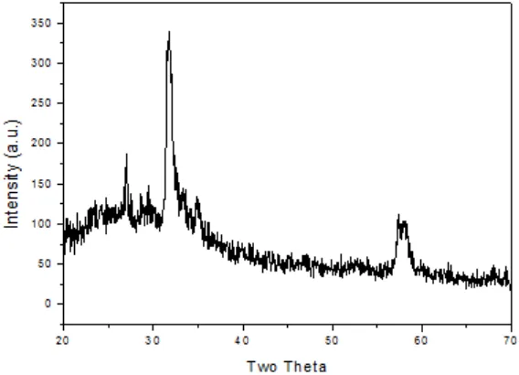
X-ray diffraction (XRD) with CuKα radiation (λ=1.5418 Å) was used for str uctural characterization and phase identification of the deposited ZnS films in a X-ray diffractometer (XRD). Scanning electron microscopy (SEM) was used to illustrate the formation of crystallites on the film surface.
The electrical characterization of the deposited films was carried out in a closed tube furnace by monitoring the variation of electrical resistance (R) as a function of temperature (T) using the conventional DC two-probe technique. The temperature was controlled using a temperature controller and the resistance values were measured using a digital multimeter (DMM). The range of temperature investigated was room temperature to 150oC with a control accuracy of (±)1oC. Conducting silver (Ag) paste was used for electroding. Approximately 20 mm long and 1 mm wide Ag contacts, separated by 5 mm, were made on ZnS films (3 x 2.5 cm2) for electrical measurements. The width of the electrodes was approximately 1 mm. The conducting silver paste was cured at 200oC for this purpose. Copper (Cu) wires were connected from the electrodes to the resistance-measuring instrument.
RESULTS AND DISCUSSIONS Film deposition
The cleaned solution was first dipped in zinc acetate solution and then in thiourea solution. In an alkaline medium, zinc acetate acts as the source of Zn2+ ions and thiourea as the source of S2- ions¹. The reaction on the substrate can be represented as
The film thickness, measured gravimetrically, was found to be approximately 1.0 µm for 200 dipping in the two baths. The dipping time in each bath was 5 seconds.
Structural characterization
Table 1
Peak Position d-values Miller indices Relative intensity
No. (2θθθθθ) (hkl) (I/Io)
1 27.00 3.30 (100) 55
2 30.75 2.95 (101) 100
3 58.2 1.63 (112) 31
4 58.3 1.59 (201) 30
Table 2
Peak No. Position (2θθθθθ) Intensity FWHM
1 28.48 100 0.156
2 47.32 52 0.196
3 56.14 29 0.212
miller indices of the reflecting planes obtained from XRD pattern for ~1 µm thick film.
Relative intensity is calculated by taking the highest intensity at 30.75o as 100
( )
o I . The intensity of other peaks is normalized with respect to this value
o
I I ⎛ ⎞ ⎜ ⎟
⎝ ⎠. The crystallite size was calculated
by the X-ray line broadening method using the Scherrer formula8.
cos
k
D
λ
β
θ
=
where λ is the wave length of radiation used (CuKα in this case),
k
is the Scherrer constant, β is the full width at half maximum (FWHM) intensity of the diffraction peak for which the particle size is to be calculated, è is the diffraction angle of the concerned diffraction peak and D is the Crystallite dimension (or par ticle size). Assuming k=0.89, which corresponds to spherical crystallites, the average particle size calculated using Scherrer formula for ~1.0 µm thick film is approximately 12 nm.While calculating the particle size, the instrumental broadening was taken into account. The instrumental broadening (βi) also contributes to the observed or measured broadening (βO)6. Thus
Fig. 1: XRD pattern of ~1.0 mm thick ZnS film
the observed broadening is generally represented as βo=β+βi , where β is the actual broadening arising solely from particle size. In other words β is the corrected line width at half-peak intensity. Diffraction data from silicon (Si) powder was used to measure the instrumental broadening. The broadening in this case is due to instrument and crystallite broadening is almost negligible. Table shows the values of FWHM for the three highest intensity silicon peaks (XRD pattern for Si is not shown for brevity).
A plot of 2θ vs FWHM for standard silicon is drawn. The values of observed broadening (βo) for ZnS peaks are calculated at the of ZnS. The values of instrumental broadening βi at these 2θ values are then evaluated form the plot of vs FWHM for standard Si. This value is then deducted from observed broadening to get the par ticle size broadening9-10.
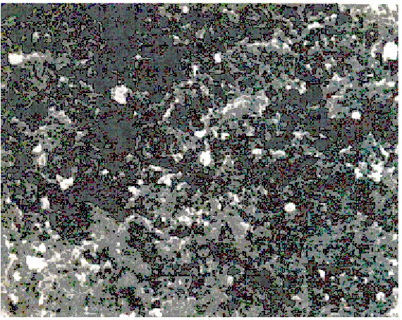
The SEM of ~1.0 µm of ZnS thin film on glass substrate is shown in Fig. 2. The formation of sub-micrometer crystallites distributed more or less uniformly over the surface is evident from the figure. Some holes indicating porosity and agglomeration of small crystallites also seem to be present in
certain regions on the film surface.
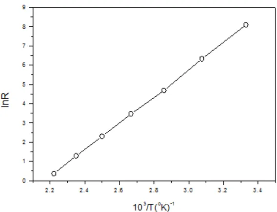
Electrical resistance vs. temperature for SnS thin film
Fig. 3 shows the variation of resistance with temperature. Resistance was measured in kilo-ohms In Rvs 10³/T and vs. is plotted in figure. It is observed that resistance decreases with increasing temperature, suggesting the semiconducting behavior of ZnS film.
The activation energy was determined by using the equation
where R is the resistance at temperature T, Ro, is a constant, Ea is the activation energy and k is the Boltzmann constant
Therefore
Fig. 3: Temperature dependence of resistance for ZnS film
Knowing R1, R2, T1, T2 and using the known value of
k
,E
a is calculated.The activation energy value for the present ZnS film is 0.60 eV. Ubale et al ¹ reported activation barrier values of 1.29 eV for 72 nm thick films and 0.81 eV for 332 nm thick films. It was suggested that increase of thickness leads to decrease in resistivity and lowering of activation energy. Thus
the observed value of 0.60 eV is on the lower side and is possibly due to large thickness (~1.0 µm) of the film compared to those reported by Ubale et al.¹.
ACKNOWLEDGEMENTS
The authors acknowledge DSA III, Dept. of Physics, for providing the some of the instrumental facilities for carrying out the work. One of the authors (PM) gratefully acknowledge the financial support provided by UGC (India) in the form of a minor project (F. No. 32-65/2006 (SR).
REFERENCES
1. Ubale A., and Kulkarni D., Bulletin of Materials Science, 28: 447 (2005).
2. Lindroos S., Kanniainen T., M. Leskela and E. Rauhala, Thin Solid Films 263: 79 (1995). 3. J. M. Dona and J. Herrero, Bulletin of
Materials Science, 139: 2810 (1992). 4. D. Johnston, I. Forbes, K. T. Ramakrishna
Reddy and R. W. Miles, J. Mat. Sc. Lett. 20:
921 (2001).
5. S. Lindroos, Y. Charreire, D. Bonnin and M. Leskela, Materials Research Bulletin 33: 453 (1998).
6. S. Mondal and P. Mitra, Materials Science Research India, 5: 67 (2008).
Diffraction Data, Swarthmore, PA, card no. 36-1450 (1995).
8. B. W. Sanders and A. Kitai, Chem. Mater., 4: 1005 (1992).
9. Klug. H and Alexander L, X-ray diffraction
procedures for polycr ystalline and amorphous materials, Wiley, New York, 618 (1974).