_____________________________________________________________________________________________________
Wirebond Solution of Semiconductor IC Package
through Modeling and Simulation
Frederick Ray I. Gomez
1*, Anthony R. Moreno
1and Jonathan C. Pulido
11
Departmentof New Product Development and Introduction, STMicroelectronics, Inc., Calamba City, Laguna, 4027, Philippines.
Authors’ contributions
This work was carried out in collaboration among all authors. All authors read and approved the final manuscript.
Article Information
DOI: 10.9734/JERR/2019/v7i316970
Editor(s):
(1)Dr. Y. Thiagarajan, Assistant Professor, Sri Venkateshwaraa College of Engineering and Technology, India.
Reviewers:
(1) Yuan-Tsung Chen, National Yunlin University of Science and Technology, Taiwan. (2) Adel H. Phillips, Ain-Shams University, Egypt. (3) Himanshu Dehra, India. (4) Boyan Karapenev, Technical University of Gabrovo, Bulgaria. Complete Peer review History:http://www.sdiarticle4.com/review-history/51870
Received 01 August 2019 Accepted 03 October 2019 Published 14 October 2019
ABSTRACT
This technical paper presents a study of wirebond selection highlighting the package electrical modeling and simulation done for semiconductor integrated circuit (IC) leadframe package (hereinafter referred to as Device Z) with different wirebond configurations: Gold 2N 1.3 mil, Gold 4N 1.3 mil, Copper 1.3 mil, Copper 1.2 mil, Copper 1.1 mil and Copper 1.0 mil. Package design, modeling and simulation are essentially important in the early stage of the package development, particularly at the package feasibility phase.
As Device Z is previously assembled with Gold 4N 1.3 mil wirebond configuration, this technical paper focused in determining the best alternative for Gold 4N 1.3 mil in wirebonding through package modeling and simulation. Statistical analysis reinforced the study to verify the trend and to check if there is significant statistical difference in the resistance, inductance and capacitance (hereinafter referred to as RLC) performance of the device given the different wirebond configurations. Cost analysis was crucial to determine the cost impact of using different wires. Prioritizing the wirebond thickness and cost without sacrificing the electrical performance, Copper 1.1 mil would be the most suitable replacement for Gold 4N 1.3 mil wirebond configuration. However, since Copper 1.1 mil is not yet available in the market, Copper 1.2 mil could be used,
with better electrical parameters. In addition, Copper wire offered significant cost improvement over its Gold counterpart. Computed cost per unit of Copper 1.3 mil is just 6% of the total cost of the Gold 4N 1.3 mil – that is 94% cost savings. Ultimately, Copper wire technology offers significant cost savings and could pave the way for more businesses in the plant.
Keywords: Package electrical modeling; simulation; wirebond; leadframe; semiconductor.
1. INTRODUCTION
With the latest technology and continuing trends, increasing market competition, and accelerating development in semiconductor industry [1-2], one should be flexible, resourceful and relatively quick in adapting to change, for the business to keep going. This is a major challenge for any semiconductor and technology company in order to maintain its competitive market value and
position. Contrariwise, failure to provide
customer expectation will result in eventual business failure.
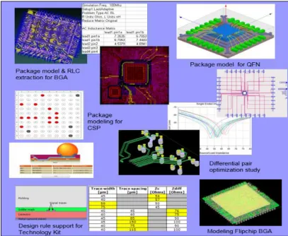
Semiconductor package design, modeling and simulation are critical tools that help realize faster time-to-market development of semiconductor package. These capabilities play vital roles in the early stage of the package development, particularly at the package feasibility phase. Modeling, characterization and simulation are comprehensively used to evaluate and anticipate
the new package performance and behavior, i.e.
electrical performance and thermo-mechanical behavior. Fig. 1 illustrates examples of package
models used for electrical modeling,
characterization, and simulation.
A semiconductor integrated circuit (IC) device packaged in a standard leadframe configuration (hereinafter referred to as Device Z) previously utilized Gold 4N 1.3 mil wirebonding for power applications. However, the price of Gold (Au) has greatly increased in recent years, fueling the demand for high-volume wirebonding using other alternative like that of the Copper (Cu) wire, which can lead to significant cost savings due to lower raw material cost. Copper wire also offers better or higher electrical conductivity (reciprocal of resistivity) than its Gold counterpart, allowing more signals to flow in the circuit with less electrical loss at a given time. The development of Copper wire is one important achievement in the semiconductor industry, providing cost-efficient devices for wide range of power applications [3-4]. Moreover, one critical part of the development is at the package feasibility
level wherein package design, modeling,
characterization, and simulation take important roles.
Package electrical modeling study is essential to determine the package behavior and effect of different wirebond (or wirebond) configurations on Device Z: Gold 2N 1.3 mil, Gold 4N 1.3 mil, Copper 1.3 mil, Copper 1.2 mil, Copper 1.1 mil, and Copper 1.0 mil. As Device Z is previously assembled with Gold 4N 1.3 mil wirebond configuration, the ultimate goal of the study is to eventually determine the best alternative for Gold 4N 1.3 mil in wirebonding, prioritizing the wire size and cost without sacrificing the electrical performance.
2. REVIEWOFRELATEDLITERATURE
Semiconductor package modeling,
characterization and simulation are essentially carried out to evaluate, quantify and anticipate the new package performance and behavior. In electrical or electronic circuits and components, parasitic or inherent elements particularly the parasitic resistance, inductance and capacitance (RLC) should be minimized as these elements are unavoidable and not desirable for the components to have for its intended purpose. For instance, a resistor in Fig. 2 is designed to exhibit resistance, but also possesses unwanted parasitic inductance and capacitance [5]. Since parasitic RLC of the device cannot be completely eliminated, package designers will always strive to minimize it.
Different wirebond materials are available in the market, with each having their particular
electrical properties. Package electrical modeling is important to analyze the effect of different wires on the overall electrical performance of the semiconductor package.
Fig. 2. Equivalent RLC circuit of a resistor
2.1 Package Electrical Parameters
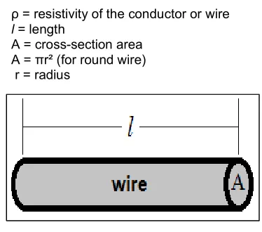
As wirebond is a conductor, equivalent
resistance of the wire could be computed using the expression in Eq. (1) for the sample wire in Fig. 3.
R = ρ l / A (1)
where
ρ = resistivity of the conductor or wire
l = length
A = cross-section area A = πr² (for round wire) r = radius
Fig. 3. Straight-wire conductor or wire, for resistance computation
Inductance value could be estimated using Eq. (2) for the straight-wire conductor. Increasing the diameter of a straight-wire conductor, like that of the wirebond, results in lower inductance.
L = 0.2l ∙ [ ln ( 4l / d ) – 1 ] (2)
where
L = inductance in µH
Eq. (3) gives the simplified expression for the capacitance of a thin straight wire, for this case the wirebond.
C = (2επl) / [ln (l / r)] (3)
where
ε = absolute permittivity of the dielectric material
l = length of the conductor/wire r = radius of the conductor/wire
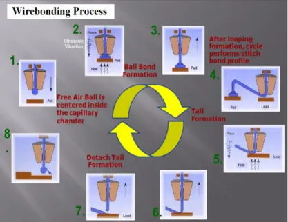
2.2 Wirebonding Process Overview
Wirebonding is the method of making electrical connections between the silicon die and its
packaging during semiconductor device
assembly manufacturing, using very fine bonding wires. Fig. 4 illustrates the overview of the assembly wirebonding process. It is worth noting that wirebonding process varies also with the product and the technology [1,4,6]. Wirebonding
could also be used to connect any
semiconductor device or integrated circuit (IC) to other electronic device or to connect from one printed circuit board (PCB) to another.
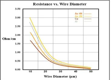
2.3 Copper Wire versus Gold Wire
Gold (Au) wire has been the most widely used wire in wirebonding process. However, in recent years the price of Gold has greatly increased, fueling the demand for high-volume wirebonding using Copper wire, which can lead to significant cost savings due to lower raw material cost. Aside from being cost-efficient, Copper wire exhibits lower resistance [3,4,7] in Fig. 5, which allows more signals to flow and less electrical loss at a given time.
With the discussion on Copper wire vs Gold wire, the challenge now is to determine the suitable replacement for Gold 4N 1.3 mil in wirebonding, based on the electrical performance through package modeling and simulation.
Fig. 5. Wirebond resistance versus size [7]
3. METHODOLOGY
Different wirebond models exist in package electrical modeling depending on the complexity of the design. Wirebond 3D model (cross-sectional view) in Fig. 6 was used for the study of Device Z, with parameters in Table 1 initially determined by the stakeholders.
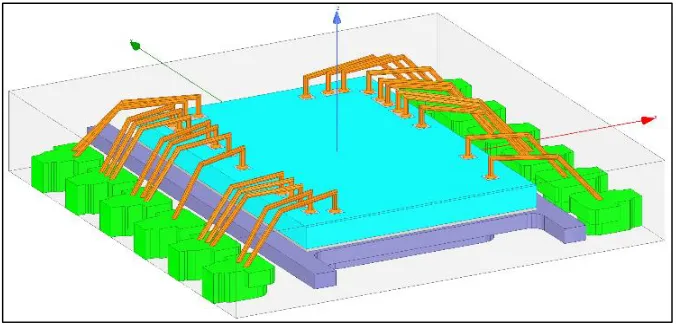
The electronic design automation (EDA) software tool [8] used has the option to run Perl script that enables faster 3D model generation from 2D drawing of another computer-aided design (CAD) software tool [9] in Fig. 7 to the 3D equivalent model in Fig. 8.
To minimize wirebond electrical loss of Device Z and to have better electrical performance, RLC should be kept at minimal. As earlier discussed, the objective of the package electrical modeling study is to determine the package behavior and effect of different wirebond configurations on the device.
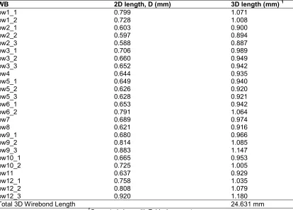
The models were analyzed at DC (direct current) for the DC resistance measurement and at AC (alternating current) with sample application frequency of 1.65 MHz for the RLC extraction. Total 3D wire length is computed based on the 2D length in Table 2 and the 3D wirebond parameters in Table 1.
Table 1. Wirebond 3D model parameters
Wirebond parameter Value
Material Gold 2N Gold 4N Copper
Conductivity, σ 31 x 106 43 x 106 58 x 106 S/m
Size/Diameter 1.3 mil 1.3 mil 1.0/1.1/1.2/1.3 mil
2D length, D See Table 2
Alpha angle, α 90 degrees
Span length, s 60% of D
Loop height, h1 0.130 mm
Die + die attach thickness, h2 0.170 mm
Fig. 7. Mount and bonding diagram 2D model of device Z
Table 2. Wirebond 3D length
WB 2D length, D (mm) 3D length (mm) 1
bw1_1 0.799 1.071
bw1_2 0.728 1.008
bw2_1 0.603 0.900
bw2_2 0.597 0.894
bw2_3 0.588 0.887
bw3_1 0.706 0.989
bw3_2 0.660 0.949
bw3_3 0.652 0.942
bw4 0.644 0.935
bw5_1 0.649 0.940
bw5_2 0.626 0.920
bw5_3 0.628 0.921
bw6_1 0.653 0.942
bw6_2 0.791 1.064
bw7 0.689 0.974
bw8 0.621 0.916
bw9_1 0.680 0.966
bw9_2 0.814 1.085
bw9_3 0.883 1.147
bw10_1 0.665 0.953
bw10_2 0.725 1.005
bw11 0.637 0.929
bw12_1 0.758 1.035
bw12_2 0.808 1.079
bw12_3 0.920 1.180
Total 3D Wirebond Length 24.631 mm
1
Fig. 8. Package 3D model of device Z
The computed total 3D wire length will then be used for the cost analysis of all wirebond configurations.
4. RESULTSANDDISCUSSION
Package modeling simulation results and
statistical analysis are presented in terms of the RLC performance. Cost analysis was done to determine the impact in cost of using Copper and Gold wires.
4.1 RLC Performance
To minimize the electrical loss and to have better
electrical performance, RLC should be
minimized. Among the three wirebond
materials with 1.3 mil diameter, Copper has the
highest conductivity, σ, with 58,000,000
siemens/m (and the lowest resistivity, ρ), thus having the least R value for all signal nets in Fig.
9. Gold 2N conductivity is 31,000,000 S/m while Gold 4N has 43,000,000 S/m conductivity.
Furthermore, signal nets with Copper 1.3 mil wires have the lowest resistance values compared to Copper 1.2 mil, 1.1 mil and 1.0 mil.
Main factor for the lower resistance value of Copper 1.3 mil is the larger wirebond cross-sectional area or the wirebond. Note that resistance RAC at high frequency (or AC) is
higher than the resistance RDC at DC because of
skin effect. As frequency goes up, the
electric current tends to avoid travelling through most of the conductor’s cross-sectional
area. Smaller cross- sectional area results in higher resistance. Relationship between DC and AC resistance can be estimated using Eq. (4), with RDC expressed in Eq. (1).
RAC = RDC ·k ·√f (4)
where
k is the wire gage factor and f is frequency in MHz
Parasitic inductance performance of signal nets with different wirebond materials is given in Fig.
10. It can be noted that inductance is not dependent on the conductivity of the
material, therefore signal nets with 1.3 mil
wirebond diameter has the same
self-inductance regardless of the wirebond material.
Increasing the wire diameter results in lower inductance. The trend could be verified also
using Eq. (2). Finally, signal nets with 1.3 mil wirebonds have the lowest
self-inductance compared to 1.2 mil, 1.1 mil and 1.0 mil.
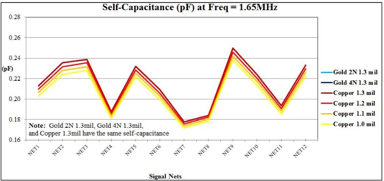
Just like that of the inductance, parasitic capacitance is also not dependent on
the conductivity of the material. Hence, signa nets with 1.3 mil wirebond diameter in Fig. 11 have the same self-capacitance regardless of the wirebond material.
Self-capacitance of a signal net is the total equivalent self-capacitance of the lead and wirebonds connected to it. Capacitance value increases as the area of the conductor increases, as depicted in Eq. (3). Copper 1.0 mil
has the lowest parasitic capacitance
performance among all wires.
performance of Device Z with different wirebond
configuration. Among the three electrical
properties, resistance has the most significant effect.The effect on self-capacitance is not
significant although results showed that
decreasing wirebond diameter decreases the self-capacitance. To minimize the electrical loss and to have better electrical performance, parasitic RLC should be minimized. With the
results, Copper 1.3 mil configuration has the best electrical performance.
4.2 Wirebond Cost Analysis
Analysis was done to compare the cost impact of using Copper wires versus the Gold wires. Table 3 shows the cost per unit for different wirebond material.
Fig. 9. Resistance comparison of signal nets with different wires
Fig. 11. Capacitance comparison of signal nets with different wires
Table 3. Wirebond cost per unit
Wirebond material Cost per unit 1,2 (In comparison with Gold 4N)
Gold 4N 1.3 mil 100.00% – Reference
Gold 2N 1.3 mil ~100.00%
Copper 1.3 mil (CuPd) 6.00%
Copper 1.2 mil (CuPd) 6.00%
Copper 1.2 mil (Bare Cu) 2.32%
Copper 1.0 mil (Bare Cu) 1.85%
1
Cost per unit in $ intentionally not given; 2 For total wirebond length of 24.631 mm
With Gold 4N 1.3 mil as the price reference, the cost of using CuPd (Copper wire coated with Palladium) 1.3 mil is just 6% of the cost of the Gold wire. For the bare Copper 1.0 mil, only 1.85% of the total Gold wire cost. Clearly, Copper wire technology offers massive cost savings and could pave way for more businesses in the plant.
5. CONCLUSIONS AND
RECOMMENDA-TION
A comprehensive study of package electrical modeling and simulation was showcased for Device Z with different wirebond configurations: Gold 2N 1.3 mil, Gold 4N 1.3 mil, Copper 1.3 mil, Copper 1.2 mil, Copper 1.1 mil and Copper 1.0 mil. The models were analyzed at DC and AC for the RLC extraction.
Among the three electrical properties, resistance has the most significant effect. The effect on self-capacitance is not significant although results show that decreasing wirebond size decreases the self-capacitance value. To minimize the electrical loss and to have better electrical
performance, RLC should be minimized. As explained and shown in the results, Copper 1.3
mil wirebond configuration has the best electrical performance in terms of minimizing
RLC.
Based on the technical data from one of the wirebond suppliers [11], Gold 4N 1.3 mil and Copper 1.1 mil have the closest (and the same) fusing currents with 0.85 A. Although Gold 4N 1.3 mil has slightly lower resistance values than Copper 1.1 mil, still their results are comparable and not significantly different. Prioritizing the wirebond thickness without sacrificing the electrical performance, Copper 1.1 mil would be the best replacement for Gold 4N 1.3 mil wirebond configuration. However, since Copper 1.1 mil is not yet available in the market, Copper 1.2 mil could be used, with better electrical parameters.
Cu) is just 1.85% of the total cost of the Gold 4N 1.3 mil reference – that is 98.15% cost savings. Ultimately, Copper wire technology offers massive cost savings and could pave the way for more businesses in the plant.
For future works, Silver (Ag) wires and Silver-alloy wires could be explored and studied for package modeling, cost analysis, and for manufacturability.
ACKNOWLEDGEMENT
The authors would like to express
sincere gratitude to the New Product
Development & Introduction (NPD-I) team and colleagues of STMicroelectronics Calamba
who have greatly contributed to the success
of the work. The authors are thankful to the Management Team for the countless
support.
COMPETING INTERESTS
Authors have declared that no competing interests exist. The products used for this research are commonly and predominantly use products in our area of research and country. There is absolutely no conflict of interest between the authors and producers of the products because we do not intend to use these products as an avenue for any litigation but for the advancement of knowledge. Also, the research was not funded by the producing company rather it was funded by personal efforts of the authors.
REFERENCES
1. Liu Y, Irving S, Luk T, Kinzer D. Trends of power electronic packaging and modeling. 10th Electronics Packaging Technology Conference, Singapore; 2008.
2. Tsukada Y, Kobayashi K, Nishimura H.
Trend of semiconductor packaging, high density and low cost. 4th International Symposium on Electronic Materials And Packaging, Taiwan; 2002.
3. Chauhan PS, Choubey A, Zhong ZW,
Pecht MG. Copper wire bonding. 1st ed., New York, USA: Springer-Verlag; 2013. 4. Tan CE, Liong JY, Dimatira J, Tan J, Kok
LW. Challenges of ultimate ultra-fine pitch process with gold wire & copper wire in qfn packages. 36th International Electronics Manufacturing Technology Conference, Malaysia; 2014.
5. Bowick C. RF circuit design. 1st ed., Howard W. Sams & Co. Inc., Indianapolis, Indiana, USA; 1982.
6. May GS, Spanos CJ. Fundamentals of
semiconductor manufacturing and process control, 1st ed., Wiley-IEEE Press, USA; 2006.
7. Heraeus Electronics, Bonding Wires for
Semiconductor Technology.
Available:https://www.heraeus.com/media/ media/het/doc_het/products_and_ solutions_het_documents/bonding_wires_ documents/Brochure_Bonding _Wire.pdf
8. ANSYS Inc., ANSYS Electronics Desktop.
Available:https://www.ansys.com/products/ electronics/ansys-electronics-desktop
9. Autodesk, Inc., AutoCAD.
Available:https://www.autodesk.com/produ cts/autocad/overview
10. SAS Institute Inc., JMP Statistical
Discovery Software.
Available:https://www.jmp.com/en_ph/soft ware.html
11. TANAKA electronics. Physical and
electrical properties for Au, CuPd wire and Bare Cu wire.
Available:https://pro.tanaka.co.jp/en/produ cts/Bonding_Wires.html
© 2019 Gomez et al.; This is an Open Access article distributed under the terms of the Creative Commons Attribution License (http://creativecommons.org/licenses/by/4.0), which permits unrestricted use, distribution, and reproduction in any medium, provided the original work is properly cited.
Peer-review history: