DEVICES AND FILMS
by Kasandra Wolf
A thesis
submitted in partial fulfillment of the requirements for the degree of Master of Science in Electrical Engineering
Boise State University
DEFENSE COMMITTEE AND FINAL READING APPROVALS
of the thesis submitted by
Kasandra Wolf
Thesis Title: Radiation-Induced Effects in Chalcogenide-Based Memory Devices and Films
Date of Final Oral Examination: 10 July 2014
The following individuals read and discussed the thesis submitted by student Kasandra Wolf, and they evaluated her presentation and response to questions during the final oral examination. They found that the student passed the final oral examination.
Maria I. Mitkova, Ph.D. Chair, Supervisory Committee William B. Knowlton, Ph.D. Member, Supervisory Committee Dmitri Tenne, Ph.D Member, Supervisory Committee
iv DEDICATION
v
ACKNOWLEDGEMENTS
I would like to express my sincere gratitude to my advisor Dr. Maria Mitkova for her continued encouragement, guidance, and enthusiasm throughout my collegiate career. I am grateful for the opportunities provided to me by her as well as the advice she
imparted to me. Working for and learning from her was a true pleasure.
I would like to thank my committee members Dr. Bill Knowlton and Dr. Dmitri Tenne for advising and sharing their knowledge with me. I am thankful to Dr. Tenne in particular for his patience and helping me learn about Raman spectroscopy. Also, I would like to express my gratitude to Dr. Michael Kozicki and Dr. Hugh Barnaby who were co-Primary Investigators on the project for providing valuable discussions regarding the experimental procedures and assisting in the interpretation of results.
Additionally, I’m thankful to Pete Miranda, the Director of Idaho
Microfabrication Laboratory, for training me on the equipment and his assistance in obtaining quality results. I would like to acknowledge Dr. Karthik Chinnathambi for assisting with measurements on the XRD.
vi
collaborators at Arizona State University, Dr. Yago Gonzalez-Velo, Jennifer Taggart, and Herbert Bowler.
A special thank you goes to the sources of financial support: the Department of Defense – Defense Threat Reduction Agency (DOD-DTRA) and the Department of Energy-Nuclear Engineering in University Program (DOE-NEUP). Thank you to the faculty and staff of the Boise State University Department of Electrical and Computer Engineering and Donna Welch for everything they have done to help me.
Finally, I am grateful to my family and friends for their love and continued support. Thank you to my mom and dad for providing unwavering support as I pursued my collegiate studies. Thank you to my sister and brother for their love and
vii ABSTRACT
Continued scaling of memory devices has produced many issues for the current foremost non-volatile memory—the flash memory—leading to the emergence of a wide variety of alternative memory solutions. Redox Conductive Bridge Memory (RCBM) is one such solution that has shown great promise in recent years. However, the
performance of these devices under radiation conditions has not been explored in detail. This work investigates the effects of x-rays and electron bombardment on chalcogenide glasses and RCBM devices based on these materials.
RCBM devices are a form of Resistance Change Memory, which rely on two distinct resistive states to represent the binary ‘0’ and ‘1’ memory conditions. The functionality of the RCBM devices is based on the growth and dissolution of a conductive filament through an insulating medium sandwiched between two metal electrodes. The presence of the filament represents the on state, while the absence represents the off state.
viii
of the effects occurring in the systems comprising the RCBM devices. The major
ix
TABLE OF CONTENTS
DEDICATION ... iv
ACKNOWLEDGEMENTS ... v
ABSTRACT ... vii
LIST OF TABLES ... xiii
LIST OF FIGURES ... xiv
LIST OF ABBREVIATIONS ... xix
CHAPTER 1: IONIZING RADIATION ... 1
Forms of Ionizing Radiation ... 1
Generation of X-Rays ... 2
Formation of Electron Beams ... 9
Interaction of Ionizing Radiation with Matter ... 10
Electromagnetic Radiation ... 11
Electron Beam Radiation ... 13
CHAPTER 2: CHALCOGENIDE GLASSES ... 17
Material Classifications ... 17
Glass Preparation ... 18
Chalcogenide Glasses ... 19
x
CHAPTER 3: RADIATION-INDUCED EFFECTS IN CHALCOGENIDE GLASSES ... 25
Electromagnetic Radiation ... 25
Absorption Edge ... 25
Sub-Bandgap Photons ... 26
High Energy Photons ... 29
Electron Beam Radiation ... 32
CHAPTER 4: Ag-CONTAINING CHALCOGENIDE GLASSES AND MEMORY APPLICATIONS ... 35
Mechanisms of Ag Diffusion into Chalcogenide Glass ... 35
Ag Diffusion ... 35
Ag Diffusion with External Forces ... 37
Structures of Ag-Doped Chalcogenide Glass ... 38
Basics of Resistance Change Memory ... 39
Ferroelectric Memory ... 40
Phase-Change Memory ... 41
Redox Conductive Bridge Memory ... 42
Switching Mechanisms in RCBM ... 42
Reduction-Oxidation Mechanisms in RCBM ... 43
CHAPTER 5: EXPERIMENTAL PROCEDURE ... 46
Film Fabrication ... 47
Amorphous GexSe100-x Films ... 47
Ag Source Formation ... 48
RCBM Device Fabrication ... 49
xi
Sputtering of W and Field Isolation SiO2 ... 51
Photolithography ... 51
Wet Etching of SiO2... 53
Thermal Evaporation of Ge-Se Active Layer ... 53
Ag Pad and W Pad Formation ... 54
Film Characterization Methods... 54
Raman Spectroscopy ... 54
Energy Dispersive Spectroscopy (EDS) ... 55
X-ray Diffraction (XRD) ... 56
Device Characterization Method ... 57
CHAPTER 6: INFLUENCE OF SUB-BANDGAP LIGHT ON CHALCOGENIDE GLASS ... 58
Radiation Exposure Conditions ... 58
Results ... 59
Discussion ... 63
Conclusion ... 64
CHAPTER 7: X-RAY INDUCED EFFECTS IN THIN Ge-Se FILMS AND RCBM DEVICES ... 66
Radiation Exposure Conditions ... 66
Film Characterization... 67
RCBM Device Performance ... 71
Discussion ... 78
xii
CHAPTER 8: ELECTRON BEAM INDUCED EFFECTS IN THIN Ge-Se FILMS
AND RCBM DEVICES ... 82
Radiation Exposure Conditions ... 82
Film Characterization... 83
RCBM Device Performance ... 91
Discussion ... 96
Conclusion ... 98
FINAL REMARKS AND FUTURE WORK ... 99
Final Remarks ... 99
Future Work ... 101
xiii
LIST OF TABLES
Table 1. Chemical reactions occurring at the interface of Ag
xiv
LIST OF FIGURES
Figure 1. Schematic diagram representing the x-ray tube where x-rays are
produced by the Bremsstrahlung process ... 4 Figure 2. Spectra of Bremsstrahlung x-rays with various electron exciting
potential gradients [3] ... 5 Figure 3. Characteristic x-rays Kα and Kβ as produced by K shell emissions
from a molybdenum target [3] ... 6 Figure 4. Schematic diagram outlining major components of a modern synchrotron
source [6] ... 8 Figure 5. Electromagnetic spectrum describing the wavelengths and corresponding
photon frequencies. Reprinted with permission from [8]
© 2012 Elsevier. ... 12 Figure 6. Generalized illustration representing products of electron bombardment;
secondary electrons and Auger electrons remain near the surface while backscattered electrons and characteristic x-rays exit the sample ... 14 Figure 7. Evolution of material viscosity during glass preparation process Ge-Se
Chalcogenide Glasses; the graph shows glass transition temperature (Tg),
melting temperature (Tm), and quenching temperature (TQ) ... 18
Figure 8. Glass transition temperature for (a) AsxS1-x (b) GexS1-x, and GexSe1-x.
(a) Reprinted with permission from [15] © 1966 the Japan Society of Applied Physics (b) Reprinted with permission from [16]
© 1997 the American Physical Society ... 20 Figure 9. Glass forming regions of binary chalcogenides; Se glasses have the largest
glass forming region. Reprinted with permission from [11]
© 2011 Springer and Springer eBook ... 20 Figure 10. Basic GeSe4 tetrahedron unit; Ge atom at the center of four equidistant
Se atoms ... 22 Figure 11. sp3 hybridization of Ge valence shell; all four electrons have the same
xv
Figure 12. Corner-sharing bond tetrahedral structure ... 24
Figure 13. Edge-sharing bond tetrahedral structure ... 24
Figure 14. Ethane-like Ge-Ge bonding structure ... 24
Figure 15. Distorted rock salt layered structure ... 24
Figure 16. Layered Rock Salt structure [25] ... 24
Figure 17. Absorption spectra of amorphous As-Se and Ge-Se; the glasses do not have a straight absorption edge which is centered around 550 nm. Reprinted from with permission from [26] © 2008 Elsevier. ... 26
Figure 18. Time evolution of transparency in GeSe2 film with switching light source; photodarkening (decreasing T/To) occurs in initial 110 secs; after 120 secs photobleaching (increasing T/To) starts Reprinted with permission from [38] © 2011 Elsevier ... 27
Figure 19. Possible structural changes in a-As2S3 with As-○ and S-● Reprinted with permission from [47] © 2004 Elsevier and Elsevier Books ... 31
Figure 20. Interaction of negatively charged sites through a double layered model of the glass network (a) electrons accumulate at sites in the network (b) negatively charged sites repel each other creating voids within the network Reprinted with permission from [50] © 2002 AIP Publishing LLC. ... 34
Figure 21. Comparison of photodiffusion and thermal diffusion of Ag in Ge20Se80 glass; saturation of Ag occurs faster with photo diffusion and also introduces more Ag into the glass than thermal diffusion Reprinted with permission from [63] © 2004 Elsevier ... 37
Figure 22. FeRAM cell design includes 1 access CMOS transistor and 1 ferroelectric capacitor Reprinted with permission from [66] © 1988 IEEE ... 41
Figure 23. Basic design of RCBM device with conductive bridge in place; the device shown is in the ON-state or LRS; a forward bias is being applied ... 42
Figure 24. Bipolar resistive switching in RCBM: (1) a negative bias is applied and the device remains in the OFF-state; (2) as the bias increases positively, it eventually reaches VTh; (3) device switches to ON-state and the current is limited by CC; (4) as the bias approaches 0, an ohmic relationship occurs; (5) when the negative bias reaches VEr, the device switches off [68] ... 43
xvi
Figure 26. Design of semi-Knudsen cell crucible used for thermal evaporation of amorphous GexSe100-x films; the mesh pattern of the cover equalizes
the partial pressures of Ge and Se in order to achieve ideal film
compositions ... 47 Figure 27. Shadow mask utilized in formation of thermally deposited Ag sources;
white dots were sealed so only a single row of Ag dots were deposited (shown in green) ... 48 Figure 28. Process flow for W/a-GexSe100-x/Ag RCBM devices... 50
Figure 29. Photolithography process developed for RCBM devices using SPR 220 photoresist ... 52 Figure 30. Time evolution of Ge29.2Se70.8 film transparency showing transient
photobleaching (increased T/To during pumping cycles and returning to original state during rest cycles) ... 59 Figure 31. Time evolution of Ge32.1Se67.9, and Ge39.5Se60.5 film transparency showing
transient photodarkening (decreased transparency) and metastable
photobleaching (permanently increased transparency) ... 60 Figure 32. Raman spectra of films before and after light exposure: a) Ge29.2Se70.8,
b) Ge32.1Se67.9, c) Ge39.5Se60.5 ... 61
Figure 33. Structural changes observed from Raman spectra: a) ratio of ES areal intensity to CS areal intensity, b) areal intensity of Se-Se chains, and c) areal intensity of ETH structures ... 62 Figure 34. Experimental setup of x-ray irradiation ... 66 Figure 35. Raman spectra of x-ray control and highest dose (60 krad) exposed films
for a) Ge22.6Se77.4, b) Ge32.4Se67.6, and c) Ge44.4Se55.6... 68
Figure 36. Areas of Gaussian curves fitted to Raman spectra: a) ratio of areas of ES curves to areas of CS curves, b) Areas of Se-Se band curves,
and c) Areas of ETH band curves ... 69 Figure 37. XRD patterns of films with Ag source exposed to x-rays show
development of β-Ag2Se a) Ge25.6Se74.4, b) Ge36.2Se63.8,
and c) Ge44.3Se55.7 ... 70
Figure 38. Distribution of write/erase voltages (green) and on/off-state resistances (red) for GexSe100-x (x=24.8, 36.2, and 44.3) RCBM devices exposed
xvii
Figure 39. Median memory windows for RCBM devices exposed to x-rays ... 74
Figure 40. Endurance testing data for 105 cycles on Ge24.8Se75.2 RCBM devices exposed to 0, 12 krad, and 24 krad of x-rays ... 75
Figure 41. Endurance testing data for 105 cycles on Ge36.2Se63.8 RCBM devices exposed to 0, 12 krad, and 24 krad of x-rays ... 76
Figure 42. Endurance testing data for 105 cycles on Ge44.3Se55.7 RCBM devices exposed to 0, 12 krad, and 24 krad of x-rays ... 77
Figure 43. Conversion of ES to CS structures within the Ge-Se network Reprinted with permission from[86] © 2011 American Chemical Society ... 78
Figure 44. Packing fraction of GexSe100-x ... 79
Figure 45. Electron beam radiation system ... 82
Figure 46. Deconvoluted Raman spectra of a) Ge22.6Se77.4, b) Ge26.1Se73.9, and c) Ge42.2Se57.8exposed to 0 and 1.05x10¹² rad of e-beam radiation ... 83
Figure 47. Area ratio of ES/CS from deconvoluted Raman spectra ... 84
Figure 48. Area of ETH from deconvoluted Raman spectra ... 84
Figure 49. Area of Se-Se curve from deconvoluted Raman spectra ... 84
Figure 50. Lateral diffusion of Ag as determined through EDS mapping ... 86
Figure 51. EDS mapping of Ag diffusion in a-Ge25.6Se74.4 a) Control, b) 6.3x10¹¹ rad, and c) 10.5x10¹¹ rad ... 86
Figure 52. EDS mapping of Ag diffusion in a-Ge36.2Se63.8 a) Control, b) 6.3x10¹¹ rad, and c) 10.5x10¹¹ rad ... 87
Figure 53. EDS mapping of Ag diffusion in a-Ge44.3Se55.7 a) Control, b) 6.3x10¹¹ rad, and c) 10.5x10¹¹ rad ... 87
Figure 54. XRD pattern of e-beam radiated Ge25.6Se74.4 with Ag source... 88
Figure 55. XRD pattern of e-beam radiated Ge36.2Se63.8 with Ag Source ... 88
Figure 56. XRD pattern of e-beam radiated Ge44.3Se55.7 with Ag source... 89
xviii
Figure 58. Grain growth of ternary Ag8GeSe6 phase in three different compositions 90
Figure 59. Grain growth in phase separated Ag in Ge44.3Se56.7 ... 90
Figure 60. Distribution of write/erase voltages (green) and on/off-state resistances (red) for GexSe100-x (x=24.8, 36.2, and 44.3) RCBM devices exposed
to 0, 2.1x10¹¹, and 4.2x10¹¹ rad of electron beam radiation ... 92 Figure 61. Endurance testing on Ge24.8Se75.2 RCBM devices exposed to 0 rad,
2.1x10¹¹ rad, and 4.2x10¹¹ rad of e-beam radiation ... 93 Figure 62. Endurance testing on Ge36.2Se63.8 RCBM devices exposed to 0 rad,
2.1x10¹¹ rad, and 4.2x10¹¹ rad of e-beam radiation ... 94 Figure 63. Endurance testing on Ge36.2Se63.8 RCBM devices exposed to 0 rad,
xix
LIST OF ABBREVIATIONS
ChG Chalcogenide Glasses
RCM Resistance Change Memory
RCBM Redox Conductive Bridge Memory
MIM Metal Insulator Metal
LRS Low Resistive State/On-State Resistance HRS High Resistive State/Off-State Resistance SEM Scanning Electron Microscope
XRD X-ray Diffraction
EDS Energy Dispersive Spectroscopy
BOE Buffered Oxide Etch
CHAPTER 1: IONIZING RADIATION
The increased need for scaling of memory devices has led to the emergence of alternative memory solutions. In many circumstances, these memory devices may be required to perform in extreme environmental conditions, for which performance data has not been disseminated. An example of such a circumstance is the application of these devices in space exploration. This work investigates the influence of radiation by x-rays and electron beam on the Redox Conductive Bridge Memory (RCBM) devices.
Forms of Ionizing Radiation
There are many types of radiation, of which there are two primary categories: ionizing and nonionizing radiation. Ionizing radiation is classified as any form of
radiation energy composed of photons or particles with enough kinetic energy to remove an electron from the valence band of an atom. The energy typically required to remove an electron from an atom is 4-25 eV [1].
neutrons, which transfer their energy to charged particles in the material upon which it is incident. The photoelectric effect occurs when an incident photon interacts with an electron and transfers all of its energy to the electron. If the photon transfers sufficient energy to the electron to release the electron from the bonding site, then this interaction results in the ionization of the atom. Depending on the amount of energy transferred, the excited electron can interact with other atoms and excite another electron deeper within the material.
Certain types of electromagnetic radiation are classified as indirectly ionizing radiation, including γ-rays, x-rays, ultraviolet light, and visible light for some materials. An ionizing photon with energy of 4 eV would have a corresponding wavelength of 300 nm. Conversion between the photon frequency and the photon energy was theorized by Max Plank [2]. This relationship between the energy (E) of the particle and the
wavelength (λ) is described by the following equations, in which h is Planck’s constant (4.136 x 10¹⁵ eV·s ), c is the speed of light (2.998 x 10⁸ m/s ), and f is the frequency of the electromagnetic wave.
= ℎ (1)
= (2)
= ℎ (3)
Generation of X-Rays
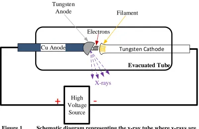
generated using three different methods: the Bremsstrahlung process, shell emission, or synchrotron radiation.
The Bremsstrahlung x-rays are generated when an electron passes through the electric field of a nucleus, causing the velocity of the electron to decrease. Due to the law of conservation of energy, the difference in energy from the electron entering and exiting the electric field is present in the form of a photon [3, 4]. This process is also known as the inverse photoelectric effect because kinetic energy from a moving electron is converted to an electromagnetic wave [3]. The wavelength of the resulting photon is described by the following equation, in which Ei is the energy of the electron as it is
entering the electric field and Ef is the energy as it exits.
=E − Eℎ (4)
Bremsstrahlung x-rays are produced using an apparatus similar to the diagram shown in Figure 1. Current passes through the heated filament (cathode) and emits
The Bremsstrahlung process produces x-rays in a wide spectrum of wavelengths; for this reason, Bremsstrahlung x-rays are also called an x-ray continuum, depicted in Figure 2. A single crystal target will produce a monochromatic and strongly collimated x-ray beam. However, by using a higher exciting potential, the relative range of
wavelengths can be highly minimized at the expense of having a broad tail in the spectrum. The effect of the tail can be significantly diminished by placing filters on the outside of the envelope.
Cu Anode
High Voltage
Source
+
-Tungsten Anode
Tungsten Cathode
Filament
X-rays
Evacuated Tube
Electrons
Figure 2. Spectra of Bremsstrahlung x-rays with various electron exciting potential gradients [3]
During the production of Bremsstrahlung x-rays, another event known as shell emission, which also produces x-rays, may occur. According to the Bohr model of an atom, electrons occupy orbits, or shells, at discrete distances from the nucleus. During shell emission, x-rays are generated when electrons in a higher energy shell transition to a lower energy shell [5]. The transition produces a photon with an energy equivalent to the difference in that of the shells [5]. The most common form of this event is Kα shell
emission, in which electrons transition into the innermost and lowest energy K shell from the adjacent L shell. X-rays produced from shell emission are known as characteristic rays since they have energies characterized by the atomic energy levels. Characteristic x-rays are denominated by the shell in which the electrons land in and a Greek letter (α, β,
γ, δ, etc.) that signifies the difference in the energy levels before and after the transition. For example, electrons that transition from the n=2 energy level to the n=1 energy level emit Kα x-rays, while electrons that transition from the n=3 energy level to the n=1
The apparatus for generating characteristic x-rays is similar to the apparatus for generating Bremsstrahlung x-rays. Electrons are ejected from the filament through thermionic emission and directed towards the anode, which holds the target. In this process, the incident electrons excite electrons from the K shell of the target atoms. Consequently, an electron from an outer shell of this atom transitions to a lower energy to fill the empty K shell; the difference in energy materializes in the form of a photon. The interaction between the incident electrons and the target atoms will produce both
Bremsstrahlung x-rays and characteristic x-rays. However, the relative intensities between the K shell emission x-rays and the Bremsstrahlung x-rays will be very large, thus ensuring that the output x-rays are primarily K shell emission x-rays. X-rays produced from the K shell emissions have a much higher intensity, higher wavelength and narrower range of wavelengths than the Bremsstrahlung x-rays [3]. An example of the K shell emission x-ray spectrum produced using a molybdenum target is shown in Figure 3.
Figure 3. Characteristic x-rays Kα and Kβ as produced by K shell emissions
A synchrotron source is a more sophisticated and modern method than the Bremsstrahlung tube and K shell emission for producing x-rays. With the aid of a synchrotron source, the most intense rays can be manufactured. In this method for x-ray generation, electrons are constantly accelerated radially around a large storage ring, illustrated in Figure 4, maintaining a nearly constant energy. In a modern synchrotron source, electrons are generated with a thermionic gun, and then accelerated using a linear particle accelerator (linac). The energized electrons are injected from the linac into the smaller ring, called the booster ring, as illustrated in Figure 4.
The electrons from the booster ring supply the larger storage ring. Once the synchrotron is in full operation, electrons from the booster ring are periodically injected into the storage ring in order to maintain the specified electron current [6]. Injection of electrons with energies other than the target energy into the storage ring causes strong disturbances in the electrons’ orbit and therefore interruptions of the experiments; consequently, the booster ring and storage rings are maintained at the same energies. Additionally, a constant electron current in the storage ring is maintained by frequently injecting electrons from the booster ring that ‘top-up’ the current when it drops below a small error window of approximately 1 mA [6].
The storage ring is actually a series of straightaways, containing insertion devices, and curves, which contain bending magnets to maintain a closed path. This ring supplies the electrons and/or radiation for any experiment and thus it is a crucial segment of the entire synchrotron operation. To ensure that the electron velocity is maintained
they approach the bending magnets and emit synchrotron radiation. This radiation is primarily x-rays generated through the Bremsstrahlung x-ray generation process. The difference between these x-rays and the Bremsstrahlung x-rays is the intensity and the ability to selectively determine the wavelengths, which is a function of the electron velocity and the strength of the bending magnets.
Figure 4. Schematic diagram outlining major components of a modern
synchrotron source [6]
Connected to the storage ring are beamlines, which are tangentially connected to the storage ring, situated at each bend of the storage ring. The beamline is composed of three major components: front end, optics, and the experimental hutch. The front end of the beamline serves several functions. It isolates the beamline vacuum from the storage ring vacuum, blocks x-rays, and Bremsstrahlung radiation (when necessary), selects the acceptable angular range radiation, and filters out the synchrotron radiation that is too low in energy [6]. The optics portion of the beamline serves to select the desired energies,
Bending
Magnets
Storage
Ring
RF
Insertion
Device
optics
experimental hutch
beamline
front end
focus the photons, and optimize the energy resolution of the beam [6]. Finally, the synchrotron x-rays reach the experimental hutch where the sample to be irradiated is located.
Formation of Electron Beams
Another type of radiation source is known as an electron beam. Electron beam (e-beam) technology is used in a wide variety of applications, including electron beam welding for industrial purposes, electron beam furnace for refining rare or refractory metals, electron beam lithography for producing semiconductor nanotechnology devices, and Scanning Electron Microscopy (SEM) and Transmission Electron Microscopy (TEM) for imaging microstructures.
The most crucial component for generating an electron beam is the electron gun. Two types of electron beam guns will be described here: thermionic emission and high field emission. The first form, the thermionic emission electron gun, is the most common form of electron gun used in SEM imaging. In the process of thermionic emission,
electrons escape the surface of the heated material by acquiring thermal energy. The most deterministic factor in this process is the work function of the heated material, which is the minimum amount of kinetic energy required for electrons to escape from the material. For an electron gun, the ideal work function would be very small in order to minimize the amount of energy required to generate electrons and maximize efficiency of the
equipment. Tungsten has a work function of 4.55 eV and is commonly used in electron guns. The maximum current density of the beam can be approximated using the
function (eV), k is Boltzmann’s constant (8.617 x 10⁻⁵ eV/K), and A is a material constant with an ideal value of 120 A/cm2 [6].
= (5)
High field emission is another method for generating electrons, most commonly used in the early forms of electron microscopy. Electrons are generated by the application of a strong electric field between two fine-point electrodes. Electrons escape the surface of the cathode through Fowler-Nordheim tunneling [7]. The current density at the point of the electrode is given by Equation (6), where E is the electric field intensity at the
emitter, Φ is the work function of the emitting material, and K is a constant
approximately equal to 1 [7]. The miniscule surface area of the emitter limits the amount of the electron current produced. The number of emitter sites can be increased and arranged into an array in order to increase the total amount of current produced. However, this type of arrangement may lead to a non-Gaussian distribution in the electron beam.
Interaction of Ionizing Radiation with Matter
Whether the form of ionizing radiation is directly or indirectly ionizing, it will react with solid materials in the same manner: displacement of an electron from the atom. The difference arises in the manner in which the radiation source interacts with the material to create an ionized atom. Directly ionizing radiation and indirectly ionizing radiation interaction with material are described separately due to their unique properties and effects.
= 1.54 × 10 . !×"#$ % & ⁄
Electromagnetic Radiation
As mentioned previously, electromagnetic forms of ionizing radiation are indirectly ionizing because photons are uncharged particles that transfer energy to charged particles in the material. In turn, these newly energized charged particles ionize atoms in the material through Coulombic interactions. Depending on the wavelength, and subsequently the energy, electromagnetic radiation can affect solid materials differently. Most solid materials are transparent to larger wavelength radiation like microwaves, which have wavelengths between 1 mm and 1 meter and corresponding photon energies between 1.24 meV and 1.24 µeV. Thus, radiation with long wavelength (i.e. λ > 10-3 m) and concurrently low photon energy passes through most solid materials without losing energy or affecting the materials.
Figure 5. Electromagnetic spectrum describing the wavelengths and corresponding photon frequencies.
Reprinted with permission from [8] © 2012 Elsevier.
When a photon is incident upon an atom, an electron of that atom may absorb all of the photon’s energy. If the amount of energy absorbed is greater than the binding energy of the electron, then the electron will have enough energy to escape the atom, effectively ionizing the atom. Most commonly this will occur with an electron from the valence shell. Since this electron was part of a bond with another atom, after excitation from this state, the bond is now broken. The photoelectric effect is the observation of an ejected electron after absorbing all of a photon’s energy [3, 5]. The photoelectric effect is most commonly observed with visible light incident on metallic materials, which have low ionization energies [3]; however, it can also be observed in semiconductor materials when higher energy photons are used (e.g., x-rays).
transferred to a stationary electron, which is then ejected from the location after the interaction with light [5]. The interaction of the photon with the electron results in the formation of an energetic electron and a remnant photon. Due to the law of conservation of energy, the resultant photon energy must equal the difference between the incident photon energy and the kinetic energy of the ejected electron. After the inelastic collision, the resulting photon will have less energy and a longer wavelength. If the resultant photon has enough energy, it may ionize a secondary atom through the photoelectric effect. Otherwise, the remnant photon is absorbed by another electron, exciting the electron to a higher energy level.
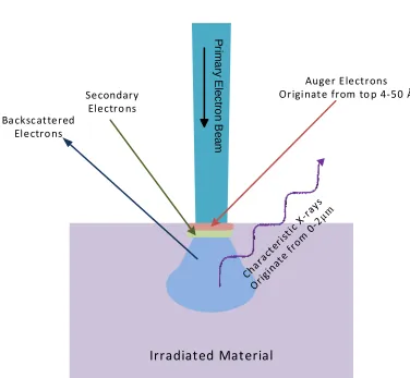
Electron Beam Radiation
Electron beam radiation is a form of directly ionizing radiation. Interaction between an electron beam and a solid material can cause a wide range of events, depicted in Figure 6, including the following: generation of backscattered electrons; generation of secondary electrons; electron hole pair recombination; electron transmission; and
Bremsstrahlung and characteristic x-ray generation. The energy of the incident electrons will determine which events transpire. In most cases, multiple different forms of events will occur.
A backscattered electron is a consequence of an elastic interaction, meaning no energy is transferred, between a beam electron and the nucleus of the specimen. In this interaction, the electron is scattered back out of the surface of the specimen. The electron is attracted to the nucleus of the atom by the Coulomb force, as described by
Equation (7), in which e is the elementary charge, Q2 is the charge of the nucleus, and r is
P
rim
a
ry
E
le
c
tro
n
B
e
a
m
Ba cksc at tered Electro ns
Secondary Electro ns
Auger E lectrons Origi nat e from to p 4-50 Å
Irradiated Material
Figure 6. Generalized illustration representing products of electron bombardment; secondary electrons and Auger electrons remain near the surface
while backscattered electrons and characteristic x-rays exit the sample
+ =− ,4-. (7)
The equation for Coulomb force reveals that the force is stronger for atoms with higher atomic number Z. Therefore, atoms with higher Z will generate more
backscattered electrons than atoms with lower Z, due to the relative number of protons in the nuclei. In scanning electron microscopes, backscattered electrons can be used to detect different compositions, grain boundaries, and phase boundaries.
incident electron will transfer kinetic energy to the bounded electron, providing enough energy for this electron to escape the valence shell of the atom.
Electron hole pair recombination within the material can result in numerous outcomes including characteristic x-rays, Auger electrons, and cathodoluminescence. Characteristic x-rays, as described previously, emerge when an electron from an outer shell falls into an empty shell closer to the nucleus. The difference in energy between the two shells manifests as an x-ray photon. Auger electrons are formed in a manner similar to characteristic x-rays with the exception that the energy from the electron is transferred to another electron in the outer shell [5, 9]. The excited electron is then ejected from the outer shell. The final product of electron hole pair recombination is cathodoluminescence and occurs in semiconductor materials. An interaction between a beam electron and an electron in the valence band of the semiconductor excite the electron into the conduction band, leaving behind a hole. This energetically unstable state leads to the electron hole pair recombination and the discharge of a photon with the difference in energy [9]. Cathodoluminescence only occurs in semiconductors because the energy bandgap is within the energy range of visible light.
CHAPTER 2: CHALCOGENIDE GLASSES
Chalcogen elements are those that compose Group VIA of the periodic table, most notably, sulfur (S), selenium (Se), and tellurium (Te). Materials that contain these elements are distinguished as chalcogenides. Chalcogenides have a wide range of uses, including applications in solar cells, memory storage, and inorganic photolithography. This chapter will detail chalcogenide glasses, a specific class of these materials, and their unique properties.
Material Classifications
Solid materials take one of three forms: crystalline, polycrystalline, or amorphous. Crystalline materials exhibit long range order where a unit cell is replicated and repeated periodically throughout the entire solid. In these types of materials, once the exact
location of an atom and its nearest neighbors are known, the placement of any other atom throughout the crystal can be predicted. Polycrystalline materials are composed of
multiple different crystallites or grains varying both in size and orientation. The third type of solid is amorphous material, e.g. fused silica (SiO2), which exhibit the greatest amount
Glass Preparation
Glasses compose a large segment of amorphous materials. The traditional method of glass formation involves melting the materials from pebble or powder form, then cooling the material at a rapid quench rate [10]. The glass synthesis process is summarized in a graph in Figure 7, with further details to follow.
Figure 7. Evolution of material viscosity during glass preparation process Ge-Se Chalcogenide Glasses; the graph shows glass transition temperature (Tg), melting
temperature (Tm), and quenching temperature (TQ)
Initially, the raw materials in pebble form are precisely measured in order to achieve the exact ratio of elements. These materials are vacuum sealed into a fused silica ampoule to avoid oxygen and other contaminants. The sealed ampoule is placed into a specialized rocking furnace, which slowly increases the temperature to the melting temperature (Tm), described as Step 1 in Figure 7. Once the melt reaches Tm, it
experiences a dramatic change in viscosity (Step 2). At this point of the synthesis, the furnace, with the ampoule, is rocked to ensure uniform mixture of all elements
throughout the melt. Heating and mixing of the melt continues (Step 3) until it reaches a specified quenching temperature (TQ), at which point it is cooled (Step 4). If the melt is
V
is
c
o
s
it
y ΔV
Temp erature
1
2 3
4
5
Tm
allowed to cool slowly, indicated by the dotted line in Figure 7, the material structure will transform towards the lowest entropy state, which is crystalline. The temperature at which the glass transitions from a solid to a supercooled liquid is known as the glass transition temperature (Tg). To maintain the amorphous nature of the melt in the
solidified material, the ampoule is swiftly removed from the furnace and quenched in air, water, or an ice bath, which forces the material to quickly surpass Tg, preventing
crystallization and maintaining a high viscosity (Step 5). Depending on the required quench rate, the quench time can range between milliseconds and hours [11]. Glasses can be created using any system of elements with variable stability, but in different systems there are only certain compositions, known as glass forming regions, in which stable glasses can be formed.
Chalcogenide Glasses
Chalcogenide glasses are covalently bonded glasses that contain at least one of the chalcogen elements. In chalcogenide glasses, the chalcogen elements can be combined with other elements for various applications. For instance, GeSe4 has demonstrated
applicability in NO2 gas sensors [12, 13]; GeSbTe has been used widely in rewritable
optical discs as a form of phase-change memory [14]. This study will focus on Ge-Se glasses due to properties that are favorable for resistive-memory devices in harsh radiation environments.
only three-fold coordinated. For example, the transition temperature of As30S70 is 100 °C
while that of Ge30S70 is 400 °C, as determined from the data in Figure 8a and b.
Figure 8. Glass transition temperature for (a) AsxS1-x (b) GexS1-x, and GexSe1-x.
(a) Reprinted with permission from [15] © 1966 the Japan Society of Applied Physics (b) Reprinted with permission from [16] © 1997 the American Physical
Society
Figure 9. Glass forming regions of binary chalcogenides; Se glasses have the largest glass forming region. Reprinted with permission from [11] © 2011 Springer
The pairing of the different chalcogen atoms (S, Se, or Te) with germanium, forming the binary Ge-chalcogen glass system, offers distinct properties. Sulfur and selenium containing glasses have similar properties that are ideal for certain types of resistive memory devices. However, selenium containing glasses have some advantages over sulfur containing glasses in radiation environments. Firstly, Ge-Se systems have a larger glass forming region than Ge-S systems, as displayed in Figure 9 [11]. The smaller glass forming region in Ge-S glasses is attributed to the phase separation of sulfur, which easily occurs in sulfur containing glasses. In the case of phase separation, rings of eight sulfur atoms with bond angles of 105° form, which become completely disconnected from the rest of the glass network [17]. Comparatively, selenium containing glasses form hexagonal chains, which run parallel to each other and have bond angles of 103.1° [18]. The bonding forces between the chains are van der Waals forces, which makes these glasses much more flexible; therefore, phase separation is less likely to occur [18]. Additionally, Ge-Se bonds have a longer bonding length (2.135 Å) and smaller bonding energy (485 kJ/mol) than those of Ge-S bonds (2.012 Å, 534 kJ/mol) [19].
The significantly weaker bonds and narrow bandgap common in telluride glasses cause dissimilar electrical and optical performances when compared to the other two chalcogen systems [20, 21]. Additionally, telluride glasses have a small glass forming region, shown in Figure 9, which limits the flexibility to study different compositions offering unique structures that are easily achievable in the other chalcogen systems. Elemental Te cannot form a glass, but Te containing glasses have the lowest Tg of the
the Tg of Ge20Te80 at 147 °C [23, 24]. For applications in harsh radiation environments,
glasses with higher Tg materials are desirable in order to avoid crystallization.
Structural Units of Ge-Se Glass
Since the structure of the disordered materials is of major importance for their performance and is studied in detail in this work, the fundamentals of the structure of the Ge-Se glasses are presented here. They consist of a basic unit cell: a GeSe4 tetrahedron,
shown in Figure 10. It contains a single Ge atom at the center surrounded by four covalently bonded Se atoms, each at a bond angle of 109.5°.
Figure 10. Basic GeSe4 tetrahedron unit; Ge atom at the center of four
equidistant Se atoms
The formation of the tetrahedron is due to the sp3 hybridization of the Ge atom. According to the valence bond theory, the ground state electron configuration of Ge is [Ar] 3d104s24p2 with the 4s2 orbital full and the two 4p2 electrons ready to react with their neighbors, as depicted in the left side of Figure 11. However, since the 4s and 4p energy levels are quite close, when Ge comes in contact with other atoms, interaction results in the four orbitals ψ(3s), ψ(3px), ψ(3py), and ψ(3pz), mixing together to form four new
hybrid orbitals. Because the same amount of energy is required to remove each electron from the valence shell of Ge, there cannot be two different energy levels. Thus, the hybrid orbital is formed at energy lower than the 4p orbital and higher than the 4s orbital.
Se Ge
Se Se
This orbital is called the sp3 hybridized orbital because it is formed from one s orbital and three p orbitals. The sp3 hybridized orbital is the reason that Ge is typically observed in a tetrahedral structure.
Figure 11. sp3 hybridization of Ge valence shell; all four electrons have the same energy
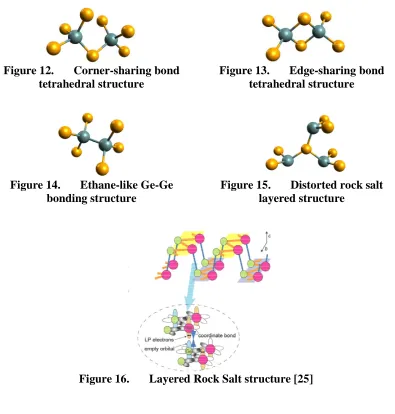
Amorphous Ge-chalcogenide materials are composed of several basic structural units: corner-sharing tetrahedral (CS) structures, edge-sharing tetrahedral (ES) structures, ethane-like structures of Ge-Ge bonds (ETH), chalcogen chains (Se-Se or S-S), and distorted rock salt structures [25].
There are two structural units that are each composed of two unit cell tetrahedra: corner-sharing and edge-sharing tetrahedral structures. The corner-sharing tetrahedral structure, shown in Figure 12, consists of two unit cell tetrahedra that share one chalcogen atom, which is situated at the corner of both unit cells. The bonds that the corner Se atom shares with two Ge atoms fill the valence shell of the Se atom and satisfy the 8-N rule [3]. This structure contains a 2:7 ratio of Ge:Se atoms. The edge-sharing tetrahedral structure, shown in Figure 13, consists of two unit cell tetrahedra that share two Se atoms to form an edge in the structure. In the edge-sharing, structure there is a 2:6 ratio of Ge:Se atoms.
The ethane-like bonding structure, shown in Figure 14, consists of two Ge atoms, each Ge atom bonded with three different Se atoms. In this structure, the two Ge atoms
4p
4s
E
n
e
rg
y
sp3
are covalently bonded together, which fills the last sp3 hybrid orbital to satisfy the 8-N rule. Glasses containing high Ge content (i.e., ≥ 40%) will sometimes contain another structure in which both Ge and Se atoms are three-fold coordinated. This structure only occurs when there are insufficient Se atoms present to satisfy the 8-N requirement of a Ge atom. This Ge atom will form a dative bond with the lone pair electrons of a Se atom, thereby satisfying its valence shell.
Figure 12. Corner-sharing bond
tetrahedral structure
Figure 13. Edge-sharing bond
tetrahedral structure
Figure 14. Ethane-like Ge-Ge bonding structure
Figure 15. Distorted rock salt layered structure
CHAPTER 3: RADIATION-INDUCED EFFECTS IN CHALCOGENIDE GLASSES
The structural units of Ge-Se glasses were described in Chapter 2. The ways in which these structural units are connected together form the backbone of the glass and determine the flexibility of the glass network. This chapter will explore the effect of two different forms of radiation on Ge-Se glasses: electromagnetic and electron beam. As previously mentioned with respect to materials in general, these forms of radiation will interact with chalcogenide glasses in different manners due to the difference in nature of photons and charged particles. Electromagnetic radiation interaction with chalcogenide glasses will be divided into two different groups: (1) sub-bandgap photons and (2) high energy photons.
Electromagnetic Radiation
Absorption Edge
Ge-Se films ranges from 500 nm to 575 nm, which corresponds to photon energies ranging between 2.15 eV and 2.48 eV [26]. Chalcogenide glasses are highly transparent for wavelengths greater than 575 nm and highly applicable for fiber optic applications [27, 28]. Photons with energies greater than 2.48 eV are absorbed and affect the structural performance and properties of the Ge-Se glass, which makes these materials highly applicable for this research.
Figure 17. Absorption spectra of amorphous As-Se and Ge-Se; the glasses do not have a straight absorption edge which is centered around 550 nm.
Reprinted from with permission from [26] © 2008 Elsevier.
Sub-Bandgap Photons
Two prominent effects have been discovered as resulting from the interaction of visible and ultraviolet light with Ge-Se glasses. These two effects are known as
recordings, optomechanical transducers, etc. [29-33]. In some amorphous chalcogenide materials, such as a-GeSe materials, a dual role of both photobleaching and
photodarkening was observed [34-36]. However, over longer time periods, photobleaching is more dominant [37].
Figure 18. Time evolution of transparency in GeSe2 film with switching light
source; photodarkening (decreasing T/To) occurs in initial 110 secs; after 120 secs photobleaching (increasing T/To) starts
Reprinted with permission from [38] © 2011 Elsevier
Studies on Ge-As-chalcogenide glasses have demonstrated the coexistence of both photobleaching and photodarkening, where photodarkening will occur immediately with radiation exposure. After an initial period, photobleaching will become more dominant over photodarkening [35, 36]. The switching from photodarkening to photobleaching is evident in the inset graph of Figure 18. It is hypothesized that this transient photodarkening is due to the formation of intermediate states between the ground state and the photo-excited states energies of electrons [38]. This type of result is attributed to breaking bonds and subsequent molecular rearrangement. The destruction of bonds causes the rearrangement of traps within the bandgap of the material, thus
photodarkening, the first of which states that the broadening of the valence band changes the bandgap [39-45]. The other theory suggests that the extended intermediate states affect the change in the bandgap due to excited charge carriers [39-45]. These two theories are based on the formation of defects, which originate from the breakage of bonds. The specific defects that contribute to photodarkening are located within the bandgap of the material and act as localized states. Increasing the number of defects, the bandgap of the material reduces since there are an abundant number of defect sites in near proximity for an electron to hop from one defect to another.
The other dominating effect is photobleaching of the Ge-chalcogenide glasses, which is also attributed to two different mechanisms. The first mechanism is photo-oxidation of Ge near the surface of the film. Photobleaching due to photo-photo-oxidation has been studied by comparing the transmission spectra of GeSe2 and Ge2Se3 films in air and
vacuum [37]. The results of this study suggest that in Ge-rich films, 40 at. % Ge, photobleaching is dominated by the photo-oxidation mechanism [37]. In lower Ge-content films, photobleaching is dominated by the second mechanism, changes in the structural ordering [37]. The structural reordering is generalized as a conversion of homopolar bonding structures to heteropolar bonding structures. More specifically, the ethane-like structures, which contain a Ge-Ge bond, and the Se-Se chains reorganize to form structures with Ge-Se bonds (i.e., GeSe4 tetrahedra that can be connected by either a
corner or an edge) [36]. The bond conversion is described by chemical reaction in Equation (8) [36].
Photodarkening and photobleaching were observed under sub-bandgap light, but similar structural changes and defect formations have also been studied in chalcogenide glasses exposed to high energy photons.
High Energy Photons
Chalcogenide glasses exposed to high energy photons will experience the same effects as when exposed to sub-bandgap photons, in addition to changes associated solely to the high energy photons. The effects of high energy photons can be further categorized as dynamic and static changes in the structural network of the glass. Dynamic changes are those that will decay over a period of time after radiation exposure is stopped (e.g., electron-hole pair generation). In the case of dynamic changes, the structure may revert back to its original state (e.g., electron-hole pair recombination). On the other hand, static changes are those changes that remain after radiation exposure has ceased, such as bond breaking and molecular rearrangement.
Radiation-Induced Dynamic Effects
Electron-hole pair generation is a dynamic effect of photon radiation. In this event, an atom absorbs the energy of a photon. An electron within the atom becomes excited enough to exit the atom, leaving a hole in its place. A study on a-Se systems has demonstrated the dynamic electronic charge neutralization of defects in the network by electrons and holes generated during photon illumination [46]. Initially, the positively charged, over-coordinated Se atoms will trap electrons, while the holes will be trapped around the singly bonded, under-coordinated, and negatively charged Se atoms, effectively neutralizing the electric charge of these atoms [46]. Eventually, the
freely within the network without being trapped [46]. This study also observed that the decreasing amount of defects led to a shift in the Fermi level towards the valence band, which increased the conductivity of the p-type semiconductor [46]. It is believed that the observed effects are due to charge trapping rather than electron-hole pair recombination, because the charged defects revert to their original state after the termination of photon illumination [46].
Radiation-Induced Static Effects
The majority of the changes in the structural network of the glass are primarily related to the radiation-induced static changes. A broken bond resulting from the
absorption of a photon forces the surrounding network to rearrange in order to fulfill the 8-N rule for each atom. The details of which particular bond is formed are dependent upon the atoms involved in the broken bond as well as the possible defects situated adjacent to the broken bond. The amorphous nature of the network provides a wide range of possibilities in bond transformations, as illustrated in Figure 17 for the binary As-S system. One possibility, known as destruction-polymerization, is the destruction of a homopolar bond in favor of a heteropolar bond, as illustrated in No. 1-4 in Figure 19, or the destruction of a heteropolar bond in favor of a homopolar bond, No. 9-12. [47].
Figure 19. Possible structural changes in a-As2S3 with As-○ and S-●
Reprinted with permission from [47] © 2004 Elsevier and Elsevier Books
amorphous chalcogenide glasses and γ-rays as well as x-rays, due to the similar photon energies relative to the bonding energies within the glasses. Photon radiation-induced static effects must comply with the following principles [47]:
1. All statistically possible transformations must be considered, which can be described by a single generalized equation: broken bond → created bond Additionally, a single broken bond can only result in the formation of another single bond.
2. The interaction of high energy radiation with the amorphous network may result in the formation of weaker ‘wrong’ bonds over the stronger bonds. This transformation of a previously strong bond into a bond consisting of a lower bonding energy causes a low-energetic shift of the absorption edge leading to the decrease in the bandgap of the system.
3. High energy radiation with the amorphous network may result in the
formation of strong bonds over wrong bonds. The formation of strong bonds will lead to a high-energetic shift in the absorption edge and an increase in the bandgap of the system.
4. In a close packed glass network with high atomic density, only
transformations with high energy differences may occur. This rule does not apply to amorphous chalcogenide glasses with low density due to the abundance of voids within the network.
Electron Beam Radiation
typically greater than 1 keV, which is in the same energy range as x-rays and γ-rays. Therefore, some similarities are expected between the interactions of electron beam radiation with chalcogenide glass and the interactions of x-rays and γ-rays with chalcogenide glass.
The similarities between the effects on chalcogenide glass due to high energy electrons and high energy photons include electron-hole pair generation and static structural changes in the glass network. The primary difference between these two types of radiations is the type of particle that delivers the radiation. Photon particles may be completely absorbed by particles within the glass after interactions. On the other hand, electrons will remain within the glass after interactions with the material unless there is a conductive path that allows them to escape. The buildup of negative charges within the glass is called charging [48]. For this reason, specimens in scanning electron microscopes are grounded through the sample holder.
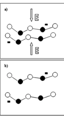
In electron beam radiation, high energy electrons travel into the chalcogenide glass and interact with the structure of the material. These incident electrons collect at localized sites within the glass [49]. The collection of newly introduced electrons creates a localized and negatively charged electric field [49, 50]. The different sites where electrons are collected interact with each other through electrostatic forces [49, 50]. One study models the network as a layered network to demonstrate the interaction of
negatively charged sites [50]. The negatively charged sites will experience repulsion and force the surrounding amorphous network to accommodate the electric fields, as
Figure 20. Interaction of negatively charged sites through a double layered model of the glass network (a) electrons accumulate at sites in the network (b) negatively charged sites repel each other creating voids within the network
Reprinted with permission from [50] © 2002 AIP Publishing LLC.
CHAPTER 4: Ag-CONTAINING CHALCOGENIDE GLASSES AND MEMORY APPLICATIONS
Up to this point, chalcogenide glasses as well as the effects of radiation on these glasses have been described in detail. The incorporation of silver (Ag) into the
chalcogenide glass enhances the optical, electrical, and mechanical properties of these glasses for their application in sensors, batteries, optical recordings, and memory devices [52-58]. The mechanisms of ion diffusion into the glass and some of the applications of these materials will be described further.
Mechanisms of Ag Diffusion into Chalcogenide Glass
Structural defects are inherently present within the network, such as dangling bonds, due to the amorphous nature of the glass. Other structural defects result from radiation exposure, such as charged defects, electric fields, voids, and structural and molecular changes [47-51]. Structural defects inherently present in the glass network along with defects created as a result of radiation exposure will increase the diffusion of ions, e.g. Ag+, into the glassy network.
Ag Diffusion
the principles of Fick’s first and second laws [58]. At the interface between the Ag source and the chalcogenide glass, Ag atoms readily bond with chalcogen atoms from the glass, producing non-crystalline compounds [58-61]. The solid state chemical reaction between Ag and Se, and its corresponding Gibbs free energy (∆G0298), that occurs at this interface
for the As-Se system is provided in Table 1 [58]. The ∆G0298 of each of these reactions
are negative, allowing the reaction to occur in the absence of external energy [58]. Following this chemical reaction, a thin region of Ag-doped chalcogenide glass resides between the Ag source and the undoped chalcogenide glass.
Table 1. Chemical reactions occurring at the interface of Ag and As-Se glass [58]
Chemical Reaction @ABCDE FGH/JKLM
2Ag + Se → Ag Se −25.13
The interface between the Ag-doped chalcogenide glass and the undoped chalcogenide glass stimulates the formation of holes, in addition to the holes present in the p-type chalcogenide glass [58, 59]. The holes migrate towards the Ag source and the Ag atom captures the charge carrier, as described in the following equation.
Ag + hS → AgS (9)
Ag Diffusion with External Forces
Silver diffusion into chalcogenide glass may be expedited with the presence of a catalyst, which can be in the form of thermal energy, electromagnetic energy, electron beam radiation, or electric field gradient. Exposure to heat provides thermal energy to the system and promotes the generation of electron-hole pairs in the glass [62]. In the
presence of thermal energy, Ag diffusion is expedited by the accelerated formation of holes, surpassing the chemical reaction in Table 1. Following the generation of holes, Ag ionizes and diffuses into the glassy medium, according to the process previously
described.
Figure 21. Comparison of photodiffusion and thermal diffusion of Ag in Ge20Se80
glass; saturation of Ag occurs faster with photo diffusion and also introduces more Ag into the glass than thermal diffusion
Reprinted with permission from [63] © 2004 Elsevier
influence of photons on the Ag atoms and the glass network. Similar to the circumstances with thermal energy, photons incident upon the glass network will cause electron-hole pair generation. The photons may also interact with the Ag, generating Ag+ ions, which will then diffuse into the glass. Additionally, photons may cause defects within the glassy network in the form of broken bonds. The electric charge associated with these broken bonds will attract the Ag+ ions.
The influence of electron beam radiation over Ag diffusion into chalcogenide glass is similar to that of electromagnetic radiation. The primary difference is due to charging of the glass. The collection of electrons at defect sites within the glass creates an electric field that attracts Ag+ ions. Therefore, Ag diffusion in chalcogenide glass under the influence of electron beam radiation is the aggregate of all diffusion mechanisms that have been described: electron-hole pair generation in the glass; interactions with Ag leading to Ag+ ions; interactions with the glass leading to broken bonds; and negatively charged sites within the glass that attract Ag+ ions. The interplay of these diffusion mechanisms due to electron beam radiation may contribute to enhanced Ag diffusion compared to thermal Ag diffusion.
The final method for influencing the diffusion rate of Ag is through the
application of an electric field gradient. This mechanism is the basis for the functionality of redox conductive bridge memory devices, which will be discussed later in this chapter.
Structures of Ag-Doped Chalcogenide Glass
compound. The first phase is β-Ag2Se, which is stable at room temperature. The β-phase
has an orthorhombic crystal lattice and a conductivity of 9.8 x 10⁻⁶ (Ω-1 cm-1) [53]. The second phase formed in the Ag-Se system is α-Ag2Se, which is only stable at
temperatures greater than 133 °C. The α-phase has a body centered cubic crystal lattice and a conductivity of 3.1 (Ω-1 cm-1) [64]. In addition to the binary phase, a secondary diffusion product can be formed, also referred to as the ternary phase, which consists of Ag-Chalcogen-Ge structures (e.g., Ag8GeSe6). The conductivity of this phase is purely
that of a semiconductor.
The presence of these various phases alters the conductivity of the film.
Additionally, by controlling the movement of Ag within the glass, the conductivity can be set between distinct conductivity states. Mechanisms for introducing and removing Ag from the glass can be exploited through the application of an external electric field. This idea is the basis for one type of resistance change memory.
Basics of Resistance Change Memory
Resistance change memory (RCM) is an emerging solution as a replacement of the current leading technology in nonvolatile memory. Nonvolatile memory is a category of memory storage that maintains the stored data after the power supply has been
removed. The basic qualification for RCM requires the device to store binary data in the form of two different resistive states. The binary states of ‘0’ and ‘1’ are defined by the high resistance state (HRS) and low resistance state (LRS), respectively. The HRS and LRS are also known as the off-state resistance and on-state resistance, respectively.
devices, and redox conductive bridge devices. These devices can be placed into a matrix of word lines and bit lines, which form the circuit design for Resistive Random Access Memory (RRAM). RRAM can be more specifically identified by the storage device within the matrix: ferroelectric random access memory, phase-change random access memory, and redox conductive bridge random access memory.
Ferroelectric Memory
The concept of ferroelectric memory is based upon the permanent presence of dipoles within ferroelectric materials. The polarization of the dipoles, which can be controlled through the application of an electric field, affects the resistivity to the films [65]. Ferroelectric memory devices have the structural form of a ferroelectric layer sandwiched between two metal electrodes, which control the electric field. Therefore, two distinctly different resistive states (HRS and LRS) can be created in the device. When the electric field is removed, the dipoles maintain their orientation. These devices are commonly called ferroelectric capacitors. The most common material used in these ferroelectric capacitors is lead-zirconium-titanate (PZT).
Figure 22. FeRAM cell design includes 1 access CMOS transistor and 1 ferroelectric capacitor
Reprinted with permission from [66] © 1988 IEEE
Phase-Change Memory
The last form of RCM will be characterized in greater detail, since it is the subject of this study.
Redox Conductive Bridge Memory
Redox conductive bridge memory (RCBM) devices are based on the design of a metal-insulator-metal (MIM) structure, similar to the storage devices in ferroelectric memory and phase-change memory. The structural design of these devices includes one electrochemically inert electrode, which functions as the cathode, and one
electrochemically active electrode, which functions as both the anode and the ion source in forward bias mode. Between these two electrodes resides the solid electrolyte
insulating layer, which is the medium for ion conduction and bridge formation. This general structural design is illustrated in Figure 23, which shows the bridge formation.
Figure 23. Basic design of RCBM device with conductive bridge in place; the device shown is in the ON-state or LRS; a forward bias is being applied
Switching Mechanisms in RCBM
The RCBM devices demonstrate bipolar resistive switching, which means the switching occurs asymmetrically. The polarity of the voltage required to write to the device is the reverse of that which is required to erase the device. The current-voltage characteristics of bipolar switching RCBM are presented in Figure 24. The stages where the device is in the off-state/HRS are highlighted in red. After a certain threshold during
Electrolyte
Ag Ag W
V
-forward bias, the device switches, indicating the set/write voltage. The current through the device is limited by the compliance current (cc). Application of the compliance current prevents excess current flow through the RCBM device, which can burn out the device. As the voltage approaches 0 on the reverse sweep, an ohmic relationship is observed between current and voltage. The inverse of this slope indicates the on-state resistance of the device. At some point during the reverse bias, the device switches off, indicating the reset/erase voltage. The off-state resistance of the device is given by the inverse slope of the red graph.
Figure 24. Bipolar resistive switching in RCBM: (1) a negative bias is applied and the device remains in the OFF-state; (2) as the bias increases positively, it eventually reaches VTh; (3) device switches to ON-state and the current is limited by
CC; (4) as the bias approaches 0, an ohmic relationship occurs; (5) when the negative bias reaches VEr, the device switches off [68]
Reduction-Oxidation Mechanisms in RCBM
The present devices are called redox conductive bridge memory because the bridge formation occurs through the oxidation and reduction of the metallic ions. The evolution of the bridge growth in a RCBM device based on a Ag-chalcogenide glass-W stack is illustrated in Figure 25. During the initial forward bias, shown in Figure 25 (i), the anodic atoms (Ag) experience oxidation (i.e., Ag loses electrons and forms positively
ON-state
WRITE
CC
OFF-state
ERASE
Voltage
C
u
rr
e
n
t
1 2
3
4
charged ions). The positively charged ions migrate towards the negatively charged cathode (Figure 25 (ii)). With increasing forward bias, the ions saturate the electrolyte region nearest to the cathode. Nucleation of the ions occurs at the cathode (Figure 25 (iii)) and the ions experience reductions in their oxidation states (i.e., gain electrons) due to the negative charge of the cathode. The filament growth continues in this manner with increasing forward bias, until the conductive bridge is complete (Figure 25 (iv)).
Figure 25. Oxidation-reduction bridge forming process during forward bias [69]
The device can be reset through the reverse of the bridge formation process. In the reverse bias mode, a negative voltage bias is applied to the electrochemically active (Ag) electrode while a positive voltage bias is applied to the electrochemically inert electrode. The reverse bias causes the oxidation of atoms that comprise the conductive bridge, resulting in the formation of ions. These newly formed ions drift towards the
electrochemically active electrode, dissolving the bridge, where they become reduced at the electrode interface. Disruption of the conductive bridge returns the memory device to its original high resistive state.
W V
+
-Ag ChG
+
+ +
Ag+
W V
+
-Ag ChG
+
+ +
V
+
-W
Ag ChG Ag ChG W
V
+
-Ag → -Ag++ e- Ag++ e-→ Ag
Anodic dissolution (i)
Migration/oversaturation (ii)
Nucleation/growth (iii)
The bridge formation and bridge dissolution processes enable the selection between a low or high resistive state. The state of the device is maintained after the withdrawal of the voltage bias. This qualifies RCBM devices as a form of nonvolatile memory.
The storage state of the device is determined by applying a small bias (read voltage) and simultaneously measuring the current. The amount of resistance, and therefore the resistive state, is easily calculated using the current-voltage relationship of Ohm’s Law, shown in the following equation.
T = U/V ( 10 )
Since the read bias is significantly smaller than the write bias and erase bias, the device can maintain its storage state even after being read, making RCBM advantageous over ferroelectric memory. The major advantage of RCBM over PCM is the considerably lower power consumption, which is always a concern in our increasingly
![Figure 4. Schematic diagram outlining major components of a modern synchrotron source [6]](https://thumb-us.123doks.com/thumbv2/123dok_us/8922305.1842739/27.595.135.491.255.508/figure-schematic-diagram-outlining-components-modern-synchrotron-source.webp)

![Figure 8. (a) Reprinted with permission from [15] © 1966 the Japan Society of Applied](https://thumb-us.123doks.com/thumbv2/123dok_us/8922305.1842739/39.595.171.460.418.649/figure-reprinted-permission-japan-society-applied.webp)
![Figure 19. Possible structural changes in a-As2S3 with As-○ and S-● Reprinted with permission from [47] © 2004 Elsevier and Elsevier Books](https://thumb-us.123doks.com/thumbv2/123dok_us/8922305.1842739/50.595.141.490.103.622/figure-possible-structural-changes-reprinted-permission-elsevier-elsevier.webp)