A Fully Integrated Range-Finder Based on the
Line-Stripe Method
A. Saberkari* and S. B. Shokouhi*
Abstract: In this paper, an imaging chip for acquiring range information using by
0.35μmCMOS technology and 5V power supply has been described. The system can extract range information without any mechanical movement and all the signal processing is done on the chip. All of the image sensors and mixed-signal processors are integrated in the chip. The design range is 1.5m-10m with 18 scales.
Keywords:
Range-finder, Mixed-mode VLSI, Structured light, CMOS technology.
1 Introduction1
Visual information is parallel and is captured and processed in parallel in human retina and brain. In the engineering world, a vision system uses serial transmission of video signal from an image sensor such as charge coupled device (CCD) to a processor. In such a system, due to the requirements of scanning and transmitting a large amount of data, the I/O bottle-neck is a serious problem and sampling rate is limited on the video signal.
On the other hand, a device called vision chip has been proposed, in which photo detectors (PDs) and processing elements (PEs) are connected in each pixel. It captures and processes images in parallel without serial transmission. Some advantages of vision chips in comparison with vision processing system are [1]: a) speed, b) large dynamic range, c) size, d) power dissipation, e) system integration.
Different technologies offer advantages and disadvantages for the design of vision chips. The dominant technologies available to date are CMOS, BiCMOS, CCD and GaAs. CMOS has been exhaustively used in many designs.
Vision chips are classified into two classes: analog and digital chips. Most of existing research of vision chip use analog circuits in processing elements. Analog circuits use less area and therefore are easier to integrate than digital ones. However, the functions of these chips are almost fixed once designed. As a result, many special purpose chips have been developed. To make general purpose vision chip which can process various algorithms on one chip, it is necessary to develop a
Iranian Journal of Electrical & Electronic Engineering, 2005. Paper first received 22th May 2005 and in revised form 4th December 2006.
* The authors are with the Department of Electrical Engineering Iran University of Science and Technology, Narmak, Tehran, Iran. E-mail: [email protected] , [email protected]
programmable processing element designed in digital circuits. Such vision chips are called digital vision chips. In recent years, by introducing the mixed-mode VLSI technology both digital and analog form can be implemented on a single chip.
Range-Finding or measurement of the three dimensional profiles of an object or scene, is a critical point for many robotic applications. Numerous range-finding techniques have been developed among which light-stripe range-finding is one of the most common methods [2]. A conventional light-stripe range-finder operates in a step-and-repeat manner. A light-stripe is projected onto a scene; a video image is acquired; the position of the projected stripe in the image is extracted; the stripe position is stepped and the process repeats until the entire scene has been scanned. The rate at which frames of range date can be acquired using this method is limited by the time needed to acquire and process each video image. Note that the number of video images required to build a complete range map increases linearly with the desired spatial range resolution. The integrated range-finder is based on modification of the basic light-stripe range-finding technique described by Sato et al. [3] and Kida et al. [4]. In the modified method, which is based on parallel light-stripe, the range image is constructed in a parallel manner rather than serial one. Note that in light-stripe method (serial or parallel); an off-chip readout circuitry is needed. Another technique is passive range-finding method. Passive range-finding techniques are generally based either on disparity in stereo vision or on focus/defocus in mono vision [5]-[7]. A number of auto-focusing or range-finding methods based on tilted sensor plane have already been proposed [8]-[11]. However, they still suffer from a need for mechanical movement and/or a heavy signal processing overhead.
The technique we used in this paper is based on a sensor plane tilted at an angle with respect to optical axis, so
that it is always intersected by the image plane regardless of the distance to the object plane. This technique extracts range information from single image in real time without any mechanical movement. The level of signal processing involved is so simple and accurate that all processing functions are integrated with the sensor matrix on the same chip without any readout circuitry.
The proposed system block diagram is shown in Fig. 1.
Fig. 1System block diagram
In this system, reflected light from object after crossing of optic lens, is received by photo receptor and generates analog signal which its output is proportional to the light intensity. All pixels in a row are evaluated by an embedded analog focus processor. This block is the core of the system and calculates the row-wise sum of the absolute value of the spatial second derivatives of pixel signals as a measure of focus. These analog focus measurements are compared in the WTA1, which identifies the row of the highest cumulative second derivative or the highest focus. Finally, a digital distance decoder converts the index of the identified row to the distance information.
2 Optic Lens
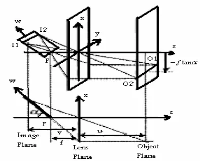
As shown in Fig. 2, the range-finder consists of a single optic lens and a sensor whose plane is tilted by an angle with respect to the optical axis. The sensor plane intersects optical axis at the focal point F. Any object at a distance u from lens projects its focused image on an image plane located at a distance v behind the lens. According to the Gaussian lens law, u is related to v by
v 1 u 1 f
1= +
(1)
where f is the focal length. Therefore, object distance u can be calculated once the image plane distance v has been determined. Since the sensor plane is laid out at an angle, it intersects image plane for a range of u values and the position of the intersection line I1I2 along the w-axis of the sensor plane depends on u.
Note that: 1) line I1I2 is where the best focus is obtained for a given u, 2) this line is a projection of a line O1O2 of the object plane, 3) the focusable object line O1O2 is always on the plane x=-f.tanα, regardless of the value of u. Therefore, the value of v and then u will be determined from the position w of the sensor line of the highest focus.
The lens is made off the shelf and the chip includes photo receptor, focus processor, winner-take-all and distance decoder.
1 - Winner-Take-All
Fig. 2 3D and 2D views of the optic lens and image plane
3 Photo Receptor
A simple non-adaptive source follower logarithmic receptor is shown in Fig. 3(a). The gain is
mV 25.4 q KT
VT= = per e-fold intensity change. The performance of the source follower receptor is deficient in two respects: the high offset and the slow response of the circuit.
On the other hand, one of the biggest problems in photo receptors is small change of output versus big change of input light. Because of requiring high sensitivity for other circuits, it needs to amplify the output. This amplification can be done by an adaptive element in feedback loop. Also, feedback can improve small signal specifications of the system.
The adaptive receptor shown in Fig. 3(b) [12], remedies these problems. It consists of a source follower receptor input stage combined with amplification and low-pass filtered feedback. The output of the source follower receptor is amplified by the inverting amplifier consisting ofQn, andQp. The voltage gain -Aamp is typically several hundred. Qcas is a cascode that nullifies the miller capacitance from the gate to drain ofQn and also doubles the gain of the amplifier.
Fig. 3 Receptor circuits (a) Source follower receptor (b) Adaptive receptor
Photo Receptor Optic
Lens
Winner-Take-All Focus
Processor
Distance Decoder
Detected
Light Display
The input current comes from a photo diode that generates a photo current linearly proportional to intensity [12]. The current consists of a steady-state background component, Ibg , and a varying or transient component, i.
The photo diode is formed as an extension of the source region of the feedback transistorQfb. For typical light intensities, Qfb operates in sub threshold region. The high gain in the feedback loop effectively clampsVP. When the input current changes an e-fold,
f
V must change by VT/k (k is the back-gate
coefficient) to hold VP clamped. So the gain from Vf to VP is k and from i to VP is VT per e-fold intensity change. Also the gain from Vo to Vf is 1 in steady-state and in transient, where the output must feed back to the input through the capacitive divider, isC2/
(
C1+C2)
. The closed-loop gain in steady-state and transient are given by equations (2) & (3).k 1 I i V V A bg T o
cl= = (Steady-state closed-loop gain) (2)
2 2 1 bg T o cl C C C k 1 I i V V
A = = + (Transient closed-loop gain) (3)
Equation (2) is the small signal equivalent of the large signal expression for the steady-state output voltage given by equation (4).
) I i I log( k 1 ) log(I V V 0 bg b T
o = + + (4)
The clamping of the input nodes speeds up the receptor response. The larger the gain Aampof the feedback amplifier, the less the input node needs to move, and the more speed up we obtain. On the other hand, for the given feedback amplifier, the more closed-loop gainAcl, the more the input node must move, and the slower the response. So, we shall take as a base-line, the speed of the source follower receptor. The speed up obtained by using the active feedback to clamp the input node is given by equation (5).
cl amp loop
A A
A = (Speed up) (5)
The speed up is equal to the total loop gain, obtained by multiplying the gain all the way around the loop. The adaptive element is a resistor-like device that has a monotonic I-V relationship. This element acts like a pair of diodes in parallel with opposite polarity. The current increases exponentially with voltage for either sign of voltage, and there is an extremely high resistance region around the origin [12].
The I-V relationship of the expansive element means that the effective resistance of the element too big for small signals and small for large signals. Hence, the adaption is slow for small signals and fast for large
signals. This behavior is useful, because it means that the receptor can adapt quickly to a large change in conditions (moving from shadow to sunlight), while maintaining high sensitivity to small and slowly varying signals.
4 Focus Processor
Each line of the sensor plane is equipped by a focus processor to calculate the degree of focus along that line. The circuit of a 3-pixel focus processor comprising pixels i-1, i and i+1 is shown in Fig. 4. Note that each photo diode drives a pair of NMOS transistors with a common drain. Also note that the diodes shown in Fig. 4 are realized with diode-connected MOSFETs.
Fig. 4A 3-pixel slice of the focus processor
The common-drain currentIiof pixel-i is given by equation (6). )] V (V ) V [(V 2 g I
I i1 i i i1
m B
i = - + - - - - (6)
The difference between IB andIi, approximates the second spatial derivative.
)] V (V ) V [(V 2 g I I
ΔI i1 i i i1
m i B
i@ - = + - - - - (7)
If the second derivative is positive, this current flows out of pixel-i onto bus-1, and if it is negative, this current flows out of bus-2 into pixel-i. These two buses are kept out at virtually constant voltages by two opamps per row and their currents are summed up to generate the sum of absolute value of the second derivatives.
The measurement of focus is representing by SML1:
å
-=
=m1
1 i
i ΔI
SML (8)
The output current of focus processor, that is the sum of bus-1 and bus-2 currents, represents an analog focus measure for each line.
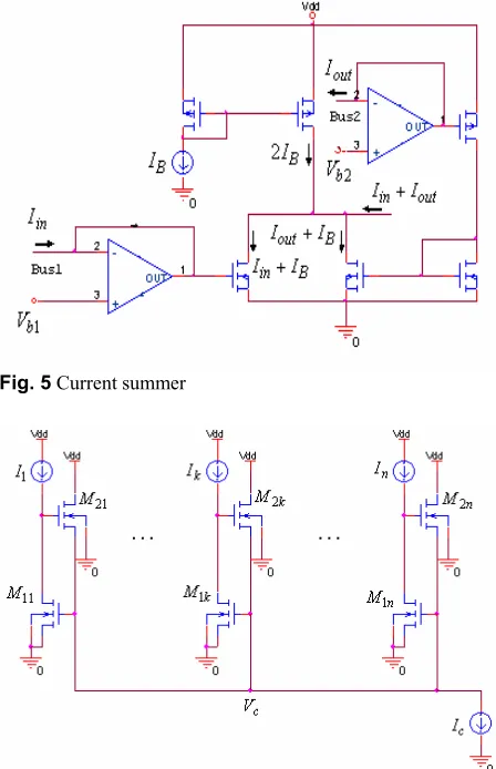
The current summer, which sums the absolute currents of bus-1 and bus-2, is shown in Fig. 5.
1 - Sum of Modified Laplacian
5 Winner-Take-All
Measurements of analog focus for each line, which are output currents of focus processors, are compared in a winner-take-all block. This circuit identifies the line of the highest output current, hence the highest focus. Fig. 6 is a schematic diagram of the winner-take-all circuit [13]. A wire associated with the potentialVC, computes the inhibition for the entire circuit. To compute the global inhibition, each neuron k contributes a current onto this common wire, using transistorM2k. To apply this global inhibition locally, each neuron responds to the common wire voltageVC, using transistorM1k.
Fig. 5Current summer
Fig. 6Schematic diagram of the winner-take-all circuit
For analysis of the circuit, we consider a two-neuron winner-take-all like Fig. 7.
First, we consider the input conditionI1=I2ºIm. Transistors M1 and M2 have identical potentials at gate and source, and are both sinkingIm. Thus, the drain potentials V1and V2must be equal. Transistors M3 and
4
M have identical source, drain and gate potentials, and therefore must sink the identical current
2 I I
I C
C2 C1= = . In the sub threshold region of operation, the
equation ) V V exp( I I 0 C 0
m = describes transistors M1 and 2
M currents. Like wise the
equation ) V V V exp( I 2 I 0 C m 0
C = - , where
2 1
m V V
V º = ,
describes transistors M3 and M4currents. Solving for
m
V versus Imand IC yields the equation (9).
) 2I I ln( V ) I I ln( V V 0 C 0 0 m 0
m= + (9)
Thus, for equal input currents, the circuit produces equal output voltages.
Fig. 7 Schematic diagram of a two-neuron winner-take-all circuit
Now, consider the input condition I1=Im+δi andI2 =Im. Transistor M1 must sink δi more current than in the previous condition. Thus, the gate voltage of
1
M rises. But transistors M1 and M2must have a common gate voltage. So M2must also sinkIm+δi. But only Im is present at the gate ofM2, therefore, the drain voltage ofM2,V2, must decrease. For small value ofδi, the Early effect serves to decrease the current throughM2 and decreasing V2 linearly withδi. For large value ofδi, M2 must leave saturation, driving V2 to approximately 0. So at this condition, IC2 »0
andIC1 »IC. The equation V )
V exp( I δ I 0 C 0 i
m+ = describes
transistor M1 and the equation )
V V V exp( I I 0 C 1 0 C -=
describes transistorM3. Solving for V1 yields the equation (10). ) I I ln( V ) I δ I ln( V V 0 C 0 0 i m 0 1 + + = (10)
The winning output encodes the logarithm of the associated input.
The conductance of transistors M1 and M2determines the losing response of the circuit. The Early voltage,Ve, is related to the conductance of a saturated MOS transistor. L V L V d e ¶ ¶ = (11)
where Vdis the drain potential of a transistor and L is the channel length of a transistor. Thus, the width of the losing response of the circuit depends on the channel length of transistors M1 andM2. Increasing the channel length of transistors M1 andM2, narrows the losing response of the circuit and vise-versa.
6 Digital Distance Decoder
This circuit converts the index of the identified row to distance information. The range-finder must cover the range 1.5m-10m. Since, the photo receptor matrix which is used includes 18 lines and each line has 16 pixels, so the range is estimated in 18 levels and the distance between two successive ranges is 0.5m.
For indicating range information, 8 bits look-up table is designed which the LSB bit is assigned for the decimal digit. Since the decimal digit is 0.5, hence its equal digital value is 1. Also, for a specific u (object distance from lens), one row of photo receptor is selected as a row with highest focus. We consider 8 bits digital code, which equal to distance, for each row.
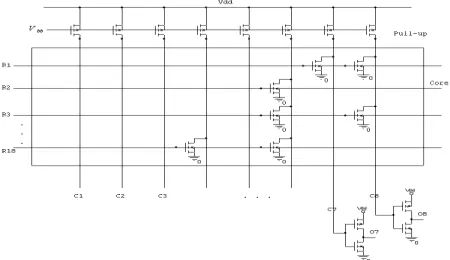
Fig. 8 shows the designed circuit of the look-up table. In this circuit, a bit has been defined by presence or absence of a data from a row to a column. The absence of a path is achieved by no joining element between row and column. MOS switch transistors are used for connecting rows to columns.
Fig. 8Schematic diagram of the look-up table
When a row is selected, (row with highest focus), columns which have NMOS transistors and their gates excite by this row, will be zero. Columns which don't have transistors will be pulled up to
V
dd by pull-uptransistors. Since the 8 bits digital code of each row has been defined, so the position of NMOS transistors in the row will be specified.
For optimizing the number of transistors and improving high and low levels of the outputs for the 8 bits codes, the system has been implemented complement mode; therefore an inverter has been used for each column output or bit.
7 Simulation Results
In this section, the simulated results with HSPICE and 0.35μmCMOS technology parameters for the described units have been presented.
Fig. 9 shows DC sweep simulated result of the photo receptor. Usually the light intensity inside a normal room is below 1 lux, and the level of intensity produces photo current less than 1nA. So, in this simulation, the input photo current has been considered between 0-5nA. According to Fig. 9, for small photo currents which correspond to transient signals, the photo receptor is very sensitive, but for large photo currents which correspond to steady-state signals, the photo receptor is adaptive and has small variations in the output.
Fig. 10 shows the transient signal of the different circuit nodes according to the pulse input with 1nA photo current level.
The transfer function of a slice of the focus processor, as defined by equation (7), is shown in Fig. 11. In this figure, the simulated results of the circuit are interpolated by Matlab.
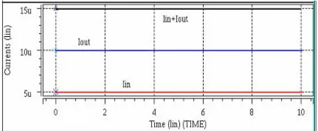
The output current of focus processor, that is the sum of bus-1 and bus-2 currents, is in microamperes range. Fig. 12 shows the simulated results of the current summer according to the inputs Iin=5mA andIout =10mA. Fig. 13
shows the response of this circuit for the pulsing inputs. The simulated results of WTA for two different channel length of transistors M1 and M2 is shown in Fig. 14. Increasing the channel length of transistors M1 andM2, causes a narrow region for the losing response of the circuit.
The simulated results of the distance decoder according to excitation of the first row, which is equal to distance 1.5m and digital code 00000011, is shown in Fig. 15. In this case, two LSB bits O7and O8 are high and another bits are low.
Shown in table-1 and Fig. 16 are the system-level simulation results of the entire system. The output SML of each focus processor and its digital output code of distance for three different object distances are summarized in table-1. The maximum SML belongs to the sensor line that corresponds to the correct distance. Fig. 16 shows the output currents of the 18 focus processors.
Table 2 summarizes the properties of the designed chip.
Fig. 9 The output voltages DC sweep according to input photo current
Fig. 10 Transient variations of different nodes of photo receptor according to 1nA pulse photo current
Fig. 11 DC response of a slice of focus processor
Fig. 12Simulated results of current summer for DC inputs
Fig. 13Simulated results of current summer for pulse inputs
Fig. 14 Simulated results of WTA with two different channel length for transistors M1 and M 2
Fig. 15Simulated results of the distance decoder according to excitation of first row
Fig. 16 Output current of the 18 focus processors for three different object distances
Table 1Output SML of each of the 18 focus processor and their digital output codes Sensor
Line No.
1 2 3 4 5 6 7 8 9 10 11 12 13 14 15 16 17 18 Digital Output code
U=1.5m 38u 26u 19u 3u 0 0 0 0 0 0 0 0 0 0 0 0 0 0 00000011
U=6m 0 0 0 0 12u 15u 17u 22u 24u 43u 30u 25u 11u 3u 0 0 0 0 00001100
U=7.5m 0 0 0 0 0 1.8u 2.1u 2.6u 2.8u 3.5u 13u 17u 38u 33u 20u 7u 3u 0 00001111
Table 2Properties of the chip
1.5-10m (in 18 scales) Range of distance covered
40mW Power consumption
0.35μm-CMOS Technology
5V Power supply
8 Conclusion
The range-finding technique based on the passive imaging is presented that requires seasonable signal processing stages and can be implemented on a single mixed-signal CMOS chip including the photo sensor matrix. The advantages of the proposed method are: a) The processing steps are minimized with comparison of other techniques.
b) The mechanical movement for scanning of the object is not necessary, so the system is optimized for implementing on a single chip.
References
[1] A. Moini, Vision Chips or Seeing Silicon. The University of Adelaide: 1997.
[2] A. Gruss, L. R. Carely and T. Kanade, “Integrated Sensor and Range Finding Analog Signal Processor,” IEEE Journal of Solid-State Circuits, Vol. 26, No. 3, Mar. 1991.
[3] Y. Sato, K. Araki and S. Parthasarathy, “High Speed Range Finder,” Optics, Illumination and Image Sensing for Machine Vision II, SPIE, Vol. 850, pp. 184-188, 1987.
[4] T. Kida, K. Sato and S. Inokuchi, “Real-Time Range Imaging Sensor,” Proc. 5th Sensing Forum, pp. 91-95, Apr. 1988.
[5] G. Surya and M. Subbarao, “Depth from Defocus by Changing Camera Aperture: a Spatial Domain Approach,” Proc. CVPR '93, IEEE Computer Society Conference, pp. 61-67, 1993.
[6] S. K. Nayar, “Shape from Focus System,” Proc. CVPR '92, IEEE Computer Society Conference, pp. 302-308, 1992.
[7] A. Castano and N. Ahuja, “Omni Focused 3D Display Using the Non-Frontal Imaging Camera,” Proc. IEEE and ATR Workshop, pp. 28-34, 1998. [8] M. Subbarao and J. K. Tyan, “Selecting the
Optimal Focus Measure for Auto-Focusing and Depth-From-Focus,” IEEE Trans. on PAMI., Vol. 20, No. 8, pp. 870–884, 1998.
[9] M. Subbarao and T. Choi, “Accurate Recovery of 3D Shape from Image Focus,” IEEE Trans. on PAMI, Vol. 173, pp. 266-274, 1995.
[10] S. K. Nayar and Y. Nakagawa, “Shape from Focus,” IEEE Trans. on PAMI, Vol. 168, pp. 824-831, 1994.
[11] S. K. Nayar and M. Watanabe, “Real-Time Focus Range Sensor,” IEEE Trans on PAMI, Vol. 1812, pp. 1186-1198, 1996.
[12] T. Delbruck and C. A. Mead, Adaptive Photo Receptor with Dynamic Range. Dept. of Computation and Neural Systems, CIT.
[13] J. Lazzaro and S. Reychebusch, Advances in Neural Information Processing Systems. San Mateo, CA: Morgan Kaufmann, 1989, pp. 703-711.