Abstract- Introduction of reference frames in the analysis of electrical machines has turned out not only to be useful in their analysis but also has provided a powerful tool for the implementation of sophisticated control techniques. This application note gives an introduction to the theory of the most commonly used reference frames and provides routines that allow for easy conversion amongst them. Control of three-phase power converters in the synchronous reference frame is now a mature and well developed research topic. However, for single-phase converters, it is not as wellestablished as three-phase applications. The SBI can produce an ac output voltage that is either greater or less than the available dc input voltage. Also, the SBI exhibits better electromagnetic interference noise immunity when compared to the VSI, which enables compact design of the power converter. These features make the SBI suitable for dc nanogrid applications. The developed theory of reference frames is equally applicable to the synchronous machines. This machine is sometimes known as the sinusoidal brushless machines or the brushless ac machine and is very popular as a high-performance. This paper also presents a dq synchronous reference- frame-based controller for SBI, which regulates both dc and ac bus voltages of the nanogrid to their respective reference values under steady state as well as under dynamic load variation in the nanogrid.
Index Terms—photovoltaic system, DC nanogrid, switched boost inverter (SBI), synchronous reference frame (SRF).
I. INTRODUCTION
Distributed generation using renewable energy sources is gaining popularity due to environmental concerns over burning fossil fuels, deregulation of the electricity industry, and technological advances in power electronics and renewable energy sources. Natural resources can be connected directly to the grid by means of a grid-tied inverter. Another option is to combine renewable generation with local loads to form an independent power system [1]. A nano-grid is defined an aggregation of local small scale
Manuscript received Feb, 2016.
S.Manikandan, UG Student, Department of EEE, PSN College of Engg. and Tech., Tirunelveli, Tamilnadu.
S.Rajagopalan
,
UG Student, Department of EEE, PSN College of Engg. and Tech., Tirunelveli, Tamilnadu.D.Vinothkumar
,
UG Student, Department of EEE, PSN College of Engg. and Tech., Tirunelveli, Tamilnadu.Ms.X.MonicaRoselin, Assistant Professor, Department of EEE, PSN College of Engg. and Tech., Tirunelveli, Tamilnadu.
M.Muneeswaran, Assistant Professor, Department of EEE, PSN College of Engg. and Tech., Tirunelveli, Tamilnadu.
generators and loads. The load on a nanogrid is typically less than 20 kW, as in the case of a small rural community or industrial site, and the loads are located within 5 km of the picosources. The generators are primarily based on clean forms of energy such as fuel cells, solar arrays, and wind turbines. If a nanogrid has sufficient generation and storage, it can operate as an independent power island. However, a nanogrid can be connected to the grid to export excess power and to eliminate the need for energy storage.
Renewable generation, excluding wind power, is currently more expensive than central generation. In the future, however, nanogrids may find a niche in New Zealand's rural power system, where the cost of power is expected to increase due to a deregulated electricity market. Nanogrids may become a viable method of deferring upgrades and providing voltage support to the weak network.
A nanogrid can be controlled in a decentralised fashion, with each picosource controlling its power output based on local information available at the terminals. Decentralised control is fast and reliable, as it does not require control interconnections, but optimising the efficiency and overall operation of the nanogrid can be difficult. Another option is central control, which requires a powerful controller and fast communications link to simultaneously control the output of each generator. This strategy allows optimisation of the system, but compromises the system’s reliability since the system is dependent on a single controller and communication system.
Fig.1. Structure of an interconnected nanogrid
In the nanogrid structure of Fig. 1, three different power converter stages are used to interface the renewable energy source, energy storage unit, and the local ac loads in the system to the dc bus. This paper proposes a structure of the dc nanogrid using switched boost inverter (SBI) [4]–[6] as a power electronic interface. Fig. 2 shows the structure of the
Switched Boost Inverter for Grid Connected and
Nanogrid Applications in Standalone DC
proposed SBIbased dc nanogrid, and Fig. 3 shows the circuit diagram of the SBI supplying both dc and ac loads.
Fig.2. Structure of the proposed SBI-based dc nanogrid.
Fig. 2 shows structure of the proposed SBIbased dc nanogrid which has the following advantages when compared to the conventional structure.SBI is a single-stage power converter that can supply both dc (between node VDC and ground) and ac loads (between nodes AO and BO) simultaneously from a single dc input. So, it can realize both the dc-to-dc converter for solar panel and the dc-to-ac converter in a single stage. This decreases size and cost of overall system. The output ac voltage of SBI can be either higher or lower than the available source voltage. So, it has wide range of obtainable output voltage for a given source voltage.SBI exhibits better electromagnetic interference (EMI) noise immunity when compared to a traditional voltage source inverter (VSI), as the shoot-through (both switches in one leg of the inverter bridge are turned ON simultaneously) due to EMI noise will not damage the inverter switches [4]. This reduces extra burden on the power converter protection circuit and helps in realization of compact design of the power converter. As the SBI allows shoot-through in the inverter legs, it does not require a dead-time circuit and hence eliminates the need for complex dead-time compensation technologies.
Fig.3. Circuit diagram of SBI supplying both dc and ac loads.
As shown in Fig. 3, the SBI has one active switch (S), two diodes (Da ,Db ), one inductor (L), and one capacitor (C) connected between voltage source Vg and the inverter bridge. A low-pass LC filter is used at the output of the inverter bridge to filter the switching frequency components in the inverter output voltage vAB. As shown in Fig. 3, the capacitor C (connected between node VDC and ground) of SBI acts as a dc bus for dc loads while the capacitor
Cf(connected between nodes AO and BO) of SBI acts as an ac bus for ac loads. The operating principle and pulsewidth modulation (PWM) control of the SBI.
II. SWITCHEDBOOSTINVERTERTOPOLOGY
SBI is a single-stage power converter derived from Inverse Watkins Johnson (IWJ) Topology. This topology exhibits properties similar to that of a Z-source inverter (ZSI) with lower number of passive components and more active
components. This section presents a review of the approach used to derive the SBI from IWJ topology. A detailed comparison of SBI with a traditional two-stage dc-to-ac conversion system is also given in this section.
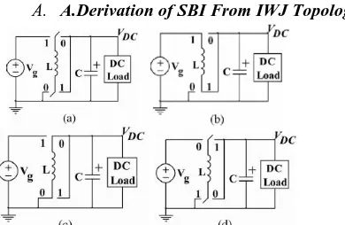
A. A.Derivation of SBI From IWJ Topology
Fig.4. (a) Schematic of IWJ topology. (b) Equivalent circuit of IWJ topology in D·TS interval. (c) Equivalent circuit of IWJ topology in (1 – D)·TS interval.
(d) CIWJ topology.
The schematic of IWJ converter is shown in Fig. 4(a) and its equivalent circuits in D·TS and (1 – D)·TS intervals of a switching cycle TS are shown in Fig. 4(b) and (c), respectively. As shown in Fig. 4(b), during D·TS interval, the two switches of the converter are in position 1, and inductor L
is connected between the input and the output. Similarly, during (1 – D)·TS interval, the switches are in position 0 and the inductor is connected between the output and the ground, as shown in Fig. 4(c). Interchanging the D·TS (position 1), and (1 – D)·TS (position 0) intervals of IWJ converter leads to Fig. 4(d).
This configuration is named as the complementary IWJ (CIWJ) topology. Note that this interchange has no impact on the states of the converter. However, as far as implementation is concerned, this will imply that the controlled switch and diode of CIWJ and IWJ are interchanged.
Fig.5. (a) Realization of CIWJ topology using power semiconductor devices.(b) Connection of a VSI across the dc output node VDC of CIWJ topology.(c) Connection of a VSI across the switching terminal Vi of the CIWJ topology
combination requires only controlled switch S apart from the inverter bridge. The switch Si of CIWJ topology can be realized by utilizing the shoot-through state of the inverter bridge. Also, similar to the cascaded connection shown in Fig. 5(b), this circuit can also supply a dc load (at the output of CIWJ) and an ac load (at the output of the inverter bridge) simultaneously from a single dc voltage source Vg . The circuit of Fig. 5(c) is named as SBI topology in [4]. Note that it is not a direct cascade connection of CIWJ topology and VSI, as the inverter bridge is connected at a switch node of CIWJ converter but not at its output terminal. When compared to the cascaded connection shown in Fig. 5(b), the SBI has following advantages:
1)
In the event of shoot-through in any phase leg of the inverter bridge, the diode Db is reversebiased and capacitorC is disconnected from the inverter bridge. Now, the current through the circuit is limited by the inductor L. So, similar to ZSI, shoot-through does not damage the switches of the SBI also.
2)
As the SBI allows shoot-through, no deadtime is needed to protect the converter. Also this circuit exhibits better EMI noise immunity compared to a traditional VSI.3)
Since dead-time is not required, there is no need of extra dead-time compensation technologies to compensate the waveform distortion caused by dead-time.III.STEADY-STATEANALYSISANDPWMCONTROL
OFSBISUPPLYINGBOTHDCANDACLOADS
B. A. Steady-State Analysis of SBI
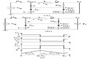
The circuit diagram of SBI supplying both dc and ac loads is shown in Fig. 3. Fig. 6(a) and (b) shows the equivalent circuits of SBI during the shoot-through interval D·TS and non-shoot through interval (1 – D)·TS of the inverter bridge, respectively. As shown in Fig. 6(a), during D·TS interval, the inverter is in shootthrough zero state and switch S is turned ON.
The diodes Da and Db are reverse biased as VDC
> Vg. In this interval, capacitor C charges the inductor L
through switch S and the inverter bridge. So, the inductor current equals the capacitor discharging current minus the dc load current.
Fig.6. (a) Equivalent circuit of SBI in D·TS interval. (b) Equivalent circuit of SBI in (1 – D)·TS interval. (c) Steady-state waveforms.
During (1 – D) ·TS interval, the inverter is in non-shoot through state and the switch S is turned OFF. The inverter bridge is represented by a current source in this interval as shown in the equivalent circuit of Fig. 6(b). Now, the voltage source Vg and inductor L together supply power to the dc load, inverter, and the capacitor through diodes Daand Db.
The inductor current in this interval equals the capacitor charging current added to the inverter input current and the dc load current. Note that the inductor current is assumed to be sufficient enough for the continuous conduction of the diodes Da, Db for the entire interval (1 – D)·TS . Fig. 6(c) shows the steady-state waveforms of the converter operation for one switching cycle TS with respect to the gate control signal GS of switch S.
(1)
(2)
(3) The average dc link voltage Vi can be calculated as
(4)
IV. CLOSED-LOOP CONTROL OF SBI
Fig.7 shows the closed-loop control architecture of the SBI supplying both dc and ac loads. In this scheme, the task of the controller is to generate gate control signals (GS ,GS 1 , GS 2 ,GS 3 , and GS 4 ) for SBI shown in Fig. 3 such that the voltages at the dc bus (VDC) and the ac bus (VAC) are
regulated to their respective reference values and .. As shown in
Fig.7, the controller for the dc nanogrid has been implemented in digital domain using Texas Instruments TMS320F28335 DSP.
Fig.7. Closed-loop control architecture of the dc nanogrid.
This DSP has a built-in 12-bit analog-to-digital converter that accepts analog feedback signals from SBI and converts them into digital domain. These feedback signals along with the reference signals for the ac and dc bus voltages are given as inputs to the controller block. The controller block has two separate control loops for controlling the dc bus voltage VDC
and ac bus voltage The controller block has two separate control loops for controlling the dc bus voltage VDC and ac
bus voltage VAC. The ac bus voltage controller has a cascaded
control structure with an inner current control loop and an outer voltage control loop. Note that, as the ac bus voltage controller is designed using SRF approach the reference for ac bus voltage 𝑉∗
AC is directly given in dqdomain in Fig.8, in
order to reduce the extra computational burden on the DSP.
V.PHOTOVOLTAIC(PV)SYSTEM
PV cell. Cells may be grouped to form arrays. The voltage and current available at the terminals of a PV device may directly feed small loads such as lighting systems and DC motors or connect to a grid by using proper energy conversion devices.
C. Fig.8. Block diagram representation of Photovoltaic system
This photovoltaic system consists of three main parts which are PV module, balance of system and load. The major balance of system components in this systems are charger, battery and inverter. The Block diagram of the PV system is shown in Fig.8.
A. Photovoltaic cell A photovoltaic cell is basically a semiconductor diode whose p–n junction is exposed to light. Photovoltaic cells are made of several types of semiconductors using different manufacturing processes. The incidence of light on the cell generates charge carriers that originate an electric current if the cell is short circuited1
D. Fig.9. Practical PV device
The equivalent circuit of PV cell is shown in the fig.9. In the above figure the PV cell is represented by a current source in parallel with diode. Rs and Rp represent series and parallel resistance respectively. The output current and voltage form PV cell are represented by I and V. The I-V characteristics of PV cell are shown in fig.11. The net cell current I is composed of the light generated current IPV and the diode current ID.
E. Fig.10. Characteristics I-V curve of the PV cell VI. Fuel Cell Operation
Pressurized hydrogen gas (H2) enters cell on anode side. Gas
is forced through catalyst by pressure. When H2 molecule
comes contacts platinum catalyst, it splits into two H+ ions and two electrons (e-). Electrons are conducted through the anode. Make their way through the external circuit (doing useful work such as turning a motor) and return to the cathode side of the fuel cell. On the cathode side, oxygen gas (O2) is
forced through the catalyst Forms two oxygen atoms, each with a strong negative charge. Negative charge attracts the two H+ ions through the membrane, Combine with an oxygen atom and two electrons from the external circuit to form a water molecule (H2O).
How a fuel cell works: In the polymer electrolyte membrane (PEM) fuel cell, also known as a proton-exchange membrane cell, a catalyst in the anode separates hydrogen atoms into protons and electrons. The membrane in the center transports the protons to the cathode, leaving the electrons behind. The electrons flow through a circuit to the cathode, forming an electric current to do useful work. In the cathode, another catalyst helps the electrons, hydrogen nuclei and oxygen from the air recombine. When the input is pure hydrogen, the exhaust consists of water vapor. In fuel cells using hydrocarbon fuels the exhaust is water and carbon dioxide. Cornell's new research is aimed at finding lighter, cheaper and more efficient materials for the catalysts and membranes. A.Parts of a Fuel Cell
1)
Anode
•
Negative post of the fuel cell.•
Conducts the electrons that are freed from the hydrogen molecules so that they can be used in an external circuit.•
Etched channels disperse hydrogen gas over the surface of catalyst.2)
Cathode
•
Positive post of the fuel cell•
Etched channels distribute oxygen to the surface of the catalyst.•
Conducts electrons back from the external circuit to the catalyst•
Recombine with the hydrogen ions and oxygen to form water.3)
Electrolyte•
Proton exchange membrane.•
Specially treated material, only conducts positively charged ions.•
Membrane blocks electrons.4)
Catalyst
•
Special material that facilitates reaction of oxygen and hydrogen•
Usually platinum powder very thinly coated onto carbon paper or cloth.•
Rough & porous maximizes surface area exposed to hydrogen or oxygen•
The platinum-coated side of the catalyst faces the PEM.VII.MATLABMODELINGANDSIMULATION
RESULTS
Performance of the ClosedLoop Control System with a Step Change in the Load. 3) Performance of SBI with an RL and Rectifier Loads. 4) Operation of SBI with an Isolation Transformer using PV Cell.
F. Case 1: Operation of SBI with an Isolation Transformer
Fig.11 Matlab/Simulink Model of Proposed Switched Boost Inverter with an Isolation Transformer
Fig.11 shows the Matlab/Simulink Model of Proposed Switched Boost Inverter with an Isolation Transformer using Matlab/Simulink Platform.
Fig.12 Steady-state operation of SBI with an isolation transformer, input voltage Vg , dc load voltage VDC , ac output voltage of SBI VAC and ac load
voltage
Fig.12 shows the Steady-state operation of SBI with an isolation transformer, input voltage Vg , dc load voltage VDC ,
ac output voltage of SBI VAC , and ac load voltage.
Fig.13 Steady-state operation of SBI with an isolation transformer, switch node 1 voltage Vsn1 , input voltage of the inverter bridge Vi, and Output voltage of H-Bridge VAB.
Fig.13 shows the Steady-state operation of SBI with an isolation transformer, switch node 1 voltage Vsn1, input
voltage of the inverter bridge Vi, and Output voltage of H-Bridge VAB. Case 2: (a) Performance of the Closed-Loop Control System with a Step Change in the AC
G. Load
Fig.14 Matlab/Simulink Model of Proposed Switched Boost Inverter with a Closed Loop Control System with a Step Change in AC Load.
Fig.14 shows the Matlab/Simulink Model of Proposed Switched Boost Inverter with a Closed Loop Control System with a Step Change in AC Load.
1) Fig.15 Steady-state operation of SBI with Closed Loop Control
System with a Step Change in AC Load, input voltage Vg , dc load voltage VDC , ac output voltage of SBI VAC
Fig.15 shows the Steady-state operation of SBI with Closed Loop Control System with a Step Change in AC Load, input voltage Vg , dc load voltage VDC , ac output voltage of SBI
VAC(b) Performance of the Closed-Loop Control
H. System with a Step Change in the DC Load
Fig.16 Matlab/Simulink Model of Proposed Switched Boost Inverter with a Closed Loop Control System with a Step Change in DC Load.
1) Fig.17 Steady-state operation of SBI with Closed Loop Control
System with a Step Change in DC Load, input voltage Vg , dc load voltage VDC , ac output voltage of SBI VAC
Fig.17 shows the Steady-state operation of SBI with Closed Loop Control System with a Step Change in DC Load, input voltage Vg , dc load voltage VDC , ac output voltage of SBI
VAC, and Vpri switch node voltage.
Case 3: Performance of SBI with an RL and Rectifier Loads (a). RL Load:
Fig.18 Matlab/Simulink Model of Proposed Switched Boost Inverter with a RL Load
Fig.18 shows the Matlab/Simulink Model of Proposed Switched Boost Inverter with a RL Load.
(b)
Fig.19 Steady-state operation of SBI with a RL Load, (a) Input Voltage (Vg), Output Voltage Vdc), Ac Voltage (Vac) (b) Vac&Iac
Fig.19 shows the Steady-state operation of SBI with a RL Load, (a) Input Voltage (Vg), Output Voltage Vdc), Ac Voltage (Vac) (b) Vac&Iac. (b). Rectifier Load:
Fig.20 Matlab/Simulink Model of Proposed Switched Boost Inverter with a Rectifier Load
Fig.20 shows the Matlab/Simulink Model of Proposed Switched Boost Inverter with a
Rectifier Load.
(b)
Fig.21 Steady-state operation of SBI with a Rectifier Load, (a) Input Voltage (Vg), Output Voltage Vdc), Ac Voltage (Vac) (b) Vac&Iac
Fig.21 shows the Steady-state operation of SBI with a Rectifier Load, (a) Input Voltage (Vg), Output Voltage Vdc), Ac Voltage (Vac) (b) Vac&Iac.
I. Case 4: Operation of SBI with an Isolation Transformer using PV Cell
Fig.22 Matlab/Simulink Model of Proposed Switched Boost Inverter with an Isolation Transformer with PV Model
Fig.22 shows the Matlab/Simulink Model of Proposed Switched Boost Inverter with an Isolation Transformer with PV Model using Matlab/Simulink Platform.
(a)
Fig.23 Steady-state operation of SBI with an isolation transformer with PV Model, input voltage Vg , dc load voltage VDC , ac output voltage of SBI
VAC , and ac load voltage
Fig.23 shows the Steady-state operation of SBI with an isolation transformer with PV Model, input voltage Vg , dc load voltage VDC , ac output voltage of SBI VAC , and ac load
voltage.
Fig.24 Steady-state operation of SBI with an isolation transformer, switch node 1 voltage Vsn1 , input voltage of the inverter bridge Vi, and Output voltage of H-Bridge VAB.
Fig.24 shows the Steady-state operation of SBI with an isolation transformer, switch node 1 voltage Vsn1, input voltage of the inverter bridge Vi, and Output voltage of H-Bridge VAB.
VIII.CONCLUSION
This paper presents a novel power electronic interface called switched boost inverter (SBI) for dc nanogrid applications with the combination of Photovoltaic Cell. It is supply both dc and ac loads simultaneously from a single dc input. It is also proven that the SBI can generate an acoutput voltage that is either higher or lower than the available source voltage. This paper also describes the advantages and limitations of SBI when compared to the ZSI and the traditional two stage dc-to-ac conversion system. The steadystate and small-signal analysis of the SBI supplying both dc and ac loads, and a PWM control technique suitable for SBI are also described in this paper. Also, the analysis and design of a SRF-based controller that regulates both the dc and ac bus voltages of SBI to their respective reference values has been discussed in this paper. The performance of SBI has been tested using simulation with an isolation transformer and also with three different types of ac loads: R, RL, and nonlinear loads. It can be concluded from the simulation results that the control strategy of SBI shows excellent performance during steady state as well as during a step change in either dc or ac load in the system. These results confirm the suitability of SBI and its closed-loop control strategy for dc nanogrid applications with PV Source.
REFERENCES
[1] S. H. Hwang and J. M. Kim, “Dead-time compensation method voltage fed PWM inverter,” IEEE Trans. Energy Convers., vol. 25, no. 1, pp. 1–10, Mar. 2010.
[2] F. Gao, P. C. Loh, R. Teodorescu, and F. Blaabjerg, “Diode-assisted buck– boost voltage-source inverters,” IEEE Trans. Power Electron., vol. 24, no. 9, pp. 2057–2064, Sep. 2009.
[3] A. A. Fardoun and E. H. Ismail, “Ultra step-up DC–DC converter with reduced switch stress,” IEEE Trans. Ind. Appl., vol. 46, no. 5, pp. 2025– 2034, Sep./Oct. 2010.
[4] J. Liu, J. Hu, and L. Xu, “Dynamic modeling and analysis of Z sourceconverter-derivation of AC small signal model and designorientedanalysis,”IEEE Trans. Power Electron., vol. 22, no. 5, pp. 1786–1796, Sep.2007.
[5] D. G. Holmes and T. A. Lipo, Pulse Width Modulation for Power Converters:Principles and Practice. Piscataway, NJ: IEEE Press, 2003.[6] R. W. Erickson and D. Maksimovic, Fundamentals of Power Electronics,2nd ed. Norwell, MA: Kluwer, Jan. 2001.
[7] N. Mohan, T. Undeland, and W. Robbins, Power Electronics: Converters, Applications and Design, 2nd ed. New York: Wiley, 1995. [8] Y. Huang, M. Shen, F. Z. Peng, and J. Wang, “Z-source inverter forresidential photovoltaic systems,” IEEE Trans. Power Electron., vol. 21, no. 6, pp. 1776–1782, Nov. 2006.
[9] R. J. Wai, C. Y. Lin, R. Y. Duan, and Y. R. Chang, “High-efficiency DCDC converter with high voltage gain and reduced switch stress,” IEEE Trans. Ind. Electron., vol. 54, no. 1, pp. 354–364, Feb. 2007. [10] U. A. Miranda, M. Aredes, and L. G. B. Rolim, “A DQ synchronous reference frame current control for single-phase converters,” in Proc. 36th IEEE Power Electron. Specialists Conf. (PESC), Recife, Brazil, Jun. 2005, pp. 1377–1381.