REVIEW ARTICLE
DESIGN OF LOW POWER NETWORK ON CHIP USING DATA ENCODING TECHNIQUES
*Arivoli, S.
Department of Electrical and Electronics Engineering, V.S.B College of Engineering Technical Campus,
Coimbatore, TamilNadu, India
ARTICLE INFO ABSTRACT
An electronic circuit might consist of a CPU, ROM, RAM and other glue logic. VLSI lets IC makers at all of this into one chip. A contrast of Network On Chip’s (NoC’s) structure makes a fitting replacement for System On Chip (SoC) design in designs incorporating large number of processing cores. In NoC the overall power dissipation is due to the interconnection system. The interconnects have become main element in dynamic power dissipation in a NoC design. NoC improves the scalability of SoC and the power efficient of complex SoC compared to other designs. The wires in the links of the NoC are shared by many signals. The project concept depends on the traffic flow in the chip. The idea presented in this project exploits the wormhole switching techniques and works on an end to end basis. That is flits are encoded by the Network Interface (NI) before they are injected in the network and are decoded by the destination NI. In such a way as to minimize both switching activity and the coupling switching activity which represent the main factors of power dissipation. The proposed schemes are general and transparent with respect to the underlying NoC fabrication. The data encoding technique in which number of switching transitions in data word is brought down to reduce the power dissipation. To verify the efficiency of the proposed technique, encoder structure was designed by using VerilogHDL. As result, we save the power on NoC links more than 50%.
INTRODUCTION
Very-large-scale integration (VLSI) is the process of creating an integrated circuit(IC) by combining thousands of transistors into a single chip. Before the introduction of VLSI technology, most ICs had a limited set of functions they could perform. An electronic circuit might consist of a CPU, ROM, RAM and other glue logic. As the complexity of circuit was dependent on speed. If the component of the circuit were too large or the wires interconnecting them too long. The electric signal could not travel fast enough through the circuit. Jack Kilby at Texas Instruments found a solution to this problem in 1958. In September 1958, he had his first integrated circuit ready. Although the first integrated circuit was crude and had some problems, the idea was ground breaking. By making all the parts out of the same block of material and adding the metal needed to connect them as a layer on top of it, there was no need for discrete components. No more wires and components had to be assembled manually. The circuits could be made smaller, and the manufacturing process could be automated. From here, the idea of integrating all components on a single silicon wafer came into existence, which led to development in small-scale integration (SSI) in the early 1960s, Medium Scale Integration (MSI) in the late 1960s, further improvement leads to Large Scale Integration (LSI) as well as Very Large Scale Integration (VLSI).
*Corresponding author: Arivoli, S.
Department of Electrical and Electronics Engineering, V.S.B College of Engineering Technical Campus, Coimbatore, TamilNadu, India.
In the 1970’s and 1980’s with ten of thousands of transistors on a single chip [Later hundreds of thousands then million and now billion (10^9)]. The most frequently cited trend is in integration level, which is usually expressed as Moore’s law (the number of components per chip doubles every eighteen months). The most significant for society is the decreasing cost, pre function which has lead to significant improvements of productive and quality of life through proliferation of computers, electronics communication and consumer electronics.VLSI circuit design inherently consists of power, speed, and area constraints. With changing market needs, emphasis is shifting towards power aware and high performance circuit designs.
SYSTEM DESCRIPTION
NoC technology is often called “a front-end solution to a back-end problem.”As semiconductor transistor dimensions shrink and increasing amounts of IP block functions are added to a chip, the physical infrastructure that carries data on the chip and guarantees quality of service begins to crumble. To meet the growing computation-intensive applications and the needs of low-power, high-performance systems, the number of computing resources in single-chip has enormously increased, because current VLSI technology can support such an extensive integration of transistors. In most System-on-Chip applications, a shared bus interconnection which needs arbitration logic to serialize several bus access requests, is adopted to communicate with each integrated processing unit
Article History:
Received 24th January, 2017
Received in revised form
15th February, 2017
Accepted 14th March, 2017
Published online 30th April, 2017
www.ijramr.com
International Journal of Recent Advances in Multidisciplinary Research
Vol. 04, Issue 04, pp.2468-2475, April, 2017
Keywords:
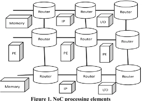
because of its low-cost and simple control characteristics. Such scalable bandwidth requirement can be satisfied by using on-chip packet-switched micro-network of interconnects, generally known as Network-on-Chip (NoC) architecture. The scalable and modular nature of NoC and their support for efficient on-chip communication lead to NoC-based system implementations. In order to meet typical SoC or multi-core processing environment, basic module of network interconnection like switching logic, routing algorithm and its packet definition should be light-weighted to result in easily implemental solutions. NoC processing elements are shown in Figure 1.
Figure 1. NoC processing elements
In communication between several cores in System-on-Chip (SoC) environment, some prevailing mechanisms for this purpose are several bus-based architectures and point-to-point communication methodologies. For simplicity and ease of use, the bus-based architectures are the most common. However, in bus-based architecture, it has fundamentally some limitation in bandwidth, i.e. while the number of components attached to the bus is increased, a physical capacitance on the bus wires grows and as a result its wiring delay grows even further. Another approach to exceed such a limitation of communication and overcome such an enormous wiring delay in future technology is to adopt network-like interconnections which is called Network-on-Chip (NoC) architecture. By applying network on chip communication which inserts some routers in-between each communication object, the required wiring can be shortened. Therefore, the switch-based interconnection mechanism provides a lot of scalability and freedom from the limitation of complex wiring.
Figure 2. End-to-End Process
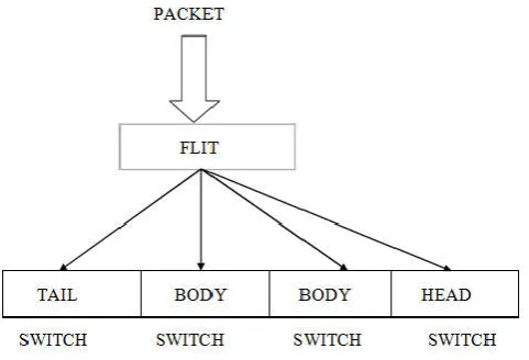
The general scheme of proposed work is given in Figure 2. The basic concept apply the encoding technique is end to end process. In end to end process the NI augmented with an encoder [E] and decoder [D] block. The most suitable switching techniques for on chip communication is wormhole switching. The pipeline nature is the basic concept for the wormhole switching. In wormhole switching the packet is converted into number of flits. The flits delivered in a pipeline. The flit has head, body and tail. The header flit contains control information (destination address, packet size). With the exception of the header flits, the encoder encodes the outgoing flits in such a way as to minimize the power dissipation. Since the routers are not equipped with any encoding logic. The links of the routing paths are cross by the same sequences of flit, the encoding scheme ensure the same switching behavior in each routing path.
of data arrivals (ii) E (SW) which determines how many transitions each arrival will generate. Switching activity is reduced by selecting proper algorithms architecture optimization, proper choice of logic topology, logic level optimization which results in less power.
Software requirements
The software requirements are Modelsim-Altera and Xilinx ISE Design suite. For a long time, programming languages such as FORTRAN, Pascal, and C were being used to describe computer programs that were sequential in nature. Similarly, in the digital design field, designers felt the need for a standard language to describe digital circuits. Thus Hardware Description Languages (HDLs) come into existence. HDLs allowed the designers to model the concurrency of process found in hardware elements. Designers can be described at a very abstract level by use of HDLs. Designers can write their RTL description without choosing a specific topology. Logic synthesis tools can automatically convert the design to any fabrication technology. By describing in HDLs, functional verification of the design can be done early in the design cycle. Since designers work at the RTL level, they can optimize and modify the RTL description until it meets the desired functionality. Designing the HDLs analogous to computer programming. A textual description with comments is an easier way to develop and debug circuits. A Verilog hardware descriptive language is in use in the industry today for Very Large Scale Integration (VLSI) of chips. Verilog HDL is a general purpose HDL that is easy to use and learn. It is similar in syntax to the C programming language. Verilog HDL allows different levels of abstraction to be mixed in the same model. Most popular logic synthesis tool support Verilog HDL. This makes it language of choice for designers. All fabrication venders provide Verilog HDL libraries for post logic synthesis simulation. Thus, designing a chip in Verilog HDL allows the widest choice of venders. Verilog HDL allows a hardware designers to describe designs at a high level of abstraction such as at the architectural or behavioral level as well as the lower implementation levels(i.e.,gate and switch levels) leading to Very Large Scale Integration(VLSI) Integrated Circuits(IC) layouts and chip fabrication. A primary use of HDLs is the simulation of designs before the designer must commit to fabrication.
System design
The functionality of a NoC is defined by how the networks are arranged and how the data is transported from an origin to a target through the network. These concepts are required to be considered when designing a NoC. These NoC design concepts can be categorized as routing strategies, flow control, topology and switching techniques.
(a) Routing Strategies: The path that is to be traversed by a
data packet when transmitted from a source to a destination terminal is defined by a routing strategy. Depending on the topology of the network, there could either only a single path or multiple paths from each source to target terminal .The purpose of a good routing strategy is to provide such a path for data so as to balance the load uniformly across channels irrespective of how the traffic pattern is going to be. The Routing Strategies have to be such that there must be no
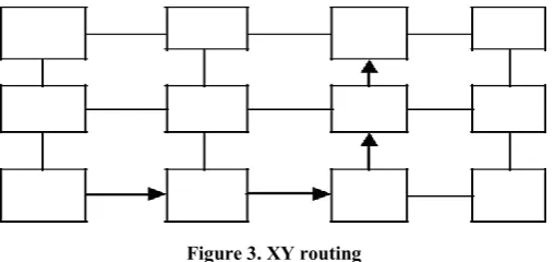
occurrence of livelock, deadlock and starvation situations. Livelock occurs when the packets are continuously moving around in the network without any headway towards the target. When a condition is reached where different routers are waiting for access to resources which have not yet been released by the other router, no forward occurs and this condition is defined as deadlock. Suppose an out channel is constantly allocated to a packet, and some other packet in the buffer needs this channel, this packet gets blocked and a condition called starvation occurs. Routing can be more clearly elucidated with the help of an example of XY-routing. In this, the packets are first directed along X line till they reach the y-coordinate of the target, and afterwards along Y line, as shown in Figure 3. If in between, some channel between two routers is in use by some other packet, the former packet has to wait in the buffer of the router until the channel is free.
Figure 3. XY routing
(b) Flow Control: When packets are traversing on a path, the granting of resources to them is managed by the concept known as Flow Control. With reference to NoC, the most essential resources are channels and buffers in routers. Buffers are responsible for providing temporary storage to packets when they are waiting in a router for a channel to traverse to the next router. To perfectly utilize a NoC, this concept must avoid conflicts with respect to resources that can hold a channel free. In other words, if a packet is waiting on a buffer behind a packet waiting for a busy channel, it should not be blocked if it needs to go onto an idle channel. A good flow control strategy is fair and avoids deadlock. An unfair flow control strategy can cause a packet to wait indefinitely.
Bus, and Star. Mesh Topology is one of the most regular topologies architecture in which each router, apart from that at ends and corners, is linked to four adjoining routers and one processing element, by the way of communication channels. This topology shown in figure 4 allows incorporation of many IP cores in a regular-shape structure. But it has a limitation is in the sense that it has a greater diameter.
Figure 4. Mesh topology
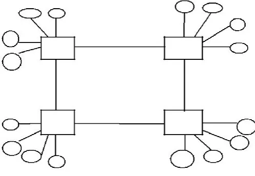
Concentrated Mesh (CMesh) Topology was proposed to reduce diameter of mesh by connecting four cores to a single router as shown in figure 5. The limitation with this topology is that it required long links and connectivity of each router.
Figure 5. CMesh topology
Bus topology is used in local area networks where, each node is connected to a single cable. Each computer or server is connected to the single bus cable shown in figure 6. A signal from the source travels in both directions to all machines connected on the bus cable until it finds the intended recipient. If the machine address does not match the intended address for the data, the machine ignores the data. Alternatively, if the data matches the machine address, the data is accepted. Since the bus topology consists of only one wire, it is rather inexpensive to implement when compared to other topologies. However, the low cost of implementing the technology is offset by the high cost of managing the network. Additionally, since only one cable is utilized, it can be the single point of failure. If the network cable is terminated on both ends and when without termination data transfer stop and when cable breaks, the entire network will be down.
Figure 6. Bus Topology
Linear bus topology: The type of network topology in which all of the nodes of the network are connected to a common transmission medium which has exactly two end points (this is the 'bus', which is also commonly referred to as the backbone, or trunk) – all data that is transmitted between nodes in the network is transmitted over this common transmission medium and is able to be received by all nodes in the network simultaneously. When the electrical signal reaches the end of the bus, the signal "echoes" back down the line, causing unwanted interference. As a solution, the two endpoints of the bus are normally terminated with a device called a terminator that prevents this echo. Distributed bus topology: The type of network topology in which all of the nodes of the network are connected to a common transmission medium which has more than two endpoints that are created by adding branches to the main section of the transmission medium – the physical distributed bus topology functions in exactly the same fashion as the physical linear bus topology (i.e., all nodes share a common transmission medium). In local area networks with a star topology, each network host is connected to a central hub with a point-to-point connection. In Star topology every node (computer workstation or any other peripheral) is connected to central node called hub or switch, shown in figure 7. The switch is the server and the peripherals are the clients. The network does not necessarily have to resemble a star to be classified as a star network, but all of the nodes on the network must be connected to one central device. All traffic that traverses the network passes through the central hub. The hub acts as a signal repeater. The star topology is considered the easiest topology to design and implement. An advantage of the star topology is the simplicity of adding additional nodes. The primary disadvantage of the star topology is that the hub represents a single point of failure.
Figure 7. Star Topology
Extended star: A type of network topology in which a
star) and the peripheral or 'spoke' nodes, the repeaters being used to extend the maximum transmission distance of the point-to-point links between the central node and the peripheral nodes beyond that which is supported by the transmitter power of the central node or beyond that which is supported by the standard upon which the physical layer of the physical star network is based. If the repeaters in a network that is based upon the physical extended star topology are replaced with hubs or switches, then a hybrid network topology is created that is referred to as a physical hierarchical star topology, although some texts make no distinction between the two topologies.
Distributed Star: A type of network topology that is
composed of individual networks that are based upon the physical star topology connected in a linear fashion – i.e., 'daisy-chained' – with no central or top level connection point (e.g., two or more 'stacked' hubs, along with their associated star connected nodes or 'spokes').
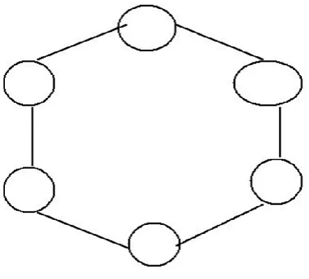
Ring topology: A network topology that is set up in a circular
fashion in which data travels around the ring in one direction and each device on the ring acts as a repeater to keep the signal strong as it travels, shown in figure 8.
Figure 8. Ring Topology
Each device incorporates a receiver for the incoming signal and a transmitter to send the data on to the next device in the ring. The network is dependent on the ability of the signal to travel around the ring. When a device sends data, it must travel through each device on the ring until it reaches its destination. Every node is a critical link. In a ring topology, there is no server computer present; all nodes work as a server and repeat the signal. The disadvantage of this topology is that if one node stops working, the entire network is affected or stops working. Switching techniques: When there are many devices, it is necessary to develop suitable mechanism for communication between any two devices. One alternative is to establish point-to-point communication between each pair of devices using mesh topology. However, mesh topology is impractical for large number of devices, because the number of links increases exponentially (n(n-1)/2, where n is the number of devices) with the number of devices. A better alternative is to use switching techniques leading to switched communication network. In the switched network methodology, the network consists of a set
of inter connected nodes, among which information is transmitted from source to destination via different routes, which is controlled by the switching mechanism. The end devices that wish to communicate with each other are called stations. The switching devices are called nodes. Some nodes connect to other nodes and some are to connected to some stations. Key features of a switched communication network are irregular Network Topology, FDM or TDM for node-to-node communication, existence of multiple paths between a source-destination pair for better network reliability, switching nodes are not concerned with the contents of data and their purpose of providing a switching facility that moves data from node to node until they reach the destination. The network is characterized by switching strategy which is used to determine how the data in a message traverses its route. There are two main switching strategies: circuit switching and packet switching, shown in figure 9.
Figure 9. Switching Techniques
Circuit switching reverses a dedicated end to end path from the source to the destination before starting to transmit the data. The path can be real or virtual circuit. After the transmission is done the path should be released. In packet switching routes packets individually in the network, the network resources can be better utilized. The packet typically consists of a header, payload and a tail. The header carries the routing and sequence information. The payload is the actual data to be transmitted. The tail is the end of the packet and typically contains the error checking code. A switch performing stored and forward as shown in figure 10 will wait to forward a frame until it has received the entire frame. Store and forward is most often used in environments supporting reliable physical or data link protocols. A received frame is often checked for errors before being forwarded. This type of switch is inherently slower in environments where upper layer protocols already provide reliable services.
Virtual Cut through switches begin forwarding the frame as same as the switch has read the destination address. A cut through switch will forward the data before it has completed receiving the frames in figure 11. These switches will function at wire speed, forwarding traffic as fast as it receives it all cut through switches have no RAM buffer for storing frames.
Figure 11. Virtual Cut through switching
Wormhole switching for NoC is challenging from NoC application design and switch complexity reduction. Due to its good performance and small buffering requirement, wormhole switching is being considered as a main network flow control mechanism for on chip networks. Wormhole switching allocates buffers and physical channels (PCs) to flits instead of packets. A packet is decomposed into one or more flits. A flit, the smallest unit on which flow control is performed. This results in that the flits of packets are delivered in a pipeline fashion. A packet is segmented into four flits, with one head flit leading two body flits and one tail flit and then the four flits are transmitted in pipeline via switches as shown in figure 12.For the same amount of storage, it achieves lower latency and greater throughput.
Figure 12. Flits delivered in a pipeline
A coding technique that reduces the coupling switching activity by taking the advantage of end-to-end encoding for wormhole switching. There are three encoding schemes: In Scheme I, focus on reducing Type I transitions, In Scheme II, both Types I and II transitions are taken into account for deciding between half and full invert, depending the amount of switching reduction. Finally, In Scheme III, consider the fact that Type I transitions show different behaviors in the case of odd and even inverts and make the inversion which leads to the higher power saving. A Type I transition occurs when one of the lines switches when the other remains unchanged. In a Type II transition, one line switches from low to high while the
other makes transition from high to low .A Type III transition corresponds to the case where both lines switch simultaneously. Finally, in a Type IV transition both lines do not change. A coding technique that reduces the coupling switching activity by taking the advantage of end-to-end encoding for wormhole switching. There are three encoding schemes: In Scheme I, focus on reducing Type I transitions, In Scheme II, both Types I and II transitions are taken into account for deciding between half and full invert, depending the amount of switching reduction. Finally, In Scheme III, consider the fact that Type I transitions show different behaviors in the case of odd and even inverts and make the inversion which leads to the higher power saving. A Type I transition occurs when one of the lines switches when the other remains unchanged. In a Type II transition, one line switches from low to high while the other makes transition from high to low .A Type III transition corresponds to the case where both lines switch simultaneously. Finally, in a Type IV transition both lines do not change. The proposed encoding architecture, which is based on the odd invert condition. Consider a link width of w bits. If no encoding is used, the body flits are grouped in w bits by the NI and are transmitted via the link. In our approach, one bit of the link is used for the inversion bit, which indicates if the flit traversing the link has been inverted or not. More specifically, the NI packs the body flits in w − 1 bits.
The encoding logic E, which is integrated into the NI. The block E is different for the schemes. To make the decision, the previously encoded flit is compared with the current flit being transmitted. This latter, whose w bits are the concatenation of w − 1 payload bits and a “0” bit, represents the first input of the encoder, while the previous encoded flit represents the second input of the encoder .The w − 1 bits of the incoming (previous encoded) body flit are indicated by Xi (Yi ),i = 0, 1, . . . ,w −2. The wth bit of the previously encoded body flit is indicated by inv which shows if it was inverted (inv = 1) or left as it was (inv = 0). In the encoding logic, each Ty block takes the two adjacent bits of the input flits (e.g., X1X 2Y1Y2, X2X3Y2Y3, X3X4Y3Y4, etc.) and sets its output to “1” if any of the transition types of Ty is detected. This means that the odd inverting for this pair of bits leads to the reduction of the link power dissipation. The Ty block may be implemented using a simple circuit. The second stage of the encoder, which is a majority voter block, in which a higher number of 1s in the input of the block compared to 0s. If this condition is satisfied, in the last stage, the inversion is performed on odd bits. The decoder circuit simply inverts the received flit when the inversion bit is high.
dropped when traversing in a topology to the total packets sent by the source nodes in that topology. A topology with a Dropping Probability with a value of ‘0’ suggests that no packets get dropped, 100 would imply that all packets are dropped. Offered Traffic refers to the average amount of traffic generated by each source terminal of the NoC. Generally, the above discussed metrics are calculated with offered traffic as the independent variable. A NoC topology is said to be productive if high throughput and low latency are achieved and it consumes lesser energy and provided smaller area overhead. Furthermore, NoC topologies that have smaller diameter, lesser mean distance, smaller node degree, greater bisection width and lesser connectivity of their routers are preferable. But, these constraints are inter linked and are a trade-off to one another.
RESULT AND CONCLUSION
The proposed encoding scheme whose goal is to reduce power dissipation by minimizing the coupling transition activity on the links of the inter connection network. There are three types of encoding schemes. In scheme I we focus on reducing type I transition while in scheme II both type I and type II transition are taken into account. Finally in scheme III we consider the fact that type I transition show different behavior in case of odd and even inverts. In this paper scheme I is used for reducing the number of type I transition (by converting them to type III and type IV transition) and type II transition (by converting them to type I transition). The scheme decide whether odd inversion or no inversion of the input data lead to the link power dissipation. A type I transition occurs when one of the lines switches while the others stays unchanged. In a type II transition one line switch as from low to high and the other from high to low. A type III transition occurs when both lines switch simultaneously, finally in a type IV transition both lines do not switch. Effort of odd inversion on change of transition type is given in table 1.
Table 1. Effect of Odd inversion
Table 2. Power analysis of existing system
From table 2 and table 3 power analysis was made and it was found that the proposed system takes the total power of 32%. It save the power up to 68% than the existing system.
Table 3. Power analysis of proposed system
Figure 13 shows the Majority voter block result. In result portion the first 16 bits represent previous encoded bits and the second 16bits represent current encoded bits. When the previous bits and current bits are compared, if the transition occur the inversion is performed on odd bits.
Figure 13. Majority voter block result
As technology scales, important new opportunities emerge for VLSI- IC designer. Understanding technology trends and specific application is the main criterion for designing efficient and effective chips. There are several difficult and existing challenges facing the design of complex IC’s. To continue its phenomena historical growth and continue to flow Moore’s law, the semiconductor industry will require advances on all front from front –end process and lithography to design innovative high performance processor architecture and NoC solution over SoC. The proposed encoding schemes are agnostic with respect to underlying NoC architecture in the sense that their application doesn’t require any modification in the router and routers path. The data encoding technique in which number of switching transition in data word, is brought down to reduce the power dissipation. The scheme aimed at reduce the power dissipation by the links of an NoC. In fact links are responsible for a significant fraction of the overall power dissipated by the communication system. The proposed scheme used less number of gates and links. It leads to reduce the power dissipation by the links. The proposed scheme which allows to save power more than 50% over power dissipation.
REFERENCES
Ki, K. W., B. Kwang Hyun , N. Shanbhag, C. L. Liu, and K. M. Sung, 2000. “Coupling-driven signal encoding scheme for low-power interface design”in Proc. IEEE/ACM Int.
Conf. Comput.-Aided Design, Nov. pp. 318-321.
Murali, S., C. Seiculescu, L. Benini, and G. Deicheli, 2009. “Synthesis of networks on chips for 3D systems on chips,”
in Proc. Asia South Pacific Design Autom Conf., Jan.2009,
pp. 242–247.
Nima jafarzadeh, Maurizio Palesi,“Data encoding techniques for reducing energy consumption in Network On Chip,”
IEEE Trans.VLSI system,vol..22,no.3. March 2014.
Palesi, M., G. Ascia, F. Fazzino, and V.Catania, “Data encoding scheme in Networks on chip, ” IEEE Trans.
Computer.-Aided Design Integration cktSyst., vol. 30, no.
5, pp. 774–786, May2011.
Pande, P.P., C. Grecu, M. Jones, S. M. 2005. Andre Ivanov, and R.Saleh,”performance Evaluation and Design Trade-Offs for Network-on-Chip interconnects Arch,” IEEE Trans on Computers, vol. 54, no. 8, pp.1025-1040, August. Srinivasan, K. and K. S. Chatha, 2006. “Layout aware design
of mesh based NoC architecture,” in proc. Int .
Cons.Hardw.Softw. Co-design syst. Synthesis, pp.136-141. Stan, M.R. and W.P. Burieson, “Bus- invert coding for low power I/O,” IEEE Trans.Very Large Scale Integr. (VLSI) Syst. Vol.3. no.1.pp.49-58 Mar.1995.