EFFECT OF BUMP WIDTH ON THE
EFFICIENCY OF HIGH-LOW 4H-SIC
IMPATT AT Ka-BAND WINDOW
FREQUENCY
SOUMEN BANERJEE
Department of Electronics & Communication Engineering, Hooghly Engineering & Technology College Vivekananda Road, Pipulpati, Hooghly-712103, West Bengal, India
http://www.hetc.ac.in
PRIYA CHAKRABARTI
Department of Electronics & Communication Engineering, Institute of Engineering & Management Y-12, Salt Lake Electronics Complex, Sector-V, Kolkata-700091. West Bengal, India
RIYA BAIDYA
Department of Electronics & Communication Engineering, Institute of Engineering & Management Y-12, Salt Lake Electronics Complex, Sector-V, Kolkata-700091. West Bengal, India
Abstract:
The effect of bump width on the efficiency of high-low p+nn-n+ single drift 4H-SiC Impatt diode has
been investigated at Ka-band (35 GHz) window frequency. A drift diffusion model has been used to study the parameters at optimum bias current density. The diode is designed to operate at millimeter wave frequency. The highest efficiency obtained is found to be at and around 25.47% if the high-to-low doping ratio is varied from 1000 to 50 for a fixed n layer width of 0.8 μm. The conversion efficiency is found to be higher at lower bump width for small doping density ratio. As the doping density is increased the peak efficiency is found to shift towards higher bump width.
Keywords: High-low single drift Impatt Diode; Bump width; Ka-Band; 4H-Silicon Carbide.
1. Introduction
The electromagnetic spectrum ranging from 26.5-40 GHz is designated as the Ka-band. Worldwide research is going on Ka-band; particularly at 35 GHz window frequency where the atmospheric attenuation is found to be relatively low [Gasiewski, (2000)]. The importance of 35 GHz atmospheric window frequency lies in its wide application in the fields of communication satellites and high resolution, close-range targeting radars aboard military airplanes. Moreover some frequencies of Ka-band are used for vehicle speed detection by law enforcement and the Kepler Mission uses this frequency range to downlink the scientific data collected by space telescope. Apart from the conventional uses, systems based on millimeter wave offers many advantages such as smaller size, lighter weight high accuracy and resolution, improved signal penetration through cloud, smoke and dust and reduction in antenna size. It is therefore clear that millimeter wave technology is on the verge of significant growth. To cope with this development researchers are trying to develop solid state sources capable of delivering high power at Ka-band. Fortunately Impatt Diodes provide the perfect solution in being the most powerful solid state source among the commercially available ones. These Avalanche Transit Time Diodes are capable of generating high power at microwave, millimeter & sub-millimeter wave thereby covering a wide range of frequency spectrum. These diodes are employed as solid state transmitters in tracking radars, radio meters, missile seekers and in various civilian and space communication systems.
high frequency applications. The peak power capability of SiC based Impatt is expected to be at least two orders of magnitude higher than the existing Si and GaAs Impatt Diodes.
Among all the polytypes of SiC, the availability of good quality single crystal wafers of α-SiC makes them the most suitable material for electronic devices. Recent achievements in growth processing & characterization of 4H-SiC have enhanced their commercial availability [Madar, (2006)]. The growth of thick and controlled doped layers on 4H-SiC are possible owing to the development of VLS (Vapour-Liquid-Solid) growth technique [Yakimova and Janzen, (2000)].
The formation of low resistance ohmic contacts to p-doped 4H-SiC has recently been resolved to a certain extent. Using alloy composition such as Ni/Al to p-SiC, a contact resistivity of the order of 10-6 cm2 can
be practically realized [Vang, et al., (2006)]. 4H-SiC has higher carrier mobility as compared to 6H-SiC.
In recent years, scientists around the globe are carrying out continuous research activities on 4H-SiC based electronic devices. 4H-SiC based single drift Impatt exhibiting microwave oscillations have already been experimentally demonstrated at X-band [Vassilevski, (2001)]. Fabrication of 4H-SiC high-low SDR Impatt has already been carried out [Yuan. et. al., (2001)] yielding 1mW RF power at 7.75 GHz. Many more theoretical
and experimental studies on Impatts based on 4H-SiC have recently been reported [Khan and Cooper, (2000)], [Ono, et. al., (2005)], [Zhao, (2000)], [Mukherjee, et. al., (2008)], [Jeong, et. al., (2002)], [Mukhopadhyay, et. al., (2007)], [Zhao, (2006)].
In the present paper the authors have considered the performance of high-low SDR p+nn-n+ structure of
4H-SiC based Impatt Diode at 35 GHz window frequency. The properties are studied taking into consideration the effect of mobile space charge at optimum bias current density. The entire paper is aimed at revealing the role of bump width in improving the millimeter wave performance of 4H-SiC Impatt Diode.
2. Simulation Methodologies
2.1. Material parameters, design parameters and doping profile
In the simulation scheme of DC analysis of Impatt diode, the values of the material parameters of 4H-SiC are taken from the reported results published in referred journals and electronic archive
[www.ioffe.ru/SVA/NSM/Semicond]. Some notable material parameters of 4H-SiC are enlisted in Table-1 and the
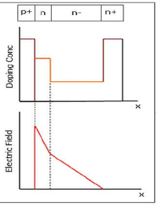
design parameters are shown in Table-2. The doping profile and electric field profile of high-low SDR 4H-SiC Impatt diode is shown in Figure-1. The operating frequency of Impatt diode essentially depends on the transit time of charge carriers to cross the depletion layer of the diode. Single Drift Region (SDR) structure of Impatt diode are designed and optimized through a generalized double-iterative simulation scheme based on drift-diffusion model used for analysis of Impatt action. Computer simulation is carried out at an operating frequency of 35 GHz and the width of the epilayers are accordingly chosen using the transit time formula [Sze and Ryder, (1971)] W = 0.35 vsn/f; where W, vsn and f are the total depletion layer width, saturation velocity of electrons and
Figure – 1. Doping profile and Electric Field profile of p+nn-n+ Single drift Impatt diode
2.2. Computer Simulation Techniques
The following assumptions are made in the computer analysis of single drift Impatt diode; (a) One dimensional model of the p-n junction is treated; (b) The electron and hole velocities are taken to be saturated and independent of the electric field throughout the space charge layer.
The computer simulation method starts with DC analysis described in details elsewhere [Pati, et. al., (1989)],
[Banerjee, et. al., (1985)], [Roy, et. al., (1979)]. In this method the computation starts from the field maximum
near the metallurgical junction. The distribution of DC electric field and carrier currents in the depletion layer is obtained by the double - iterative computer method, which involves iteration over the magnitude of field maximum (Em) and its location in the depletion layer. A computer algorithm has been developed for
simultaneous numerical solution of Poisson’s equation, carrier continuity equations and the space charge equation taking into account the effect of mobile space charge and carrier diffusion in order to obtain the electric field profiles and carrier current profiles. Avalanche breakdown occurs in the junction when the electric field is large enough such that the charge multiplication factors become infinite. The depletion layer of an Impatt diode is commonly divided in to a high-field avalanche region of width WA and low-field drift region of width WD.
The avalanche zone width is customarily defined as the region where 95 % of the impact ionization takes place. The breakdown voltage is calculated by integrating the spatial field profile over the total depletion layer width. Large number of charge carriers emerges from the avalanche zone and interacts with the field while crossing the drift zone. This interaction leads to the generation of high frequency oscillations. The necessary device equations have been simultaneously solved satisfying the appropriate boundary conditions. The DC-to-Millimeter wave conversion efficiency is calculated from the approximate formula [Scharfetter and Gummel, (1969)] (%) = (1xVD) / ( x VB); where VD = Voltage drop across the drift region and VB = Breakdown
voltage.
Table 1. Material parameters of 4H-SiC
Parameters 4H-SiC
Band gap energy, Eg (eV) 3.26
Thermal Conductivity (W/cm K) 4.9
Hole saturation velocity, vsp (105 ms-1) 2.2
Maximum Efficiency (%) 25.47
Table 3 : Peak efficiency for different doping density ratio For High-Low SDR Impatts
Doping density ratio Bump width (m) Peak efficiency (%)
1000 0.81 25.47
300 0.81 25.46
100 0.80 25.48
50 0.80 25.45
10 0.75 25.40
5 0.69 25.01
2 0.60 24.04
3. Results and Discussions
The material parameters of 4H-SiC and its structural parameters at the designed frequency of 35 GHz are enlisted in Table 1 and 2 respectively. Considering the optimized bias current density of 0.44 x 10⁸ A/m2, the
simulated parameters obtained are shown in Table 2.
Figure 2 shows the plot of Electric Field Profile for High-Low SDR Impatt Diode with doping density of 6.8 x 10²² m-3; doping density ratio of 10 and total depletion layer width of 2.3 μm. The figure reveals that the
Figure 2 : Electric field Profile of High-Low SDR diode at doping density of 6.81022 m-3 and doping density ratio of 10.
Figure 3 : DC to millimeter wave conversion efficiency vs bump width of High-Low SDR diode for different doping density ratio
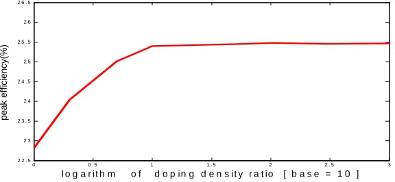
Figure 4 : Peak efficiency vs Log (doping density ratio) for High-Low SDR Impatt diode
4. Conclusion
The Impatt diode based on 4H-SiC generates millimetre wave frequencies with high conversion efficiency. The maximum DC-to-Millimeter wave conversion efficiency for high-low single drift 4H-SiC Impatt is found to be 25.47%. From this simulation study it is quite evident that the conversion efficiency is higher at lower bump width for small doping density ratio, however the peak efficiency falls. Hence a small doping density ratio is
0 . 4 0 . 5 0 . 6 0 . 7 0 . 8 0 . 9 1 1 . 1 1 . 2 1 . 3 1 . 4
1 0 1 2 1 4 1 6 1 8 2 0 2 2 2 4 2 6
w id t h o f h i g h e r d o p e d re g io n (m i c ro m e t e r)
E
ff
ici
en
cy(
%) d a ta 1
d a ta 2
d a ta 3
d a ta 4
d a ta 5
d a ta 6
d a ta 7
d o p i n g d e n s i ty ra ti o
1 0 0 0 3 0 0 1 0 0 5 0 1 0 5 2
0 0 . 5 1 1 . 5 2 2 . 5 3
2 2 . 5 2 3 2 3 . 5 2 4 2 4 . 5 2 5 2 5 . 5 2 6 2 6 . 5
l o g a r it h m o f d o p in g d e n s it y r a t io [ b a s e = 1 0 ]
[6] Vang H, et al. (2006): Ni-Al ohmic contact to p-type 4H-SiC. Superlattices and Microstructures, 40, pp. 626-631.
[7] Vassilevski K. V.; Zorenko A. V.; Zekentes K. (2001): Experimental observation of microwave oscillations produced by pulsed
Silicon Carbide Impatt diode. Electronics Letters, 37(7), pp. 466-467.
[8] Yuan L., et al. (2001): Experimental demonstration of a Silicon Carbide Impatt Oscillator. IEEE ED Letters, 22(6).
[9] Khan I. A.; Cooper J. A. (2000): Measurement of high field electron transport in Silicon Carbide. IEEE ED, 47(2).
[10] Ono S.; Arai M.; Kimura C. (2005): Demonstration of high power X-band oscillation in p+nn+ 4H-SiC IMPATT diodes with guard-ring
termination. Materials Science Forum, 981-4, pp 483-485.
[11] Zhao J. H. (2000): Monte Carlo Simulation of 4H-SiC IMPATT diode. Semicond. Sci. Technol., 15, pp. 1093-1100.
[12] Mukherjee M.; Mazumder N.; Dasgupta A. (2008): Simulation experiment on optical modulation of 4H-SiC mm-wave high power
IMPATT oscillator. Jr. of European Microwave Association (UK), 4, pp 276-82.
[13] Jeong J. K.; Hwang C. S.; Kim H. J. (2002): Low temperature 4H-SiC epitaxial growth on 4H-SiC (1120) and (1100) faces by
Organometallic Chemical Vapour Deposition. Journal of the Electrochemical Society, 149, pp. 6526-6531.
[14] Mukhopadhyay S., et al. (2007): Mobile Space Charge Effect in 4H-SiC IMPATT Diodes. Proc. of XIVth International Workshop on
the Physics of Semiconductor Devices (IWPSD-2007), TIFR & IIT Mumbai, India, pp. 268-272.
[15] Zhao W. (2006): Epitaxial growth of SiC films at low temperature and its photoluminescence. 8th International Conf. on Solid State
and Integrated Circuit Technology, pp 932-934.
[16] Electronic Archive: www.ioffe.ru/SVA/NSM/Semicond.
[17] Sze S. M.; Ryder R. M. (1971) : Microwave Avalanche Diodes. Proc. IEEE Special Issue on Microwave Semiconductor Devices.
[18] Pati S. P.; Banerjee J. P.; Roy S. K. (1989): The distribution of negative resistivity in the active layer of Millimeter wave double drift
region diodes. J. Appl. Physics, 22, pp. 959-964.
[19] Banerjee J. P.; Pati S. P.; Roy S. K. (1985): A Computer analysis of the distribution of high frequency negative resistance in the
depletion layer of IMPATT Diodes. Proc. of Numerical Analysis of Semiconductor Devices and Integrated Circuits (NASECODE IV), Dublin, Ireland, pp. 494-498.
[20] Roy S. K.; Sridharan M.; Ghosh R.; Pal B. B. (1979): Computer method of the DC field and carrier current profiles in the Impatt
devices starting from the field extremum in the depletion layer. Proc. of Numerical Analysis of Semiconductor Devices and Integrated Circuits (NASECODE I), Dublin, Ireland, pp. 226.