e-ISSN: 2278-067X, p-ISSN: 2278-800X, www.ijerd.com
Volume 6, Issue 8 (April 2013), PP. 46-52
Data Acquisition System Using Master – Slave
Communication through ATmega32A Microcontroller
Yadav Raghvendra Satyanarayan
1, Yadav Satyendra Satyanarayan
2 1, 2 M.Tech, Instrumentation & Control Engineering,Faculty of Technology Dharmsinh Desai University, Nadiad, Gujarat, India
Abstract:- This paper presents a data acquisition system using master – slave communication using ATmega32A microcontroller. In this system, we can do the analog to digital conversion using slave microcontrollers. Then by using SPI (Serial Peripheral Interface) protocol we can get that slave microcontrollers data to the master microcontroller and save that analog to digital convertor data to the master microcontroller memory. We can use those data for further processing.
Keywords:- ATmega32A microcontroller, Data Acquisition System, Analog to Digital Converter,
Master – Slave Communication, SPI (Serial Peripheral Interface) Protocol,
I.
INTRODUCTION
As we know that this project is based on the data acquisition system so, it is necessary to understand the data acquisition system first.[6] In data acquisition system there are number of stages involved as shown below:
Fig.1: Block diagram of Data Acquisition System
Each stages of this Data Acquisition system described below:
A. Sensor
Sensor is a device which provides a usable output in response to a specified measurand. [1]
B. Signal Conditioning
This is a stage of data acquisition system which converts the analog signal coming from the sensors into appropriate range of analog signal which is used for the analog to digital converter.
C. Analog Multiplexer
Multiplexer selects one of channel of analog signal from multiple analog signal channels.
E. Program Sequencer
This controls the timing of the selection of analog channel of multiplexer and timing of sample – hold circuit and maintaining the perfect synchronization between these two circuits.
F. Analog to Digital Converter
This converts the analog signal into digital form.
I have used ATmega32A (AVR Family) microcontroller because it have in-built analog to digital converter and it also supports the SPI protocol for communication. In SPI protocol, when the communication will establish between two microcontrollers at that time one will work as master microcontroller and second as slave microcontroller. In the microcontroller we can easily select one microcontroller as master and other as slave microcontroller. SPI (Serial Peripheral Interface) is a synchronous serial data link that operates in full duplex mode. SPI is four pins communication protocol which are MISO (Master In Slave Out), MOSI (Master Out Slave In), SCK (Serial Clock) and SS (Slave Select) pins. [3]
We can add maximum 26 no. Of slaves for single master, but the circuitry becomes more complex so we can use fewer slaves to communicate with the master microcontroller. The selection of slave is done by the master by simply pull down (at zero voltage level) the pin PB4 (Active low “Slave Select” pin of ATmega32A) of slave microcontroller. Each microcontroller has eight channel in-built analog to digital converter. Every slave microcontrollers continuously do the analog to digital conversion of analog signals of different sensors. Sensors includes such as temperature sensor, pressure sensor, motion sensor, displacement sensor or any other sensors. Then each slave will store the A/D data into their individual memory. Then from the request of master the slave will send that data using SPI protocol to the master.
II.
HARDWARE
We have used ATmega32A microcontroller. It has advanced RISC (Reduced Instruction Set Computing) architecture. It has 131 single cycle execution instructions. It has 32 KB of flash program memory, 1024 bytes EEPROM and 2 KB of SRAM. It has eight channel 10-bit ADC (Analog to Digital Converter) and SPI interface for communication. The SFR’s (Special Function Register) related for the in-built ADC and SPI are explained below:
A. ADC related SFR’s
The ADC related SFR’s are listed below: [4]
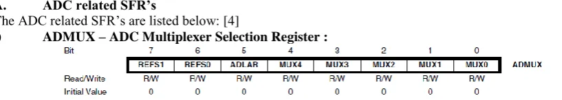
i) ADMUX – ADC Multiplexer Selection Register :
Bit 7:6 – REFS1:0 (Reference Selection) Bits: Select the voltage reference for the ADC, as shown in table. If
these bits are changed during a conversion, the change will not go in effect until this conversion is complete (ADIF in ADCSRA is set).
TABLE I Voltage Reference Selections for ADC
REFS1 REFS0 Voltage Reference Selection
0 0 Aref, Internal Vref turned off
0 1 AVCC with external capacitor at Aref pin
1 0 Reserved
1 1 Internal 2.56V Voltage Reference at Aref pin
Bit 5 – ADLAR (ADC Left Adjust Result): This bit affects the presentation of the ADC conversion result in
the ADC Data Register. Write one to ADLAR to left adjust the result. Otherwise, the result is right adjusted.
Bits 4:0 – MUX4:0 (Analog Channel and Gain Selection Bits): The value of these bits selects, which
combination of analog inputs are connected to the ADC. These bits also select the gain for the differential channels. If these bits are changed during a conversion, the change will not go in effect until this conversion is complete (ADIF in ADCSRA is set).
Bit 7 – ADEN (ADC Enable): Writing this bit to one enables the ADC. By writing it to zero, the ADC is turned off. Turning the ADC off while a conversion is in progress will terminate this conversion.
Bit 6 – ADSC (ADC Start Conversion): In Single Conversion mode, write this bit to one to start each
conversion. In Free Running Mode, write this bit to one to start the first conversion. ADSC will read as one as long as a conversion is in progress. When the conversion is complete, it returns to zero. Writing zero to this bit has no effect.
Bit 5 – ADATE (ADC Auto Trigger Enable): When this bit is written to one, Auto Triggering of the ADC is
enabled.
Bit 4 – ADIF (ADC Interrupt Flag): This bit is set when an ADC conversion completes and the Data
Registers are updated. The ADC Conversion Complete Interrupt is executed if the ADIE bit and the I-bit in SREG are set.
Bit 3 – ADIE (ADC Interrupt Enable): When this bit is written to one, the ADC Conversion Complete
Interrupt is activated.
Bits 2:0 – ADPS2:0 (ADC Pre-scalar Select Bits): These bits determine the division factor between the XTAL
frequency and the input clock to the ADC.
iii) ADCL and ADCH – The ADC Data Register
iv) SFIOR – Special Function IO Register :
Bit 7:5 – ADTS2:0 (ADC Auto Trigger Source): If ADATE in ADCSRA is written to one, the value of these
bits selects which source will trigger an ADC conversion. If ADATE is cleared, the ADTS2:0 settings will have no effect. A conversion will be triggered by the rising edge of the selected Interrupt Flag. Note that switching from a trigger source that is cleared to a trigger source that is set will generate a positive edge on the trigger signal.
B. SPI related SFR’s
The SPI related SFR’s are listed below: [5]
i) SPDR – SPI Data Register:
The SPI Data Register is a read/write register used for data transfer between the Register File and the SPI Shift Register. Writing to the register initiates data transmission. Reading the register causes the Shift Register Receive buffer to be read.
ii) SPCR - SPI Control Register:
Bit 7 – SPIE (SPI Interrupt Enable): This bit causes the SPI interrupt to be executed if SPIF bit in the SPSR
Register is set and if the global interrupt enable bit in SREG is set.
Bit 6 – SPE (SPI Enable): When the SPE bit is written to one, the SPI is enabled. This bit must be set to enable
any SPI operations.
Bit 5 – DORD (Data Order): When the DORD bit is written to one, the LSB of the data word is transmitted
first. When the DORD bit is written to zero, the MSB of the data word is transmitted first.
Bit 4 – MSTR (Master/Slave Select): This bit selects Master SPI mode when written to one and Slave SPI mode when written logic zero. If SS is configured as an input and is driven low while MSTR is set, MSTR will be cleared, and SPIF in SPSR will become set. The user will then have to set MSTR to re-enable SPI Master mode.
Bit 3 – CPOL (Clock Polarity): When this bit is written to one, SCK is high when idle. When CPOL is written
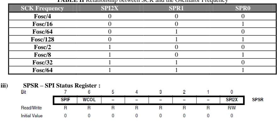
Oscillator Clock frequency “fosc” is shown in the TABLE II. This SPI clock is also controlled by another bit of SPSR (SPI Status Register) which controls the speed of the SPI. That bit named as SPI2X, which increase the SPI speed doubles.
TABLE II Relationship between SCK and the Oscillator Frequency
SCK Frequency SPI2X SPR1 SPR0
Fosc/4 0 0 0
Fosc/16 0 0 1
Fosc/64 0 1 0
Fosc/128 0 1 1
Fosc/2 1 0 0
Fosc/8 1 0 1
Fosc/32 1 1 0
Fosc/64 1 1 1
iii) SPSR – SPI Status Register :
Bit 7 – SPIF (SPI Interrupt Flag): When a serial transfer is complete, the SPIF Flag is set. An interrupt is generated if SPIE in SPCR is set and global interrupts are enabled. If SS is an input and is driven low when the SPI is in Master mode, this will also set the SPIF Flag. SPIF is cleared by hardware when executing the corresponding interrupt handling vector. Alternatively, the SPIF bit is cleared by first reading the SPI Status Register with SPIF set, then accessing the SPI Data Register (SPDR).
Bit 6 – WCOL (Write Collision Flag): The WCOL bit is set if the SPI Data Register (SPDR) is written during
a data transfer. The WCOL bit (and the SPIF bit) is cleared by first reading the SPI Status Register with WCOL set, and then accessing the SPI Data Register.
Bit 5:1 – Reserved Bits: These bits are reserved bits in the ATmega32A and will always read as zero.
Bit 0 – SPI2X (Double SPI Speed Bit): When this bit is written logic one the SPI speed (SCK Frequency) will
be doubled when the SPI is in Master mode (see Table II). This means that the minimum SCK period will be two CPU clock periods. When the SPI is configured as Slave, the SPI is only guaranteed to work at fosc/4 or lower.
III.
SYSTEM
DEVELOPMENT
As we have already discussed that using SPI protocol this system has been developed. From the block diagram of system we can understand that what is happening in the system. As shown in figure the master as well as slave we have used same chip ATmega32A microcontroller. In this system we have used only two slaves which are doing the ADC of analog signals and then transfer that ADC data to the master using SPI protocol. In this system we have used LCD for display of A/D converted data. We can also use the RS232 communication using USART communication between master and a PC and we can directly log the data to the PC and we can store it also. We can also connect the master with other interfaces IC’s using SPI protocol such as external ADC IC’s such as MCP3202, DS1307 real time clock IC etc. For this we have developed PCB for this project. In which, single PCB can use as master as well as slave also. Means a single design of PCB we can use for both master as well as slave.
Fig.2: Block diagram of Data Acquisition system using Master-Slave Communication
The above figure is block diagram of the project. As we have already discussed above in this one controller works as master and others are works as slave. From above figure we can say that analog signals are given to the slave’s in-built A/D converter that transfers those data to the master using SPI protocol. For that we must have to do the programming for master as well as for slave microcontroller also. For that, we have used “AVR Studio 4” assembler to do the programming of the microcontrollers. We have used Sunrom’s ICSP (In-Circuit Serial Programmer) for programming of microcontroller.
That programmer is also based on the SPI protocol and according to that it selects a microcontroller as slave and loads the program into microcontroller’s flash memory. This programmer we can use for the most of AVR Family of the Atmel microcontrollers. It is available with the USB connector so we can use it with our laptops easily and anywhere.
For developing of this project we have used as hardwares are ATmega32A microcontroller, ICSP programmer as well as different types of sensors, which are generating electrical signal according to the change in measurand. Basically power supply is basic need of any project so, we have also used the +5V power supply to power up the microcontroller. We have used temperature sensor (LM35) as sensor to get the analog signal according to the temperature of its surrounding area. After developing of system, the next objective is programming and for that the flow chart of programming is necessary.
IV.
FLOW
CHART
Flowchart is the first requirement for developing the programming for any application for any microcontroller. As shown in Fig.3 the flowchart indicates the way or direction of the program. For this project the first requirement is initialization of LCD using program. We can connect the LCD with master or with slave as per our requirement. We have connected the LCD with the master controller. After that we have to select the controller as master or slave, for that we have to write “1” at the bit of “MSTR” of “SPCR” SFR of the controller, for other we will write zero so that controller will selects as slave.
As we have informed above that the programming for master as well as slave are different that we can see from the flowchart of programming. By using programming skills we can easily make a program which is suitable for every slave controller. In that, master will simply polling all slaves one by one to get the ADC data of each slave. At that time each slave other than that slave (which is connected with the master using SPI protocol) will do the A/D conversion and store that A/D conversion data into their individual memory.
Fig.3: Flowchart of programming of Data acquisition System using Master – Slave communication
V.
CONCLUSIONS
REFERENCES
[1]. D. Patranabis, Sensors and Transducers, 2nd Edition, Prentice – Hall of India (PHI) Publication, New Delhi, 2007.
[2]. Ramakant A. Gayakwad, Op-Amps and Linear Integrated Circuits, 4th Edition, Prentice – Hall of India (PHI) Publication, New Delhi,2007.
[3]. Archana Ramesh R, M.S.R.Sekhar, “Design and Verification of Serial Peripheral Interface using OVM”, International Journal of Electronics Communication and Computer Technology (IJECCT), Volume 2, Issue 6 (November 2012), pp. 267-269.
[4]. “Datasheet of ATmega32A Microcontroller”, “Analog to Digital Converter”, www.alldatasheet.com and www.atmel.com, pp.209-227.
[5]. “Datasheet of ATmega32A Microcontroller”, “Serial Peripheral Interface”, www.alldatasheet.com and www.atmel.com, pp.138-146.