Abstract –An ‘I’ shaped slot antenna with finite slotted ground plane is presented. It is a micro-strip feed mechanism based antenna for impedance matching with 50Ω coaxial cable. The antenna geometry is simulated using IE3D simulator. Antenna works well in the frequency range 4.35 GHz to 4.55 GHz. It is basically a light weight, cost effective antenna, which can be used for wireless communication in UWB band. The antenna structure involves comparison of micro-strip line length variation using same ‘I’ shaped slot on the dielectric layer with finite slotted ground plane. Final antenna geometry i.e. with ‘I’ slot on dielectric plane and three horizontal slots on the ground plane, shows better improvement in the radiation characteristics. It can be clearly seen that impedance matching is dependent upon the micro-strip length. Varying the length also results in changes in the inductance and the capacitance value of the antenna structure. Microstrip antenna is with ‘I’ slot and finite ground plane with three horizontal slots, improves properties like resonant frequency, gain, return loss, which may affect the antenna performance. This structure uses single layer configuration; ‘I’ shape slot on the dielectric patch and three rectangular horizontal slots on the finite ground plane. The antenna simulation yields -33.91 dB return loss at 4.538 GHz resonant frequency with 4.49% bandwidth with a size of 36.75x39.7x1.5mm3. The proposed antenna design presents a good choice for compact and low-cost microwave integrated systems.
Index Terms— Rectangular patch, microstrip antenna
(MSA), ultra wideband (UWB), Slot antenna, Return loss (RL), Bandwidth (BW), ‘I’ slot.
1) INTRODUCTION
Ultra wideband (UWB) wireless communication allows high rate data transmissions with low power level have embarked great research interests for wireless communications applications in the 3.1Ghz –10.6Ghz frequency band. High-performance UWB antennas need both good impedance matching and low signal distortion within the relative frequency bands. Microstrip patch antennas are mostly used in wireless and cellular mobile communication systems because of their merits, like compactness, light weight and ease of fabrication and
Manuscript received, Feb, 2017
PG Scholar Poonam Rajput, EC, Oriental College of Technology, Bhopal, India, 9425668173.
Professor Prateek Wankhade, EC, Oriental College of Technology,
LPDAs also have a reasonable gain with a very large bandwidth.
In the design we have presented a single layer microstrip patch antenna configuration. Which consist of „I‟ slot on its dielectric plane and a finite ground plane with a vertically located rectangular slot. Concepts of microstrip patch antenna and slot antenna were successfully used to achieve the required antenna performances. The coaxial feed is used as source for the antenna. In this paper, a compact antenna is simulated with three different configurations. As we know that by implementing slots, bandwidth and return loss characteristics can be improved therefore, the proposed geometry invokes slots on dielectric layer and on the ground layer. The proposed design can effectively reduce the overall size of an antenna. Concept of impedance matching is presented using feed point variation, slot implementation. The proposed geometry is very simple but yet so effective, hence can get better radiation characteristics.
Immense research work is being carried out in the field of microstrip patch antennas. The development in the context of microstrip patch antenna is our focus area. The following review emphasized on comparative study of several research works based on microstrip patch antenna. Keisuke Noguchi et al. presented a new circuit model for E-shaped patch antennas (ESPA shown in fig. 1) using the multi-conductor transmission line mode theory (the modal theory) in [1]. Radiation and transmission line modes generated on the ESPA are described and an equivalent circuit is derived from the modal theory. The equivalent circuit described in detail to achieve wideband and multiband characteristics. For wideband ESPAs, the theoretical maximum bandwidth is derived under VSWR criterion. Dual-band ESPA is also discussed theoretically and the return loss vs frequency characteristic is shown in Fig.1. Fig.1 shows dual band characteristics with the maximum return loss value of -21.4 dB and -24.9 dB at 1.73GHz and 2.40 GHz respectively. Impedance bandwidth value of 4.5 % and 10.5 % is obtained at 0.8445 GHz and 1.825 GHz respectively. In [2] Yujian li and Kwai-man luk designed a novel water dense dielectric patch antenna (DDPA) fed by an L-shaped probe. The operation of the proposed water DDPA is similar to the conventional metallic patch antenna. An L-shaped probe is used excitation of the water DDPA (shown in fig 3). Wide bandwidth can be achieved for the designed antenna by choosing a thick supporting substrate between the water patch and the ground plane. A prototype is fabricated to correctness of the design. An impedance bandwidth of 8%, maximum return loss of -22.45 dB (with water dielectric patch), maximum gain of 7.3 dBi, radiation efficiency up to 70%, and symmetrically unidirectional patterns with low
Micro-strip line feed „I‟ shaped slot Antenna with
finite slotted ground plane for Return Loss
enhancement
proposed water DDPA can be conveniently integrated with the solar cells to realize a dual-function design. Xiao Lei Sun et al. designed and studied a dual-band monopole antenna with a very compact area of only for 2.4/5.2/5.8-GHz WLAN applications in [3]. The antenna consisted of an L – shaped and E - shaped elements having resonances at about 2.44 and 5.5 GHz respectively. In [4] Chih-Yu Huang and En-Zo Yu proposed a coplanar waveguide fed dual-band slot-monopole antenna suitable for WLAN operation. The designed antenna provides two separate impedance bandwidths of 124 MHz (about 5.1% cantered at 2.45 GHz) and 1124 MHz (about 22.4% centered at 5.5 GHz); both the bandwidths are large enough for the required bandwidth of the 2.4 and 5.2/5.8 GHz WLAN bands. The two frequency bands can be tuned separately.
Amit A. Deshmukh and K. P. Ray proposed a new geometry by integrating a half-U-slot and a rectangular slot inside the rectangular microstrip patch antenna in [5]. The proposed antenna design shows better bandwidth enhancement with gain of more than 7 dBi for the entire BW with the broadside radiation pattern. M.Ali et al. presented a wide-band/dual-band packaged antenna for wireless local-area network (WLAN) applications in the 5.15–5.35 GHz and 5.725–5.825 GHz frequency range in [6]. The effects of coupling between the ground plane and antenna were shown. Fabricated antenna dimensions were of 28x9x3 mm3 on FR4 substrate. In [7] D.K.Shrivastava et al. proposed stack configuration of a wideband U-slot loaded rectangular patch and a horizontal slot loaded rectangular patch antenna. The designed antenna performed wideband operation due to its dual resonance nature. The designed antenna configuration has shown bandwidth enhancement. The resonance operation effect depends upon substrate thickness and slot parameters. The impedance bandwidth of 54.6 % is obtained. The half power beamwidth was found to be approximately 68o and radiation pattern was found to be almost constant throughout the entire bandwidth. In [8] Alireza motevasselian et al. presented an effective approach to reduce the size of patch in rectangular microstrip antennas. The approach was based upon inductively loading the patch using a cuboid ridge and the cuboid ridge is included in the transmission line model of the patch antenna. Mahdi moosazadeh et al. proposed a novel microstrip-fed monopole antenna for a triple-band operation in [9]. The proposed antenna consisted of a pair of symmetrical L and U shape slots inside the rectangular patch that enables proper adjusting of the resonant bands. Proposed antenna geometry was simulated and fabricated on FR4 substrate. Designed antenna covers the desired operating bandwidths, gain, and radiation patterns for WLAN (2.4/5.2/5.8 GHz) and WiMAX (2.5/3.5/5.5 GHz) applications. The antenna had relatively small dimensions of 15x15x1.6 mm3. In [10] Ali Foudazi et al. presented a compact microstrip line fed multi-band monopole antenna. The base of the designed antenna was a diamond-shaped patch that covered the UWB frequency range. For achieving multi-band characteristics, several narrow strips, could be integrated with the antenna. The designed geometry had a substrate size of 16x22x1 mm3 and covers the frequency bands 1.3, 1.8, 2.4 and 3.1–10.6 GHz. which could be used for GPS, GSM, WLAN and UWB applications. The antenna had omnidirectional and stable
radiation patterns across all the relevant bands. A quad-band antenna is simulated using HFSS and fabricated a prototype on FR4 substrate. In [11] Zi-Xian Yang et al. proposed a rectangular patch antenna for bandwidth enhancement, in which polarization could be reconfigured. The antenna had stair-slots on the ground and two p-i-n diodes were used for switching the antenna‟s polarization (linear polarization, left-hand circular polarization and right-hand circular polarization). The 3-dB axial-ratio bandwidths and return loss enhancement were achieved. The asymmetrical slotted ground acted as an excitation plane and modes with different resonant frequency to generate CP radiation, and due to the stair-slots, the lower resonant frequency decreased and the higher one increased. Thus, the overall bandwidths were improved. The proposed antenna could be used for wireless local area network (WLAN) in the range of 2.4GHz – 2.5 GHz in wireless communication systems.
In the proposed design, we will investigate the effects of slot implementation and impedance matching by varying length of micro-strip feed line with a constant feed point. In this paper, the configuration of proposed antenna consist of „I‟ slot on dielectric plane and slotted ground is described in detail in further chapter. Design parameters are discussed, by considering the effects of different dimensions on antenna performances. The proposed antennas as described in Fig. 1 is Simulated with the IE3D version 9.0, and the work is finally concluded.
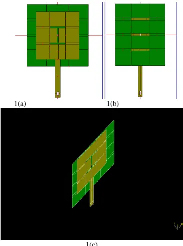
2) ANTENNA DESIGN CONSIDERATION The configuration of single layer microstrip antenna, which consist of „I‟ slot on its radiating patch and a slotted finite ground plane (with three horizontal slots), then variation of length of feed line is considered and the comparative analysis is shown with the different lengths of feed line. First of all an „I‟ shaped slot is designed of 9.46x0.946 mm2
size at the centre of the dielectric patch and on ground plane a vertically located slot of 13.51x1.351 mm2 is designed. The whole geometry is located at the centre (i.e. xf =0 mm, yf =0 mm). The feeding technique used in the design is microstrip line feed. Feed point is calculated as (xf =0 mm, yf =-37 mm). The simulated geometry is shown in Fig.1. Dielectric layer and ground plane dimensions are given in table.1. The substrate is chosen to be FR4 having dielectric constant Ԑr = 4.3 with the height h=1.5 mm. and loss tangent as 0.019. The location of the feed point is obtained from the equation given below;
Xf = reff
L
2 ε
and Yf =W
2
For the patch designing certain calculations have been done with the help of following equations;
Width and Length of patch is given by;
0 r r
V
2
W =
2*f
ε +1
, 0 eff r reffV
L =
2*f
ε
1(a) 1(b)
1(c)
Fig. 1 Antenna 1, 1(a) Top view of antenna, 1(b) Bottom view of antenna, 1(C) 3d view of antenna
The return loss characteristic is shown in figure.2. It shows that antenna 1 initially does not radiate due to its impedance mismatching.
Fig.2. Return loss vs frequency plot
Table.1. Dimensions of antenna (All dimensions are in mm.)
L (length of dielectric plane) 25.75
W(width of dielectric plane) 30.7
Lg (length of ground plane) 36.75
Wg (width of ground plane) 39.7
Ls (length of slot) 9.46
Ws (width of slot ) 0.946
Effective dielectric constant is given by;
r r reff
ε +1 ε -1
1
ε =
+
*
2
2
12h
1+
w
Practical approximate relation for normalized extension of length;
refff refffW
ε
+0.3
+0.264
ΔL
h
=0.412
W
h
ε
-0.258
+0.8
h
Actual length of the patch is given by; eff
L =L+2ΔL
The VSWR vs frequency plot is shown in figure 3. Plot defines that the overall geometry has good radiation properties and good impedance matching at 4.538 GHz.
Fig. 3. VSWR vs frequency plot
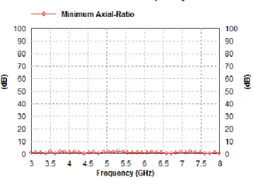
The axial ratio vs frequency plot is shown in figure 4. Plot shows that designed geometry is linearly polarized.
Fig. 4 Axial ratio vs frequency plot
Whole geometry is simulated using FR4 substrate parameters such as; dielectric constant Ԑr = 4.3, height h=1.5 mm. and loss tangent as 0.019. All the dimensions of length variation in micro-strip feed line and the relative results are given in table.3. Outcomes of length of the micro-strip feed line are given in the comparative graph. On comparing all the three plots in figure 5, we come know that result with the length of 2.975 mm (length of micro-strip feed line) is far better, in comparison with the other length variation. It is very clear that impedance matching is totally dependent on the dimensions of the micro-strip feed line. Antenna 3 is simulated with the 1.5 mm thick FR4 substrate having dielectric constant Ԑr = 4.3 and 0.019 loss tangent. Simulation result shows that impedance is perfectly matched and hence antenna 3 starts radiating at 4.2 GHz resonant frequency. All the dimensions for the designing of antenna 3 are tabulated in Table. 3. Designed antenna works in the range of 4.35 GHz to 4.55 GHz. Designed antenna works in c band. As c band is allocated for commercial satellite communications and full time satellite TV networks or raw satellites. So the proposed antenna is a good candidate and can be used easily.
Table.3. dimensions of antenna 3 (All dimensions are in mm.) Size of Geometry Length of Microstrip feed line Width of Microstrip feed line Return loss (RL) 28 MB 2.975 mm λ/2 -33.91 dB 28 MB 3.975 mm λ/2 -14.02 dB 54 MB 4.975 mm λ/2 -10.32 dB
The geometry is simulated using IE3D simulation tool within 3 GHz to 8 GHz operating frequency range. Designed antenna can be used for c band. The comparison on varying length of micro-strip feed line is shown in fig.5. It shows that impedance matching can be done easily using slot implementation, simultaneously it shows that impedance, inductance value is significantly affected by changing the dimensions of the micro-strip feed line. Improvement of overall performance of the design can also be achieved using the concept. Also the finite ground plane acts as a perfect reflector. So that can get maximum radiations in one direction.
Fig. 5 comparative graph with different lengths of micro-strip feed line (L=2.975,L=3.975 and L=4.975)
3) CONCLUSION
In this paper Single layer „I‟ shaped micro-strip slot Antenna with slotted ground (three horizontal slots) is presented. Micro-strip line feeding is used in this structure as a feeding mechanism. Slot implementation is very easy and effective approach for achieving size reduction and for the good performance at the demonstrated frequency relatively. By introducing a finite slotted ground plane impedance matching can be achieved, so that we can have better return loss and hence bandwidth. It is investigated how the micro-strip feed dimensions influence the input impedance. The losses of dielectric substrate were also considered. Simulation results show that design antenna is a good candidate for c band in the range of 4.35 GHz to 4.55 GHz.
REFERENCES
[1] U. Chakraborty et al. “Compact Dual-Band Microstrip Antenna for
IEEE 802.11a WLAN Application” IEEE Antennas and Wireless Propogation Letters, VOL. 13, 2014, pp: 407-410.
[2] Jigar M. Patel et al. “Comparative Analysis of S-Shaped Multiband
Microstrip Patch Antenna” International Journal of Advanced Research in Electrical, Electronics and Instrumentation Engineering Vol. 2, Issue 7, July 2013, pp: 3273-3280.
[3] Xiao Lei Sun et al. “Dual-Band Antenna with Compact Radiator for
2.4/5.2/5.8 GHz WLAN Applications” IEEE Antennas and Wireless Propogation, Vol. 60, issue 12, December 2012.
[4] Chih-Yu Huang and En-Zo Yu “A Slot-Monopole Antenna for
Dual-Band WLAN Applications” IEEE Antennas and Wireless Propogation Letters, Vol. 10, 2011.
[5] Amit A. Deshmukh and K.P.Ray “Compact Broadband Slotted
Rectangular Microstrip Antenna” IEEE Antennas and Wireless Propogation Letters, Vol.8, 2009.
[6] M. Ali et al. “Wide-Band/Dual-Band Packaged Antenna for 5–6 GHz
WLAN Application” IEEE Antennas and Wireless Propogation, Vol. 52, Issue 2, February 2004.
[7] D.K. Srivastava et al. “Wideband electromagnetically coupled
coaxial probe fed slot loaded stacked patch antenna” International Journal of Engineering, Science and Technology, Vol. 3, No. 3, 2011, pp. 154-159.
[8] Alireza Motevasselian et al. “Patch size reduction of rectangular
microstrip antennas by means of a cuboid ridge” IET Microwaves, Antennas & Propagation, Vol. 9, Iss. 15, 2015,pp. 1727–1732. [9] Mahdi Moosazadeh et al. “Compact and Small Planar Monopole
Antenna With ymmetrical L- and U-Shaped Slots for WLAN/WiMAX Applications” IEEE ANTENNAS AND WIRELESS PROPAGATION LETTERS, VOL. 13, 2014, pp. 388-391.
[10] Ali Foudazi et al. “Small UWB Planar Monopole Antenna With Added GPS/GSM/WLAN Bands” IEEE TRANSACTIONS ON ANTENNAS AND PROPAGATION, VOL. 60, NO. 6, JUNE 2012, pp. 2987-2992.
[11] Zi-Xian Yang et al. “Bandwidth Enhancement of a Polarization-
Reconfigurable Patch Antenna With Stair-Slots on the Ground” IEEE ANTENNAS AND WIRELESS PROPAGATION LETTERS, VOL. 13, 2014, pp. 579-582.
Poonam Rajput received her B.Tech. Degree in electronics &
communication from Rajiv Gandhi Proudyogiki Vishwavidhyalaya, Bhopal, (M.P.), and pursuing her M.Tech in electronics and communiation from Oriental College of Technology, RGPV, Bhopal (M.P.), India.
Prateek Wankhade received his B.Tech. Degree from Rajiv Gandhi
Proudyogiki Vishwavidhyalaya, Bhopal, (M.P.), M.Tech Degree in Digital Communication from Rajiv Gandhi Proudyogiki Vishwavidhyalaya, Bhopal, (M.P.). He is an Associate Professor in the Department of Electronics and Communication Engineering, Oriental College of Technology, Bhopal, (M.P.), India.