Practical Design Guidelines for Flex
CHAPTER
5
I
NTRODUCTIONFlexible circuits are obviously unique among electronic packaging technologies in that they off er a wide variety of advantages unobtainable using conventional rigid interconnection technologies. Freeform integration of electronic elements through all three dimensions of space is highly liberating to the design process.
Such advantages, however, cannot be garnered without a thorough understanding of basic fl ex circuit design principles. Proper use of those design principles can provide a path to early success. In contrast, failure to use good design practices can result in early failure. Th e objective of this chapter is to provide information vital to the successful production of fl exible circuit designs—ones that will consistently perform to user expectations.
D
ESIGNP
RELIMINARIESBefore embarking on a fl ex circuit design, it is important that a holistic overview of the project be taken. In this overview, a circuit designer should attempt to take into account as many of the items discussed in the implementation section as are possible or relevant. Th is act of taking stock of the project will help the designer appreciate the broader perspective of the task, minimizing the possibility that a gross and avoidable error will be carried through the design process.
It is also important that the designer keep in mind that fl exible circuit designs require a balancing of both mechanical and electrical concerns. Th ese two competing concerns, the designer will fi nd, oft en oppose each other’s requirements in a design. It will be the holistic approach that will help the designer thread the needle to make the best possible choice from given alternatives.
USEOF MOCKUPS
Let us reassert here the value of using paper doll mockups. Th is simple practice will help the designer prevent many errors by exposing potential
problems early and will save both time and money.
Some modern CAD systems have demonstrated the ability to execute three dimensional layouts required for fl ex circuit applications, but the physical model will probably always prove of some value in addressing both the ergonomic elements of assembly and the concerns of access should fi eld repair be required.
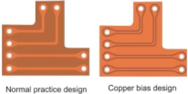
DESIGN WITH A BIAS FOR COPPER
Favoring the use of copper in design is good practice for some very solid reasons, assuming that there are not important confl icts created by the practice. If all other design objectives are met, then the primary reason for maintaining extra copper is that it helps to enhance the dimensional stability of the circuit. Designing with a bias for copper is a practice especially well suited to single-layer fl ex circuit designs. See Figure 5-1.
As indicated before, the decision to add or leave copper should be made in light of the objectives of the circuit’s fi nal use. For example, if a reduction in weight of the fi nal product is a key objective, then there would be need to trade away some of the enhanced dimensional stability. Another reason for maintaining the copper is that it reduces the amount of copper etched and is thus more environmentally friendly in terms of chemical usage.
TOLERANCE SETTING FLEX CIRCUIT DESIGNS
Proper application of tolerances of fl ex circuit design features is a matter that concerns both the fl ex circuit manufacturer and the fl ex circuit user.
Figure 5-1 Designing with a bias for copper improves the circuit’s dimensional stability. It may not be practical for all applications.
Figure 5-2 Copper foil is maintained by design around circuits to provide better panel dimensional stability. Two examples are shown.
In general, it is recommended that the largest practical tolerance be given to all features and locations to
facilitate manufacture. Th is is because the base materials are fl exible and prone to distortion, making accurate measurement over distances diffi cult. To compensate, it is recommended that more than one datum be used on larger circuits. Individual datums
can be provided locally relative to features deemed important. (See Figure 5-3.) Th is will result in a more accurate measurement being taken and can preempt potential confl icts in measurement results between inspectors. To avoid confusion in design, one datum should be defi ned as the primary or master datum and others as secondary or slave datums.
Tight tolerances can be attained, when required, but to do so requires
Figure 5-3 The use of multiple datums, with one being the prime and the others secondary, facilitates both accurate measurement of the circuit and device placement during the assembly process.
*Mil-Std-2118 off ers the following statement regarding tolerances: “Drawing tolerances must refl ect bend and fold allowances between component mounting rigid areas.”
special attention and good techniques. As a result, the expense of tighter tolerance circuits tends to be greater due to anticipated loss of yield. Table 5-1 provides some general guidelines for tolerancing based on diff erent design standards.
Th e values off ered in Table 5-1 are rather generous by today’s standards, however. To provide a global perspective on fl ex circuit feature capability, a 2004 survey of 20 Japanese fl exible circuit manufacturers indicated that more than half of the companies were routinely producing fl ex circuits with traces of 110µm or less, and fi ve companies were producing circuits with features of 70-90µm routinely. Today are a number of fl ex circuit manufacturers in Japan and elsewhere are producing circuits having features of 35 to 50µm and some have shown capabilities down to 25µm and even 10µm feature sizes.
GENERAL GUIDELINESFOR DIMENSIONINGAND TOLERANCING
Proper dimensioning and tolerancing of fl ex circuits is vital to achieving good manufacturing yield. While it is not possible to point out every possible situation where dimensions and tolerances can be used in such a way as to confuse the interpretation of a drawing, there are certain general guidelines that, if followed, can do much to minimize the potential for confusion. Following are a few such guidelines:
•Show suffi cient dimensions so that the intended sizes and shapes can be determined without requiring the distances between features to be calculated (or assumed).
•Provide individual dimensions only once and check them. •State all dimensions clearly so they can only
have a single possible interpretation.
•Show the dimensions between points, lines or surfaces, which have a necessary and specifi c relation to each other or which control the location of other components or mating parts. •Check dimensions to avoid accumulations of tolerances that may permit alternative interpretations.
•Provide dimensions to features, which are shown in profi le making certain that the feature’s dimensions are not ambiguous.
•Do not show dimensions to lines representing hidden surfaces. •Do not use “off part” datums.
SPECIAL DESIGN CONSIDERATIONS
Th ere are some unique elements of fl ex circuit design that require early consideration. Mostly they address mechanical issues that could aff ect usability and/or long term performance. However, they will defi nitely aff ect circuit layout and so are given early consideration.
LAY OUT CIRCUITTO CONSERVE MATERIAL
Conservation of material in fl exible circuit manufacture serves to help keep manufacturing costs down. Th is is important because fl exible circuit materials tend to be expensive in comparison with standard rigid materials such as FR-4.
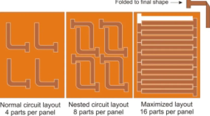
We suggest accomplishing close spacing of the circuit. Th e technique of optimizing the number of circuits per panel is called nesting. Th e term optimizing is used in place of the seemingly more logical term maximizing for a reason, that reason being that the layout of a fl ex circuit should be based on end use, and some uses may demand that portions of the fl ex circuit be properly oriented relative to the grain direction of the foil (such as is required for dynamic fl exing). Th is may result in a less-than-maximum material use for circuit construction. However, when this is not the case, there is the opportunity to lay the circuit out in various ways to get the most out of the material.
Figure 5-4 Proper circuit nesting can greatly improve panel yield and lower overall cost. If folding can be tolerated as an assembly operation, yield can be maximized. For dynamic
fl ex circuit designs, the grain direction requirement may impact layout.
While nesting is routinely performed by the manufacturer, the designer can aid in this process by taking advantage of the fact that fl ex circuits can be bent and folded. Th us, adding a small length to a circuit arm can allow a circuit to be produced more economically, provided the user doesn’t mind adding a folding operation to his assembly process. (See Figure 5-4.) SERVICE LOOPS
Th e addition of a small amount of length to the fl ex circuit beyond the design requirement is advisable for most fl ex circuit applications. Th is little extra length of material is commonly referred to as the service loop length.
Th e purpose of the service loop is off er suffi cient length to facilitate both assembly of the product and servicing of the product once in the fi eld, if it should ever be required. Th e extra length also helps to compensate for small, unforeseen variations in both the package and the fl ex circuit.
Figure 5-5 Staggered length designs facilitate bending of the fl ex circuit; the circuit can only be bent in one direction by design.
STAGGERED LENGTH CIRCUITS (BOOKBINDER CONSTRUCTION)
For ease of fl exing multilayer and rigid fl ex designs, the use of staggered length design is commonly employed. Th e technique is accomplished by adding slightly to the length of each succeeding fl ex layer, moving away from the bend radius. (See Figure 5-5.)
A common rule of thumb is to add length equal to roughly 1.5 times the individual layer thickness. Th is helps defeat whatever tensor strain might have otherwise been built up in the outer metal layers of the multilayer fl ex and prevents buckling of the center of bend layers (see Figure 5-6).
Figure 5-6 Without staggered lengths, layer buckling occurs.
C
ONDUCTORS
IZINGANDR
OUTINGIn general, fl ex circuit conductor width and thickness are determined by a combination of current carrying requirements, the voltage drop allowance and/or characteristic impedance control needs. When designing fl ex circuits for dynamic applications, the use of the thinnest possible copper is recommended. Th us, it is important that the designer opt for wider rather than thicker traces to accommodate basic electrical needs or requirements. Th is practice assures maximum circuit fl exibility.
Table 5-2 can be used to determine maximum current and line resistance for given trace widths with both 35µm (1-oz) and 70µm (2-oz)
copper. Th ese are relatively common foil thicknesses used in much fl ex circuit manufacture, although 18µm (½-oz) and even lower copper foil thicknesses are becoming increasingly important.
A number of diff erent nomographs for determining other electrical values for copper have been developed to simplify copper trace-requirement specifi cation. Th e IPC’s fl ex circuit design specifi cation is a good source for such nomographs for those who have interest. Th ere is an eff ort underway to revise these graphs, which have long been in use, to refl ect more practical values. Conductor Width Maximum Current for 10° C rise 1 oz copper Conductor Resistance milliohms/ft 1 oz copper Maximum Current for 10° C rise 2 oz copper Conductor Rresistance milliohms/ft 2 oz copper 0.005 .25 1280 NA NA 0.010 .6 640 1.0 320 0.015 1.1 400 1.8 200 0.020 1.3 320 2.0 160 0.025 1.5 250 2.5 125 0.030 1.8 200 2.9 100 0.050 2.5 120 4.0 60 0.070 3.2 90 5.0 45 0.100 4.0 60 6.9 30 0.150 5.9 40 9.8 20 0.200 6.9 30 12.0 15 0.250 8.6 25 13.5 12.5
Table 5-2 Current Carrying Capacity of Conductors. Conductor width and copper thickness have a direct impact on the current carrying capacity of a fl exible circuit. The above
table provides a means of determining the conductor width for a 10° C rise
Trace Width Minimums
Th e minimum practical trace width for a fl ex circuit varies from vendor to vendor. Flex circuits with traces 250µm (0.010") and greater are fairly easy to obtain; however, line widths 125µm (0.005") and lower are increasingly common. Flex circuits having features in the range of 50µm (0.002") and lower are available in volume production from a limited number of vendors, but the number of such vendors is growing to keep pace with the demand for ever smaller electronic products.
Th e type of technology used in circuit feature manufacture also heavily infl uences trace width minimums. For example, plated up copper sputtered polyimide base circuits are basically limited in feature size only by the
photolithographic capabilities of the manufacturer. Th us, very small circuit features can be made. For etched circuit traces, however, the trace width and pitch are infl uenced primarily by the thickness of the base copper foil. Typically, the trace pitch limit is nearly linear with copper thickness within a narrow range. 18µm (½-oz) copper will yield circuit features at a 125µm (0.005") pitch, while with 35µm (1-oz) copper, etching becomes more diffi cult under 175µm (0.007") pitch. While some manufacturers can successfully produce 25µm (0.001") features with 18µm copper, vendor capabilities vary widely. It is best to check with the fabricator before attempting to design very fi ne line features.
CONTROLLED IMPEDANCE LINES
Controlled impedance transmission cabling is a popular application for fl ex circuits, and the value of such product is increasing as digital data signaling speeds continue to rise.
Tighter tolerances for etched features are possible with fl ex circuits because of the lower profi le adhesion treatment or “tooth” of the copper. Th e use of thicker fl exible dielectric substrates, if the design allows, can ease somewhat the etching challenge because thicker substrates allow for wider signal lines, which can be fabricated more easily to meet the tight tolerances needed for controlled impedance circuits. Th is topic will be discussed in more detail later in this chapter.
ETCH FACTORS
An etch factor is a tool used by the manufacturer to compensate for isotropic etching process eff ects. It is recommended that the designer check with the vendor to determine if they want inclusion of an etch factor. Usually it is best if the manufacturer makes this adjustment, as they will be most familiar with their process and its capability.
Th e typical line width loss (measured at the top of the trace) due to the etching process is approximately 2x copper foil thickness, although copper type, conductor pitch, etch mask, process chemistry and equipment can all infl uence the results.
CONDUCTOR ROUTING CONCERNS
Th ere are a few general issues related to conductor routing of a fl ex circuit. Th e fi rst item of concern is keeping to a minimum the number of crossovers in the layout. Th is will help to keep the layer count down and lower the cost. Newer CAD systems can respond to such a requirement, but the results may need to be massaged or optimized to make certain that the smallest possible area has been consumed in the process.
Routing of conductors on a fl exible circuit perpendicular to bend and fold is the recommended design practice. Th e purpose is to facilitate the bending or folding process and to minimize stress through the area. In addition, circuitry should be routed on a single copper layer through bend and fold areas whenever possible.
Figure 5-8 Routing options for fl ex circuit trace corners. Avoid sharp corners if possible. A radius is best as it provides a smooth transition and mitigates potential issues related to stress risers.
It is also recommended that designs avoid having right or acute angles (≤ 90°) in circuit routing. Th is is because they tend to trap solution and may over etch in process. Th ey are also more diffi cult to clean aft er processing, so best practice dictates that corners should be provided with a radius if possible. Th e radius also improves signal propagation, as the refl ections at turns are reduced.
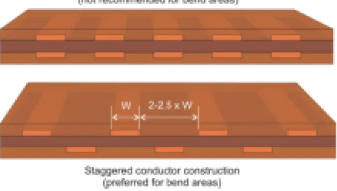
With double-sided fl ex, when and where the conductors must be routed through bend and fold areas and when copper traces are on both sides, the circuit designer should design spaces to be approximately 2-2.5x the trace width.
Preferably, the designer should also stagger traces from side to side. Th e purpose of this practice is to avoid the I-beam eff ect. Th is can be a critical concern in dynamic applications. (See Figure 5-9.)
Figure 5-9 I-Beamed vs. Staggered Conductors. I-beamed constructions increase the stiff ness of the circuit through bend and fold areas. A better alternative, if space allows, is to stagger conductors for improved fl exibility.
Finally, placement of vias within the bend area is highly discouraged as they will adversely aff ect bend formation and create unwanted points of stress and potential crack propagation.
G
ROUNDP
LANED
ESIGNGround areas should be crosshatched if electrical consideration of the design will allow for such. Th e practice helps both to reduce weight and improve circuit fl exibility. Th e size of the openings in the ground plane may be critical depending on the end product requirements for shielding or controlling of characteristic impedance. If openings are too large, some shielding eff ects may be lost, depending on frequency. Also, ground connections for components should be thermally relieved to reduce heat sinking and assure formation of a good solder joint. Th is is accomplished by etching a clearance area around the pad while maintaining electrical connection. Figure 5-10 illustrates the technique.
Figure 5-10 Ground planes should be crosshatched if possible to improve fl exibility. Clearance holes prevent shorting. Ground connections should be relieved to reduce heat sinking when soldering.
P
OLYMERT
HICKF
ILMD
ESIGNG
UIDELINESDue to their unique nature, polymer thick fi lm (PTF) circuits have their own very specifi c design rules. As a screen printing based technology, the limits of design are tied to two main factors: (1) the conductivity of the ink chosen and the limits of the screen-printing materials, and (2) the processes used. Much of the latter factor is tied to the former. Th at is, the particle size of the included conductor material and the polymer carrier will help establish the limits of screen printing. Emerging nanoparticle technologies could boost conductivity signifi cantly, possibly opening the door for broader use of polymer thick fi lm technology. While PTF circuits are not generally considered for dynamic applications, they can actually perform quite well in certain dynamic applications. Some experimenters have reported increases in conductivity with cycling. PTF membrane switches also stand as witnesses to the effi cacy of PTF as a fl exing technology. CONDUCTOR WIDTHAND SPACINGFOR PTF
Generally, minimum conductor width and spacing is considered to be in the range of 375µm (0.015"). It is possible to produce fi ner lines and spaces using PTF inks, but conductivity can become more of a design performance concern.
CURRENT CARRYING CAPACITYOF PTF
Silver-based polymer thick fi lm inks, under normal conditions, can be expected to carry approximately 25% of the current of copper circuits for equivalent line widths and nominal PTF ink thickness. Care should be used, however, in attempting to maximize conductor current-carrying capability under this premise. Hot spots within the conductor matrix can cause rapid degradation of the conductor and possible failure.
SCREEN-PRINTED PTF RESISTORS
Screen-printed resistors are fairly commonly incorporated into PTF circuit designs. If used in a design, the resistors should be kept to a minimum of one or two values to facilitate processing. Generally, the resistors can be printed to ± 20% of value without trimming. Laser or mechanical trimming of the resistor can be used if tighter tolerances are required.
TERMINATION DESIGN CONCERNSFOR PTF CIRCUITS
Th e design rules for circuit pads or lands for PTF circuits are similar to those used for rigid printed wiring boards; however, the termination features should be discussed with the manufacturer. While polymer thick fi lm inks are not directly solderable, conductive adhesives can be used to surface mount components. Again, land design for surface mounting is similar to PCBs.
I
NTERCONNECTIOND
ESIGNF
EATURESTh is chapter section deals with interconnection design features, including both through holes and lands for making interconnections and the design criteria for making those access points more reliable.
HOLE SIZESFOR COMPONENT LEADS
While surface mount technology has become the dominant interconnection technology for electronic component assembly, through hole components are still used in many applications. As a result, proper sizing of the hole remains an important design checkpoint.
Finished hole diameter for through hole mounted components in fl ex circuits for most applications should be nominally 200-250µm (0.008-0.010") larger than component lead to meet best practice design requirements for automated component placement. However, this is not always possible or practical. One key advantage of fl ex circuits is that, because of the thinness of the circuit, smaller gaps between the component and the through hole can be reliably soldered—but the devices are more diffi cult to insert.
Best or preferred case fl ex design practice suggests that all lands or pads should be made 2-2.5x the hole diameter. Holding this value is primarily a concern with single-sided fl ex, where maximum solderable area is sought to ensure that a reliable connection can be made.
Again, as with drilled through holes, this ratio will not always be practical, as is the case with miniature connectors. In those cases where very small lands are mandated and pin in hole assembly is required, a plated through hole may be required to enhance solder joint reliability.
Figure 5-11 Through Hole Land or Pad Termination Sizing.
Maintaining a proper drilled hole to pad relationship is most important with single layer fl ex designs. Plated through holes can get by with smaller lands.
VIA HOLE SIZING
Vias can be designed as small as is practical for the manufacturer’s yield. Small vias off er great advantage for circuit layout, but circuit cost may be aff ected if they are designed too small, depending on what technologies are available for making holes in the base material. Current generation punching and laser techniques are capable of economically mass producing interconnection vias as small as 25-50µm (0.001-0.002”). In contrast, drilling, because of the higher cost of small drills, becomes more expensive
as the holes get smaller. Because fl exible circuit base materials are thin, it is fairly easy to plate small through holes reliably. Th e small plated holes are also highly reliable in fl ex circuits. Th is is due in large part to the thinness of the base material, which results in a total material expansion that is low and less of a concern with respect to thermal cycling.
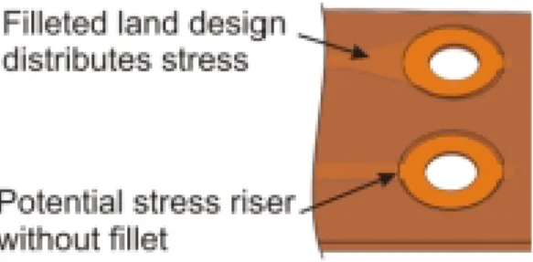
Figure 5-12 The practice of fi lleting pads helps to improve the reliability of the circuit by more evenly distributing stresses at the junction of the circuit land to the coverlayer opening.
FILLETINGOF LANDSAND PADS
Termination lands and pads on fl exible circuits should be fi lleted. Th is process increases pad area and helps to distribute stresses local to the coverlayer openings better, eff ectively relieving a stress riser condition that commonly causes failure if the fi llet is not supplied or ignored. Earlier CAD systems had diffi culty in producing these features, but today’s more advanced systems can more reliably address the requirement for fi llets without diffi culty. See Figure 5-12.
PADOR LAND HOLDDOWNSFOR SINGLE-SIDED FLEX
Termination pads on single conductor layer circuits and surface mount lands on fl ex circuits of any layer count may require special land hold down techniques. With single-sided fl ex circuits, the use of special features variously referred to as tie down tabs, anchoring spurs, or rabbit ears may be employed to prevent the land from lift ing during soldering processes in cases where excessive heat is used. With new lead-free solders, this may become more important.
An important note on this subject is that features such as tie down tabs could well cause problems as the industry moves to higher data rate signaling, and they should be used with caution. Th e stubs associated with some tie down features are capable of acting like antenna and can broadcast noise within the package when higher frequencies are used. Th us, an evaluation of the approach may be warranted, depending on the nature of the design. Figure 5-13 shows typical hold down tab features and alternative designs.
Figure 5-13 Various pad designs to help facilitate their capture by the coverlayer. (A) Standard fi lleted pad with full pad capture (B) Standard fi lleted pad with hold down tab (C) Overlapping pad design (D) Oval
pad design (E) Corner entry to square pad (F) Plated through holes normally require only fi lleting.
SURFACE MOUNTING LANDSFOR FLEX
Surface mount in combination with fl ex circuit technology is now very popular as the world’s fl ex circuit designers look to the success of Japanese products, which oft en employ fl ex circuits with surface mounted components. Surface mounting lands, however, oft en require a slight modifi cation of standard design rules when applied to fl ex circuit applications.
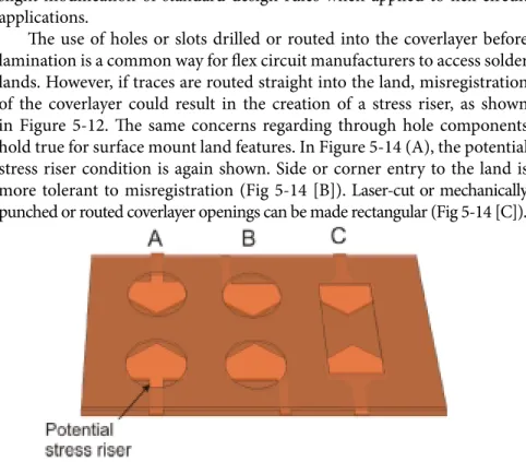
Th e use of holes or slots drilled or routed into the coverlayer before lamination is a common way for fl ex circuit manufacturers to access solder lands. However, if traces are routed straight into the land, misregistration of the coverlayer could result in the creation of a stress riser, as shown in Figure 5-12. Th e same concerns regarding through hole components hold true for surface mount land features. In Figure 5-14 (A), the potential stress riser condition is again shown. Side or corner entry to the land is more tolerant to misregistration (Fig 5-14 [B]). Laser-cut or mechanically punched or routed coverlayer openings can be made rectangular (Fig 5-14 [C]).
Rectangular openings can also be achieved by using photoimageable cover fi lms in place of a coverlayer. When accessing component lands for device assembly, it is recommended that solder lands extend beneath the coverlayer, as shown in Figure 5-15.
SMT device lands for both discrete and leaded devices should be extended to allow capture by the coverlayer. Normally, lands should be 250-375µm (0.010 to 0.015") larger to facilitate land capture and prevent undesired lift ing of the land during assembly or repair.
As with single-sided through hole lands for fl ex circuits, the objective is to prevent land lift during soldering operations and to provide extra strength against component pull-away in operation. Th is is of greater importance with components of greater mass. Figures 5-15 and 5-16 provide examples of common approaches used to access surface mount features in fl exible
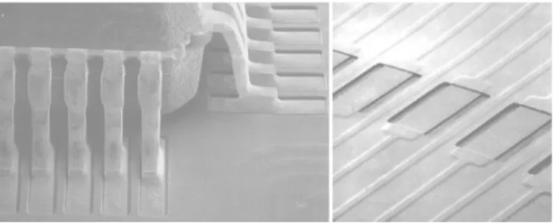
Figure 5-15 Examples of precisely photoimaged cover fi lms for surface mount lands on fl exible circuits (Photo courtesy DuPont)
Figure 5-16 The coverlayer openings for peripherally leaded SMT lands can be accessed either discretely or in gang fashion, by prerouting or punching the coverlayer before
circuit design applications while maintaining hold down capability. LANDSFOR PLATED THROUGH HOLES
Except for the shared need for fi lleting, double-sided fl ex with plated through holes does not require tie-downs, due to the rivet eff ect from the plated through hole. Th is inherent feature of the plated through hole serves eff ectively in preventing the pad from lift ing away from the surface of the fl exible circuit during soldering processes, should excessive temperatures be used in the assembly operation. Plated through holes are especially advisable if very small pads are required by the design to ensure formation of a reliable solder joint. Th is may require the addition of a second layer of copper, thus making a single-sided design a double-sided one. But, ease of processing and increases in reliability should, hopefully, off set any increases in cost.
BUTTON PLATING
An alternative plated through hole construction can be created using a process called button plating. Th e process can best be characterized as one where through holes and vias are selectively plated with copper. A fi nished structure can be seen in Figure 5-17.
Th e basic idea is relatively simple, however, success requires reasonable care in the manufacturing process. In practice, the manufacturer fi rst drills and makes conductive the hole walls of the fl ex circuit using a suitable technology (electroless copper or graphite coating). Th e manufacturer
next takes the panel in for imaging, where the panel is coated with a photoimageable plating resist, and the holes and vias to be plated are exposed and developed. A copper pattern plating step follows, and the hole walls and annuli of the holes are plated to the specifi ed thickness. Th at resist is stripped away, and a second plating resist is applied and exposed to create a positive circuit image, which can then be etched to create a metal circuit pattern. Th e holes and vias are tented over in this process. Th is action prevents the metal etching chemistry from entering the vias and etching out the holes, thus creating electrical opens.
C
OVERLAYERANDC
OVERCOATC
ONCERNSAs mentioned earlier in the section on fl ex circuit materials, there are several types of fl exible covercoating systems available. Each has its own special applications and advantages. Included among them are the following:
Adhesive-backed fi lms
Adhesive-backed polymer fi lms are the type of coverlayer most frequently specifi ed and used by fl ex circuit designers and manufacturers. It is also the fl ex circuit covering method best suited to dynamic fl ex circuit applications because of the balanced material properties from side to side.
Screen-printable liquid covercoats
Applied and cured by simple means, screen-printable liquid covercoats are the least expensive covercoat type and the one most oft en used with polymer thick fi lm and simple single-sided copper constructions.
Photoimageable liquid and fi lm polymers
Newer methods for covercoating fl ex circuits involve the use of photoimageable polymers. Th e results have been very promising. In process, the fl ex circuit is coated with a polymer fi lm, which can then be imaged and developed to access termination features. Th is method, which looks quite good for many applications, could help put an end to many of the coverlayer misregistration problems manufacturers have had with small features and, in addition, quell concerns over adhesive squeeze-out onto lands.
In most fl ex circuit designs, the coverlayer or covercoat serves more than one purpose. For example, covercoats commonly function as a solder mask, helping to prevent solder from shorting circuit traces together, and serve to isolate electrically and protect physically the circuit from damage. In addition, as described earlier, coverlayers serve to help restrain the pads physically and hold them in place during soldering, preventing pad lift . Th e coverlayer (or possibly a covercoat) also allows conductors to be placed in the neutral axis for improved fl ex and bending performance. Th is subject will be covered in more detail later in the chapter.
Given the diversity of the roles fl ex circuits play in electronics packaging, it is understandable that it has been diffi cult for suppliers to come up with a universal solution that is at once low cost, high performing and easy to apply. Nevertheless, steady progress is being made by material suppliers, and new solutions are regularly being developed and off ered to the industry.
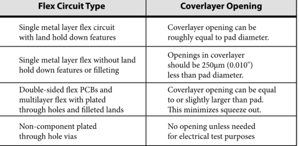
SIZING COVERLAYER OPENINGS
As was seen in the discussions on surface mount land design, the sizing of coverlayer openings varies according to pad design features and with the
number of metal layers. Again, the key area of concern is with single-metal-layer fl ex circuits, where potential pad lift demands special care in design. Table 5-3 provides general guidelines for sizing of coverlayer openings. TRACE-TO-CUT LINE CONCERNS
Best current practice for fl ex circuit design generally recommends that the edge of the part to the edge of conductor spacing be >1.25mm (0.050"). It has been shown, however, that circuits can be made reliably with edge- to-conductor spacing of ≤ 250µm (0.010"), although this normally comes at increased cost, which will vary depending on the tooling system used. Refer to Table 5-1 on page 77.
Flex Circuit Type Coverlayer Opening Single metal layer fl ex circuit
with land hold down features
Coverlayer opening can be roughly equal to pad diameter. Single metal layer fl ex without land
hold down features or fi lleting
Openings in coverlayer should be 250µm (0.010") less than pad diameter. Double-sided fl ex PCBs and
multilayer fl ex with plated through holes and fi lleted lands
Coverlayer opening can be equal to or slightly larger than pad. Th is minimizes squeeze out. Non-component plated
through hole vias
No opening unless needed for electrical test purposes
Table 5-3 Coverlayer opening guidelines vary with the nature of the design.
T
EAR-R
ESISTANCEF
EATURESINF
LEXD
ESIGNAll fl ex circuit designs should be made as tear-resistant as possible. While the material may not be intrinsically tear-resistant, tear-resistance can be improved by employing certain features in the design. Th ere are several possible methods, described below and illustrated in Figure 5-18.
All of the following techniques have been successfully used to help prevent tearing. One or more of the following techniques can be used:
Radius All Internal Corners
Th e fi rst line of defense against tearing is to make certain that all internal corners are provided with as generous a radius as possible. Th is design practice is the most important and simplest of all methods used to prevent tearing of the fl ex circuit material.
Leave Metal in Corners
Th e circuit design should, if possible, have small areas of copper provided for at internal corners to serve as tear stops at the inside of corner radii. Th is serves to prevent further or imminent propagation
of a tear through the polymer, should a tear in the material start.
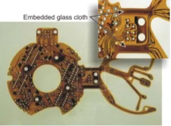
Laminate Glass Fabric in Corners
Glass cloths can be laminated into corners during the fabrication process. Th ough not fl exible, this method has been shown to provide a very robust corner construction and has been favored in the past by military product designers. It is an expensive solution, however, because of the type of preparation required and should be used only aft er careful consideration of the alternatives. (See Figure 5-19.)
Use Fluoropolymer Coverlayer
Th e use of fl uoroplastics such as Tefl on® as coverlayers helps to improve
tear resistance by virtue of the high tear resistance of the polymer itself. Th is is due to the fact that fl uoropolymer tends to stretch rather than tear, adding toughness to the substrate. An additional benefi t of using fl uoropolymer coverlayers for those involved in high frequency design is that the dielectric constant of the coverlayer is much lower.
Use of Radiused Slots
Th e use of slots with ends that have a radius to access relieved circuit features also can serve to provide tear resistance. Normally, such features can easily be provided for during the punching operation or other circuit fabrication process.
Drilled Holes at Corners or Ends of Slits
Drilled or punched holes in corners or at the ends of access slits have been used with success when fl exible appendages must be spaced close together. Th is method allows the greatest use of material, but the hole size chosen will impact tear resistance. If the hole is very small, the overall robustness will be reduced.
Aramid Fibers Inside Cut Line
As an alternative to glass cloth, the use of aramid fi bers routed through corners or along the entire outline of the fl ex circuit is a unique method to stop tearing of fl ex circuits. Th e thin polymer fi bers have very high strength and are very pliable, minimally aff ecting fl exibility. However, this is a labor intensive method and should only be specifi ed with the knowledge of cost impact.
Ultimately, the choice of which method to use to restrain or prevent tearing of the fl ex circuit is not of overriding importance. What is very important is that the designer makes certain that some suitable method to protect against tearing is used.
is here reemphasized that square or sharp internal corners are an invitation to trouble and should be studiously avoided. If the area of the corner is to be permanently bonded to a rigid base, then it is less important but still recommended that a radius be used.
S
TIFFENERSANDR
EINFORCEMENTSFORF
LEXStiff eners or reinforcements are commonly used to support components
on fl ex circuits. Th ese important “add-ons” can be fabricated from a wide range of materials, depending on design need. Th e choice of material is predicated on what objectives are sought (low weight, best heat sinking, lowest cost, best spring qualities, etc.). Th e materials referenced in Table 5-4 have all been successfully employed to reinforce fl exible circuits.
In addition to materials mentioned in the table, the package or box
Figure 5-18 Tear-resistance features are important. A number of methods for tear restraint work well for fl ex. Shown above are: (1)Large radius in corner (2)Embedded glass cloth (3)Recessed slot
(4)Hole in slit (5)Drilled hole at corner (6)Embedded aramid fi ber (7)Extra copper in corner
into which the circuit is to be placed can also be used as the stiff ener if the design allows. Beyond simple component support, this technique allows the package or box itself to be used for heat dissipation. While a potentially attractive solution for a number of applications, the diffi culty of this method comes to light if repair is required, because removal can damage the circuit.
RESIN-GLASSLAMINATES EXTRALAYEROFCOVERLAYER
THERMOPLASTICSHEET BERYLLIUMCOPPER
STAINLESSSTEEL ANODIZEDALUMINUM
INJECTIONMOLDEDBASES QUARTZGLASS
Table 5-4 Stiff ener Material Choice for Flex Circuits. A wide range of materials, both conductive and insulating, can be used to provide stiff ness to a fl ex circuit where required. The table above
notes some of the materials that have been used for diff erent applications and needs.
SPECIAL TECHNIQUESFOR STIFFENERS
Special design techniques allow stiff eners to serve more than the function of component support. For example, while the primary purpose is to support components, stiff eners can be so designed as to aid assembly by enabling the fl ex to be assembled as virtually a rigid board. Th is can be accomplished by using one of the following techniques.
Figure 5-20 Gang assembly or mass application of stiff eners in panelized form facilitates both the application of the fl ex circuit to the stiff ener and subsequent component assembly. When the fl ex circuit and stiff ener
are bonded together, the resulting fl ex circuit panel can be processed much like a rigid board. Note that the adhesive is applied oversized and cut to dimension before the routing step is performed.
ROUT-AND-RETAIN STIFFENERS
Rout-and-retain stiff eners are produced by CNC routing of the substrate so as to leave it attached in certain locations for easy removal later. Such constructions allow the stiff ener to be snapped or cut off aft er assembly. (See Figure 5-20.)
While routers are pervasively used in circuit manufacturing, lasers and water-jet cutters are other potential manufacturing choices for preparing or pre-cutting stiff eners
RETURNTO WEB PUNCHING
Return to web punching (also referred to as “punch out, punch in”) of the stiff ener requires special punch tooling wherein the rigid material is punched out of the panel and then immediately pushed or punched back into its original position in the panel. Th e method is commonly used for inexpensive rigid boards and allows mass assembly with relatively simple assembly fi xture requirements.
SCORINGOR DICINGOF STIFFENERS
If features of the fl ex circuit design allow the use of scoring or dicing tools to prepare the stiff ener panel is potentially possible. With respect to the scoring process, the circuit and/or the stiff ener is cut partially through, using special tools which cut a controlled-depth straight path through the rigid circuit material. Th e cut can be made through the rigid material alone or through both fl ex circuit and rigid base. Aft er component mounting and assembly, the circuits can be snapped apart along the score lines.
In contrast to the routing concept shown, the other alternative— dicing—requires cutting completely through the circuit and stiff ener. Because of the nature of the tools used, all material cuts must be made in a straight line and orthogonal to the major (X&Y) dimensions of the panel. ADHESIVESFOR BONDINGOF STIFFENERS
All of the bonding adhesives used in the creation of fl ex circuit laminates are candidates for attaching a fl ex circuit to a stiff ener. Th e choice of which adhesive to use is most oft en a function of performance requirements.
It is worth checking with the fl ex circuit vendor for his recommendations. Beyond those adhesives used in normal fl ex circuit construction, there are other types of adhesives that can be used as well. Following are some of the more commonly used adhesives for stiff ener attachment.
PRESSURE-SENSITIVE ADHESIVES
Pressure-sensitive adhesives are very commonly used to attach stiff eners. Th ey are perhaps the most versatile and easiest to use. Th ey exhibit very good bond strength, which in some cases actually improves
with age. Th ese adhesives are not generally designed for extended use at high temperatures but are for the most part limited to enduring only short excursions at high temperatures (soldering temperatures). Again, with lead-free solder technology moving ahead, there is need to check capabilities when using higher-temperature lead-free solders.
One particular advantage PSAs off er over other adhesive choices is that, when applied directly to the fl ex circuit, they allow for the fl ex circuit to be bonded to virtually any surface, thus eff ectively making anything in the package a potential stiff ener.
THERMOSETTING ADHESIVE FILMS
Th ermosetting adhesive bonding fi lms (cast-acrylic fi lms or fl ex circuit bondplies) can also be used to bond fl ex circuits to stiff eners, but they require the time and expense of an additional lamination step. Even so, thermosetting fi lm adhesives can off er very high bond strength of the fl ex to the stiff ener.
LIQUID ADHESIVES
One and two part liquid epoxy type adhesives have been used for bonding stiff eners to fl ex circuits. Th ey are diffi cult to apply uniformly and thus do not enjoy wide popularity. Such adhesive materials are well suited for—and can be well applied in—the creation of strain relief at the transition edge of the fl ex and stiff ener by creating a bead of epoxy along the entire edge of the transition.
THERMOPLASTIC ADHESIVE FILMS
Th e use of thermoplastic-based adhesive fi lms for bonding fl ex circuits to stiff eners is another common option. Th ermoplastic fi lms have some unique advantages among adhesives in that they are low-stress, fully-polymerized polymer resins that require no cure. With properties that include adhesion to a wide variety of surfaces and materials, and the reported ability to be reworked easily, these adhesive materials may see expanded service in the future.
UV CURABLE ADHESIVES
Ultraviolet curable adhesives are another potential adhesive choice for stiff ener attachment. With some screen-printable formulations, the UV “activates” the polymer, creating a tacky adhesive with PSA qualities. In addition, because they can be rapidly cured, these adhesives are also an attractive choice for relieving strain on the fl ex circuit at the transition point from rigid to fl ex.
HOLESFOR STIFFENERS
of the circuit or breaking of the copper at the transition point can more easily occur if the procedure is omitted from the design or manufacturing process. One or both of
the following techniques should be used.
ROUNDED STIFFENER EDGESAT
TRANSITION
Th e stiff ener edges in areas where the fl ex circuit egresses from the perimeter of the stiff ener should be rounded or provided with a radius at the edge to prevent a
point of focused stress. Alternatively, breaking the rigid stiff ener with a fi le or sandpaper at the transition edge before assembly can provide a similar benefi t.
FILLET TRANSITION EDGEOF STIFFENER
Filleting of the transition edge of a stiff ener with a resilient adhesive or epoxy is another common method of strain relieving circuits. Th e small bead of a suitable polymer will provide a simple means of transitioning strain from the stiff ener to the fl ex circuit. Figure 5-23 illustrates the two approaches.
STRAIN RELIEFFOR UNSUPPORTED FLEX CIRCUITS
Strain relief should also be provided when mounting the fi nished circuit or assembly. Th e following methods can be used for this purpose:
1) Break or radius sharp edges of any retaining bars or clamps may be used to hold the fl exible circuit in place.
2) Use a low modulus, elastomeric material between restraining bars and the fl ex circuit.
3) Bond the circuit to the assembly housing, using a double backed adhesive foam material or simple pressure-sensitive adhesive.
Figure 5-22 Mounting holes should retain copper when fl ex circuit is to be mounted without mechanical support.
and those for fi nal fl ex circuit assembly mounting, have diff erent purposes and oft en somewhat oppositional requirements. Th e result is that the design rules can vary considerably, depending on the application. Explanations as to how to determine the appropriate size follow. Figure 5-21 illustrates the concept.
COMPONENT HOLESIN STIFFENER
Holes in the stiff ener for through hole mounting of electronic components, such as dual in-line packages (DIPS), should be 250µm-375µm (0.010-0.015") larger than the through holes in the fl ex circuit (which, in turn, are by design rule 250µm [0.010"] larger than the lead). Th is is to allow for any movement and misregistration between fl ex and stiff ener that might occur during the stiff ener lamination or bonding process. Th is technique also helps to assure the greatest opportunity of accessing the through hole with the component lead without interference from the stiff ener.
ASSEMBLY MOUNTING HOLES
Holes in the stiff ener for mounting the assembly should be equal to or slightly smaller in diameter than the holes in the fl ex. Th is assures that the stresses are placed on the rigid portion of the assembly and not on the fl ex circuit. Th is is not an ironclad rule, as it is possible to mount the fl ex circuit directly to a carrier without a stiff ener, using common mounting hardware if necessary.
UNSUPPORTED MOUNTING HOLES
Mounting holes that are not supported by a stiff ener should be designed to maintain copper around the hole for added strength. (See Figure 5-22.) Th is practice is of value with regular mounting holes, as well, if the design will permit. Such features are also a convenient means of making a connection to ground.
S
TRAINR
ELIEFFORF
LEXC
IRCUITSTh e provision of strain relief at the edges of stiff eners helps to prevent stress risers from occurring at transition areas from fl ex to rigid. Tearing
Figure 5-21 Access holes through the stiff ener fi ll diff erent needs. Holes in the stiff ener for leaded components are made slightly larger than holes in the fl ex circuit. This allows for any movement during the stiff ener lamination
M
ETHODSOFC
ONNECTINGF
LEXC
IRCUITSConnecting a fl exible circuit to other elements of an electronic system is a vitally important element in system design, manufacture and assembly. Th ere are numerous methods of making connection to fl exible circuits. Virtually all connector manufacturers have connectors either specially built for, or readily adaptable to, fl ex circuit designs.
One innovative connector manufacturer of record, Beta Phase, Inc. (Menlo Park, Calif.), actually made its connectors out of fl exible circuits, producing high-performance connectors with very high pin count equivalents. Th e concept was much ahead of its time and did not get much use outside of extreme performance applications, such as the Cray supercomputer, but the technology was purchased by Molex, and some elements of the earlier concepts are now available. As well, other connector manufacturers now have comparable product in the market.
FLEXIBLE CIRCUIT CONNECTOR TYPES
Some basic connectors are relatively simple devices. Examples include insulation displacement and crimp-type connectors. Th ese have proven popular in applications where cost is important. Th ey are not generally considered suitable for high-reliability applications, however.
To make both male and female pin in socket type connectors, swaged or brazed pins can be attached directly to the fl ex circuits. Th ese have also brought some success in certain low-end product areas where performance is not a key concern.
Figure 5-24 Patent drawings of a novel high density fl exible circuit based connector invented by John Krumme and Gary Yasumura while they were at Beta Phase. A shape
Th e Sculptured® fl ex circuit technology described earlier has the ability
to integrate the connector directly into the fl ex circuit itself. Th e method is suitable for a number of diff erent electronic applications, due to the fact that no discrete joining of pins to the fl exible circuit is required. By using this technology approach, it is possible to have edge contacts that extend, unsupported, beyond the edge of the fl ex circuit. It is then possible to simply post-form the leads as required to create a viable male pin connector for mating with a compatible socket.
In addition, or as an alternative to the sculpturing method described, edge card contact constructions can be created by folding the contact area of a fl exible circuit around a stiff ener. Th is is a simple and relatively inexpensive way to interconnect a fl ex circuit. It is directly analogous to edge card contacts on rigid boards, for which there are numerous types of mating connector solutions
available. Because the fl ex circuit itself is thin, it is possible to accommodate a wide range of connector designs simply by altering the thickness of the stiff ener (see Figure 5-26).
Surface mounted connectors are an increasingly important and common connector choice for use with fl exible circuits, for obvious reasons. With size reduction a common objective
Figure 5-25 Historical approaches for soldering military style two part connectors to fl ex circuits. A key concern is inspection, as solder joints are hidden by each successive layer.
Figure 5-26 Surface mount connectors for fl exible circuits facilitate high density interconnection.
of fl exible circuit technologies, it comes without surprise that low-profi le connectors are well-suited to the needs and abilities of fl ex circuits.
A number of low-profi le connectors are presently in the market. Th ese miniature connectors are very nicely suited to many space-constrained fl exible circuit applications. Low-profi le connectors known as low- insertion-force (LIF) and zero-insertion-force (ZIF) connectors that can handle contact pitches down to 0.30mm (.012") have been produced by commercial manufacturers. Th e profi le height for such connectors can be as low as 0.60mm (.24").
Another option for low profi le interconnection of fl exible circuits is lapped connections. Solder, conductive polymers and adhesives have all
Figure 5-26a Ends of the fl exible circuit can be converted to an edge card contact by placing a stiff ener behind the fl ex and folding and bonding the fl ex to the stiff ener.
Figure 5-27 Low profi le connections of fl ex circuits can be accomplished in many ways. Both permanent and separable connections are possible. Shown above are but a few examples.
been used to make lapped connections between a fl ex circuit and a mating interconnection structure. It is a reasonably common method; for example, a large percentage of fl at panel displays are connected using anisotropic adhesives.
Another unusual design approach to making fl ex circuit interconnections is one wherein the connections are made directly between chips, using anisotropic adhesives or lap soldered connections. Th is approach has been proven, both by modeling and manufactured prototypes, to be capable of providing very high speed and low power.
To summarize the topic, connecting the fl exible circuit to a next level or associated interconnection device or system can be accomplished using one of many options. Th e choice is predicated on the cost and performance requirements of the end product. Th e examples provided are not exhaustive in terms of options, but they are representative.
B
ENDINGANDF
LEXINGD
ESIGNC
ONCERNSWhile fl ex circuits typically are employed simply to allow the user to form the circuit to fi t the shape of the package (fl ex to install applications), there are still many applications that require some dynamic fl exing. In fact, in most applications, the very act of placing the fl ex circuit into the assembly requires that the circuit be bent or folded. In some applications this can occur several times. Flexible circuits are capable of enduring many millions or even billions of fl exural cycles, provided the design is properly matched to the task.
Th ose not involved in dynamic fl ex design should also take to heart the
Figure 5–28 Making fl ex circuit connections directly between chip packages can provide signifi cant performance improvements. (Courtesy SiliconPipe, San Jose, CA)
lessons of this process. For example, it is important to remember that even static fl ex circuits can be dynamically cycled by virtue of their application and design. Such events are common occurrences in circuits designed for any type of mobile equipment, such as automobiles and planes.
For example, shock and vibration encountered by a vehicle can cause a fl ex circuit to endure millions of low amplitude, high frequency fl ex cycles. If dynamic fl ex design rules are not taken into account or are simply ignored, the potential for unexpected cyclic fatigue failure of an application subjected to shock and vibration exists. Attention to the few simple rules for dynamic fl ex provided here can benefi t many fl ex circuit applications. Th ey are, arguably, good practice for all fl ex circuit designs.
BENDINGAND FLEXING TECHNIQUES
A number of clever approaches and techniques have been developed by engineers over the years to achieve the desired bending or fl exing motion in a fl exible circuit. Th e types of motions employed range from linear ex-tension and contraction to rotational fl exing through various small angles of 5° or 10° to more than 360°. Figure 5-29 provides conceptual examples.
AVOID PLACEMENTOF THROUGH HOLESIN BEND AREAS
An important design practice that is sometimes overlooked or ignored is the avoidance of placing plated through holes in the bend areas. Th is is of particularly great importance in dynamic applications. For static applications, it may be possible to place vias through a bend successfully if they have a coverlayer and if the bend radius is large enough. Th at said, it is still a practice that should be avoided.
Figure 5-29 Various fl exing and bending methods are illustrated. Clockwise from the bottom left: accordion fl ex, rolling fl ex, counter rolling fl ex (must be vertically space constrained), “window shade” fl ex, large radius or hinge type fl ex and coiled fl ex.
ROUTE TRACESAT 90° THROUGH BENDAND FOLD AREAS
Conductor traces should be routed through bending and fl exing areas at 90° (perpendicular) to the bend line. Th is is an intuitively natural rout-ing scheme and serves the purpose of bendrout-ing well. However, the rule is somewhat fungible and seems to be violated regularly for matters of con-venience. For example, in some hinge circuits (see Figure 5-33), the traces may be bent in more than one direction to achieve the design purpose. ROUTE CONDUCTORS ON A SINGLE LAYER THROUGH BEND W h e n e v e r possible, conductors should be routed on a single metal layer through bend and fold areas to enhance fl exibility. When not
possible, the conductor should be staggered from side to side to avoid the I-beam eff ect discussed earlier.
DESIGNTO KEEP COPPERIN NEUTRAL AXIS
Th e concept of neutral axis is very important to fl exible circuits. In theory, the center of any item being bent is nearly immobile, with stress being absorbed by the outer layers of material. Th erefore, if the copper (or other metal) foil is kept to the center of the design, the fl exing life should be enhanced. (See Figure 5-31.)
Many experiments have verifi ed this theory. Data provided in the graph in Figure 5-32 dramatically illustrate the eff ect that neutral axis placement can have on the fl exing life of a fl ex circuit.
FLEX DYNAMIC AREASWITHTHE COPPER GRAIN DIRECTION
Th e orientation of the grain of the copper foil has a defi nite eff ect on fl exural life of a design. Grain direction is of greatest importance with fl ex circuit designs fabricated using rolled and annealed (RA) or traditional
Figure 5-30 It is preferred practice to route traces through bend areas in a single metal layer. If two metal layers are
required, the traces should be off set or staggered.
electro-deposited (ED) copper foil. With vendor-electroplated copper on sputtered fi lm, orientation is not as critical, as there is no specifi c grain direction. Th e eff ects of grain direction on fl exural life can be very signifi cant, as the data found in the graph in Figure 5-32 indicate.
NOTES:
1) The unbalanced construction consisted of 25µm polyimide with 25µm adhesive on a base of 50µm polyimide with 25µm adhesive and one-ounce copper.
2) The semi-balanced construction used adhesive to achieve the desired balance (25µm polyimide with 50µm adhesive). The base was the same as above.
3) The balanced construction had a coverlay makeup that matched the base material exactly (50µm polyimide with 25µm adhesive).
KEEP FLEXURAL ARC SMALL
For maximum fl ex life, it is best to keep the range of the fl exural arc or total angle of fl exure of the circuit for
dynamic designs as small as possible (that is, fl ex the circuit over the smallest possible distance). Th is is a key technique used in later-model disk drive applications to allow them to achieve their present high-fl ex-life cycling.
PROVIDETHE LARGEST BEND RADIUS POSSIBLE
Th e designer is advised always to provide the largest practical radius through bend areas. Th is design approach is especially important for dynamic fl ex, but,
as has been previously noted, it can also be fl ex design concept for a cellphone Figure 5-33 Example of a hinge (Source: US Patent No. 6948240) Figure 5-32 Data show construction infl uence on fl exural endurance.
important in fl ex applications that are apparently static in nature.
Th e graphic and simple equation in Figure 5-34 illustrate the eff ect of bend-radius diameter on the copper foil. As can be concluded by calcula-tion, the elongation requirements for the copper foil rise signifi cantly as
bend radii decrease.
GUIDELINESFOR MINIMUM BEND RADII
While fi nite element modeling can provide excellent predictive data for suggesting bend limits, there are some common guidelines that have long served to keep the design inside the limits. For normal bending of fl exible circuits, those guidelines can be found in Table 5-5. For very high fl ex life dynamic fl ex circuit designs, fabrication and testing of prototypes commonly remains the preferred method of design verifi cation.
Flex Circuit Type Minimum Bend Radius Single Metal Layer 3-6 x circuit thickness Double-sided Flex 6-10x circuit thickness
Multilayer Flex 10-15x circuit thickness (or more) Dynamic Application
(Only single-sided recommended)
20-40x circuit thickness
(increase in bend radius increases life)
Table 5-5 Minimum bend radii design guidelines for fl ex circuits
CREASINGAND FOLDING FLEX CIRCUITS
Creasing and hard folding of fl ex, while not a preferred practice, can be successfully accomplished with some attention to certain details. When required, circuit should be bonded to prevent it from bending back at the crease or fold line. Strain relief is also recommended. As noted earlier, it is important to keep the construction balanced for best fl exural endurance life. Th e ideal copper for such strain-bending applications will be a low strength, high-elongation copper. Fully annealed soft copper is normally a good choice for applications requiring a small radius bend.
B
ENDINGF
LEXC
IRCUITSTOH
OLDS
HAPEWhen bending fl ex circuit products for static, form-to-fi t applications, holding shape is a desirable condition. However, fl ex circuits sometimes have some elastic memory. Th e following principles for shaping fl exible
Figure 5-34 Small-diameter bend radii demand greater elongation from materials used in fl ex
circuits to fi t permanently in their application will help to overcome the condition. Th e fi rst principle is maximizing the metal area. Copper, or any other metal one might use for the conductors, will permanently deform plastically when bent beyond its elastic limit.
Many polymers (elastomers are generally excluded, although they can take a set over time) will also permanently deform if their elastic limit is exceeded; their limit, however, is many times greater than that of metal. Th us, when the composite structure that we now call a fl ex circuit is bent, the metal has plastically deformed, while the polymer is still likely to be in its elastic range.
PROVIDEFOR METAL DOMINANCEIN BEND AREA
In order for the copper (or other metal) to prevent the polymer from snapping back, it must overwhelm the elastic memory of the polymer. Copper is stronger and higher in elastic modulus, but if the traces are small or the copper is a low percentage of the local area, the remnant elastic strain in the polymer may cause the fl ex circuit to regress to its original fl at shape. Th is method is in keeping with the practices used by fl exible circuit manufacturers to help maintain dimensional stability.
WIDENED CIRCUIT TRACES THROUGH BENDING ZONE
If circuit weight is a concern, the area of extra copper can be localized. In such cases, the circuit features are widened in the area of the bend and then reduced in width again as they enter and exit (see Figure 5-36). Circuit traces should taper to the new width in both directions.
DETERMINING BEND AREA LENGTH
As to the potential question, Th rough what length of the bend area should the traces be widened? A simple method to get a fi rst order approximation is to determine the circumference of an imaginary circle having the desired bend radius, and multiply that result by the bend angle divided by 360 (the degrees in a circle). Th is should ensure that a suffi cient
Figure 5-35 Very small bends in the fl ex circuit are possible, as demonstrated in this fi gure (from a disc drive application).
amount of the bend area is fi lled with the wider copper traces. However, a little extra length may be required, depending on the construction.
USE THICKER COPPERIN BEND AREA
If widening the traces alone does not help suffi ciently, then one of two analogous methods can be used. One can either use a thicker metal foil or use a thinner fl exible base material. Th e objective remains the same: Make certain that the metal can overwhelm the polymer in order to hold the fi nal shape. Th ere are advantages and disadvantages to both paths. Making the copper thicker may make etching a bit more diffi cult; it will also take longer to etch and will use more chemistry. On the other hand, making the polymer thinner could make handling a bit more diffi cult, and the strength of the fi nal assembly will not be as great as with the alternative method.
P
ERMANENTS
HAPINGA
LTERNATIVESSlight over-driving of the bend to create a stable, more permanent shape can be used to advantage, with the caveat that the minimum bend radius for the fl ex construction not be violated. Note that when permanently bent and plastically deformed, the copper is normally thinned in the area of the bend, and is thus weakened. If a truly accurate predictive solution is desired, one can use fi nite element modeling methods.
HEAT FORMING
Another way to get the fl ex circuit to hold shape is to form it (usually using a mandrel of some sort), bend the circuit into shape, and then apply heat to the fi xture, allowing it to cool in place. Th e objective is to relieve all of the remnant elastic strain in the polymer by allowing it to deform plastically to the fi nal shape with the addition of heat. Th is approach works easiest with polymers and/or adhesives
t
hat have relatively low melting points. It is a very common method for making dome switches in polymer thick fi lm circuits using polyester base materials.Figure 5–36 To create a permanent bend, copper traces can be made wider through the bend area.
In contrast, polyimide has a very high melting temperature, making it a less attractive candidate. In this method, one must normally rely on the ability to get above the glass transition temperature of the adhesive and allow the circuit to cool back below that temperature before releasing it from the mandrel.
USEOF LOW-MODULUS POLYMERS
A fi nal choice for permanent shaping is to use nontraditional base materials. Th ese would be materials of low strength and having little if any elastic strength. Unreinforced FEP or PTFE [Tefl on], for example, falls into this category. Th is combination will allow the user to deform the circuit permanently into the desired shape. Th ere are other options that are variations on one or more of these themes, but these are the basics.
Summarizing this topic, keeping and holding fl ex circuits in shape is not that diffi cult, but it does take some attention. Th e method of choice relative to those mentioned above will, obviously, depend on the demands of the design and its application.
F
INITEE
LEMENTM
ODELINGOFF
LEXOver the years, with increases in computing power and increased availability of memory, there has been a signifi cant improvement in fi nite element modeling tools, in terms of both cost and performance. Th us, it is not surprising that—given the importance of the mechanical requirements to the long-term performance of a fl exible circuit assembly—many com-panies are beginning to perform fi nite-element modeling of the circuits to validate the design
be-fore committing the product to manufacture. Th is can be much more cost eff ective than iter-ating through a num-ber of prototype runs, provided the modeling parameters are properly selected.
FEA tools are wide-ly available and many can accept data directly from many types of de-sign soft ware and the user need only input
Figure 5-37 Finite element modeling can signifi cantly improve the chances of fi rst-pass success in design for application by providing valuable information about the location and magnitude