PD39210
PoE PSE Controller
Introduction
The PD39210 is a member of the Microchip Generation 6 family of PSE controllers. The device when used with the Microchip PD39208 PSE manager is an optimized IEEE® 802.3af/at Power Sourcing Equipment (PSE) solution. The Microchip Generation 6 family of PSE controllers includes the PD69210, PD69220, and PD39210 devices. The PD69210 and PD69220 have an identical feature set and differ only in physical pinout. The PD39210 has an identical pinout to the PD69210, with a reduced feature set. The PD69210, PD69220, and PD39210 are based on the
Microchip SAM D21 family. The PD69210 and PD39210 are recommended for all new designs. The PD69220 is available for existing designs.
The PD39210 will support up to 48 2-pair logical ports and is available in a 32-pin, 5 mm × 5 mm QFN package.
Typical PoE Application
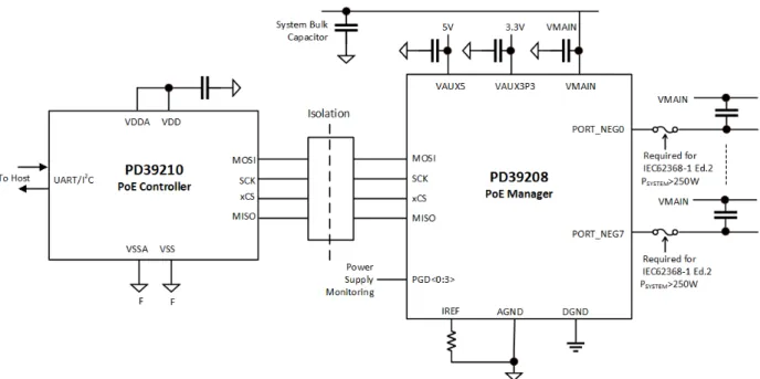
The following figure shows the typical PoE application using the PD39210 Controller and PD39208 Manager.
Figure 1. Typical IEEE 802.3af/at PoE Application
Features Matrix
Feature Description PD69210 PD69220 PD39210
Support IEEE 802.3af/at Y Y Y
Support IEEE 802.3bt Y Y N
Support HDBaseT (POH) Y Y N
Port control matrix Port matrix control enables to ascribe each physical port in the system to a logical port.
2p/4p 2p/4p 2p
Logical ports A logical port can be built from 2×physical ports or 1×physical port with PD69210 or PD69220. A logical port can be built from 1×physical port with PD39210.
48 48 48
Max 2-pair power 45 W 45 W 30 W
Power management The system supports three power management modes: Class (LLDP), Dynamic, and Static.
Per port Per port Per system No LLDP Power good Used to select the system power bank to be
applied to the specific PoE manager.
Y Y Y
Port power limit Configurable port power limit; when a port exceeds the limit, it is automatically disconnected.
Y Y Y
Interrupt pin Interrupt out from PoE controller. Y Y Y
Disable port pin Shuts down all of the PoE ports in the system.
Y Y Y
System OK indication System validity indication. Provides a digital output signal to the host or to control an LED to indicate system status. When the system is OK pin state is low.
Y Y Y
Legacy (reduced capacitance) detection
Enables detection and powering of pre-standard devices (PDs).
Per port Per port Per port LED stream A direct SPI interface to an external LED
stream.
Y Y Y
Fast PoE Ability of a system to quickly boot and power up ports without waiting for the host setting.
Y Y Y
Perpetual PoE Ability of a PoE system to maintain PoE power while upgrading host firmware or host is in reset.
Y Y Y
Communication Communication interface with host. I2C or UART I2C or UART I2C or UART
Communications protocol Compatible with previous generations controllers.
Table of Contents
Introduction...1
Typical PoE Application...1
Features Matrix... 2 1. Architecture... 4 1.1. Firmware... 4 1.2. Communication... 4 1.3. GUI... 4 1.4. Software Library... 5 1.5. SPI Communication...5 1.6. UART ...5 1.7. I2C ... 5
1.8. UART or I2C Address Selection... 6
2. Electrical Specifications... 7
2.1. Electrical Characteristics... 7
2.2. Immunity...7
2.3. Absolute Maximum Ratings...7
3. Pins... 8
3.1. Pin Diagrams...8
3.2. Pin Descriptions... 9
4. Package Information...11
4.1. PD39210 Package Outline Drawing... 11
4.2. Thermal Specifications... 12
4.3. Recommended PCB Layout...13
4.4. Recommended Solder Reflow Information...15
4.5. Reference Documents...16
5. Ordering Information... 17
6. Revision History... 18
The Microchip Website...19
Product Change Notification Service...19
Customer Support... 19
Microchip Devices Code Protection Feature... 19
Legal Notice... 20
Trademarks... 20
Quality Management System... 21
1.
Architecture
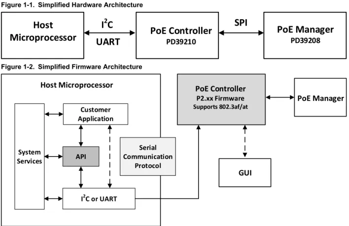
The following figures show the simplified hardware architecture and firmware architecture of the PoE system based on the PD39210 controller and PD39208 manager.
Figure 1-1. Simplified Hardware Architecture
PoE Manager
PD39208
PoE Controller
PD39210
Host
Microprocessor
SPI
I
2C
UART
Figure 1-2. Simplified Firmware Architecture
PoE Manager
PoE Controller
P2.xx Firmware
Supports 802.3af/atHost Microprocessor
GUI
Customer
Application
API
System
Services
Serial
Communication
Protocol
I
2C or UART
• Dark grey boxes indicate Microchip-supplied firmware. • Light grey boxes indicate Microchip-provided documentation. • White boxes are user-supplied.
1.1
Firmware
• Firmware is pre-programmed in PD39210. Firmware version is identifiable via the IC Ordering Part Number. • Firmware is vendor-agnostic with regards to choice of the host controller.
• May be operated standalone or with I2C or UART communication to host.
• Default profiles are coded into the firmware. Microchip offers a Configuration Tool for profile modification. • Firmware is field upgradeable via the I2C or UART link.
1.2
Communication
Communication between the host application and the controller’s firmware may be done via a 15-byte protocol.
Architecture
1.4
Software Library
Firmware (without the boot section), GUI, and API are available on Microchip’s Software Library.
1.5
SPI Communication
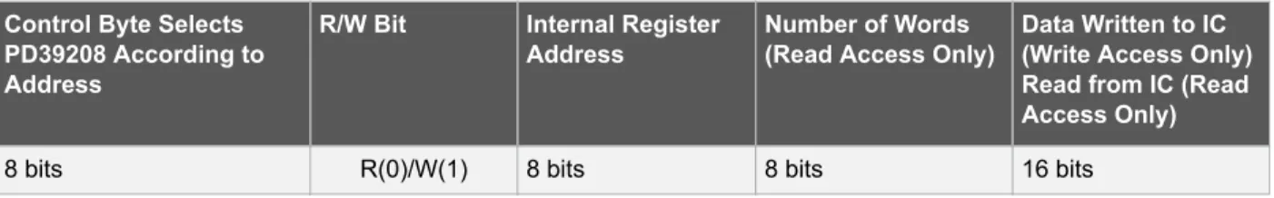
The PD39208 manager uses SPI communication in SPI client mode to communicate with the various controllers. Each manager has an address determined by ADDR0–ADDR3 pins. Each controller can support up to 12 ICs at addresses 0–11. The actual frequency between PD39210 and PD39208 ICs is 1 MHz.
The following table lists the SPI communication packet structure.
Table 1-1. SPI Communication—Packet Structure
Control Byte Selects PD39208 According to Address
R/W Bit Internal Register Address
Number of Words (Read Access Only)
Data Written to IC (Write Access Only) Read from IC (Read Access Only)
8 bits R(0)/W(1) 8 bits 8 bits 16 bits
For more information about the SPI interface, see the PD39208 Manager Datasheet.
1.6
UART
A pull-up resistor is required on the UART communication line. For more information, see Designing an IEEE802.3af/at PoE System Based on PD39210/PD39208.
UART communications configuration: • Bits per second: 19,200 bps • Data bits: 8
• Parity: None Stop bits: 1 • Flow control: None
1.7
I
2C
The PD39210 requires the host to support I2C clock stretch.
I2C communication configuration:
• Address: 7 bits
• Clock stretch: Host should support • Transaction: 15 bytes or 1 byte
1.8
UART or I
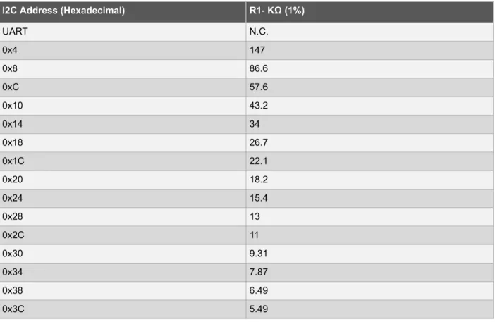
2C Address Selection
The choice of UART or I2C interface between the host CPU is made by applying a specific voltage level to pin #13
(I2C_ADDR_MEAS) on the PD39210. Additionally, the specific I2C address is also set by this voltage level. In all
cases, the voltage is set via an external resistor divider as shown in the following figure.
Figure 1-3. I2C Address Selection
The specific Value of R to choose UART or I2C and to set the address is given in the following table. Table 1-2. I2C Address Selection
I2C Address (Hexadecimal) R1- KΩ (1%)
UART N.C. 0x4 147 0x8 86.6 0xC 57.6 0x10 43.2 0x14 34 0x18 26.7 0x1C 22.1 0x20 18.2 0x24 15.4 0x28 13 0x2C 11 0x30 9.31 0x34 7.87 0x38 6.49 0x3C 5.49
Architecture
2.
Electrical Specifications
The following sections describe the electrical specifications for the PD39210 device.
2.1
Electrical Characteristics
For a complete list of electrical characteristics, see Microchip D21 Datasheet.
Table 2-1. General Operating Conditions
Symbol Parameter Conditions Min Typ Max Units
VDD Power supply voltage 3.0 3.3 3.63 V
VDDA Power supply voltage 3.0 3.3 3.63 V
TA Temperature range –40 25 85 °C
TJ Junction temperature 100 °C
2.2
Immunity
Table 2-2. Immunity
Symbol Parameter Conditions Min Max Units
ESD ESD rating HBM1 –2000 +2000 V
CDM2 –500 +500 V
1. ESD HBM complies with JESD22 Class 2 standard. 2. ESD CDM complies with JESD22 Class 1 standard.
2.3
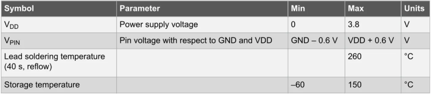
Absolute Maximum Ratings
Stresses beyond those listed in this section may cause permanent damage to the device. This is a stress rating only and functional operation of the device at these or other conditions beyond those indicated in the operational sections of this specification is not implied. Exposure to absolute maximum rating conditions for extended periods may affect device reliability.
Table 2-3. Absolute Maximum Ratings
Symbol Parameter Min Max Units
VDD Power supply voltage 0 3.8 V
VPIN Pin voltage with respect to GND and VDD GND – 0.6 V VDD + 0.6 V V
Lead soldering temperature (40 s, reflow)
260 °C
Storage temperature –60 150 °C
3.
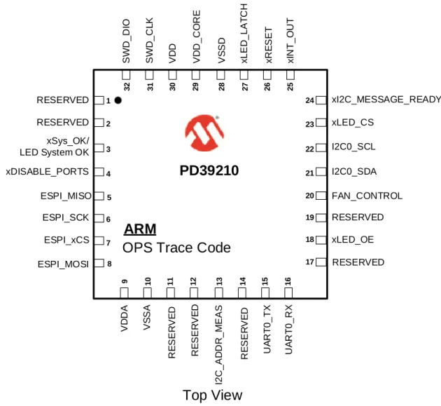
Pins
The PD39210 controller has 32 pins, which are described in this section.
3.1
Pin Diagrams
The following figures represent the top view of PD39210 device.
Figure 3-1. PD39210 Pin Diagram
PD39210
Top View
OPS Trace Code
24 23 22 21 19 20 18 17 FAN_CONTROL RESERVED I2C0_SCL I2C0_SDA xI2C_MESSAGE_READY xLED_CS xLED_OE RESERVED 13 14 15 16 11 10 12 9 I2C _A D D R _ M E A S V D D A V S S A R E S E R V E D R E S E R V E D R E S E R V E D U A R T 0_ RX U A R T 0_ TX 28 27 26 25 30 31 29 32 V S S D S W D _ D IO S W D _ C L K V D D V D D _ C O R E xL E D _ L A T C H xI N T _ O U T xR E S E T ESPI_MISO ESPI_SCK xSys_OK/ LED System OK xDISABLE_PORTS RESERVED ESPI_xCS ESPI_MOSI 1 2 3 4 6 5 7 8
ARM
RESERVEDNote: For definitions about markings in the pinout diagram, see Ordering Information.
3.2
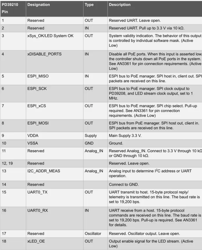
Pin Descriptions
The following tables describe the functional pin descriptions of the PD39210 device.
Table 3-1. Pin Descriptions
PD39210 Pin
Designation Type Description
1 Reserved OUT Reserved UART. Leave open.
2 Reserved IN Reserved UART. Pull up to 3.3 V via 10 kΩ.
3 xSys_OK/LED System OK OUT System validity indication. The behavior of this output is controlled by individual software mask. (Active Low)
4 xDISABLE_PORTS IN Disable all PoE ports. When this input is asserted low,
the controller shuts down all PoE ports in the system. See AN3361 for pin connection requirements. (Active Low)
5 ESPI_MISO IN ESPI bus to PoE manager. SPI host in, client out. SPI
packets are received on this line.
6 ESPI_SCK OUT ESPI bus to PoE manager. SPI clock output to
PD39208, and LED stream clock output, set to 1 MHz.
7 ESPI_xCS OUT ESPI bus to PoE manager. SPI chip select. Pull-up
required. See AN3361 for pin connection requirements. (Active Low)
8 ESPI_MOSI OUT ESPI bus from PoE manager. SPI host out, client in.
SPI packets are received on this line.
9 VDDA Supply Main Supply 3.3 V.
10 VSSA GND Ground.
11 Reserved Analog_IN Reserved Analog_IN. Connect to 3.3 V through 10 kΩ
or GND through 10 kΩ.
12, 19 Reserved Reserved. Leave open.
13 I2C_ADDR_MEAS Analog_IN Analog input to determine I2C address or UART
operation.
14 Reserved Connect to GND.
15 UART0_TX OUT UART transmit to host. 15-byte protocol reply/
telemetry is transmitted on this line. The baud rate is set to 19,200 bps.
16 UART0_RX IN UART receive from a host. 15-byte protocol
commands are received on this line. The baud rate is set to 19,200 bps. Pull-up is required. See AN3361 for details.
17 Reserved Oscillator Reserved. Oscillator output. Leave open.
18 xLED_OE OUT Output enable signal for the LED stream. (Active
Low)
...continued
PD39210 Pin
Designation Type Description
20 FAN_CONTROL OUT Logic out that may be used to control a fan driver.
(Active High)
21 I2C0_SDA IN/OUT I2C bidirectional data. 15-byte protocol messages are
transmitted on this line.
22 I2C0_SCL IN/OUT I2C clock from the host. Speed is limited to 400 KHz.
Clock stretch required. Pull up required, see AN3361 for details.
23 xLED_CS OUT Chip select signal for LED stream. (Active Low)
24 xI2C_MESSAGE_READY OUT I2C message ready for reading by the host. Controller
asserts this line low when it has an answer to the host. Therefore, the host can poll this line and initiate I2C read cycle only when the message is ready. After
the host reads the data from the controller, this pin is asserted to high. (Active Low)
25 xINT_OUT OUT Interrupt output indication. This line is asserted low
when a pre-configured event is in progress. (Active Low)
26 xRESET IN/OUT Host Reset input (Active Low). Controller can
generate self-reset. In this case, the xRESET pin is driven low by the controller for 100 µs. See AN3361 for pin connection requirements.
27 xLED_LATCH OUT Latch signal for LED stream. (Active Low)
28 VSSD GND Ground.
29 VDD_CORE Power 1.2 V core voltage connect 1 μF capacitor to VSSD.
30 VDD Supply Main 3.3 V supply.
31 SWD_CLK PD69210 and PD39210 use a 1 kΩ pull-up to 3.3 V.
PD69220 leave open or use 1k pull-up.
32 SWD_DIO Leave open.
ePAD ePAD Connect to VSSA. Must have sufficient copper mass
to ensure adequate thermal performance.
4.
Package Information
This section provides the package information for the PD39210 device.
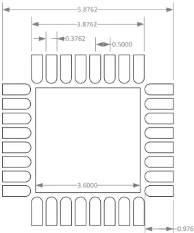
4.1
PD39210 Package Outline Drawing
The following figure shows the package drawing of PD39210 devices.
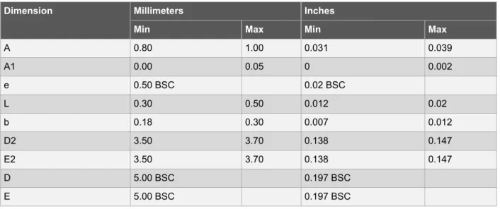
Figure 4-1. PD39210 Package Outline Drawing (32-Pin QFN 5 mm × 5 mm)
The following table lists the dimensions and measurements of the PD39210 package.
Table 4-1. PD39210 Package Outline Dimensions and Measurements
Dimension Millimeters Inches
Min Max Min Max
A 0.80 1.00 0.031 0.039 A1 0.00 0.05 0 0.002 e 0.50 BSC 0.02 BSC L 0.30 0.50 0.012 0.02 b 0.18 0.30 0.007 0.012 D2 3.50 3.70 0.138 0.147 E2 3.50 3.70 0.138 0.147 D 5.00 BSC 0.197 BSC E 5.00 BSC 0.197 BSC
Note: Dimensions do not include protrusions; they should not exceed 0.155 mm (0.006 in.) on any side. Lead dimension should not include solder coverage. Dimensions are in millimeters and inches for reference.
4.2
Thermal Specifications
The following table lists the thermal specifications of the PD39210.
Table 4-2. Thermal Specifications
Thermal Resistance Typ Units Description
θJA 40.9 °C/W Junction-to-ambient thermal resistance.
θJC 15.2 °C/W Junction-to-case thermal resistance.
4.3
Recommended PCB Layout
The following figures show the recommended PCB layout pattern for the 32-pin QFN 5 mm × 5 mm PD39210. Units are in mm.
Figure 4-2. Solder Mask
0.3762 0.5000 3.8762 5.8762 0.9762 3.6000
Package Information
Figure 4-3. Top-Layer Copper PCB Layout 0.30 5.80 0.90 3.50 3.80 0.50
Figure 4-4. Paste Mask
0.23 5.38
0.66 14.53 33.00
under the QFN package using any method they deem appropriate. Any design should be subject to system validation and qualification prior to commitment to mass production of field deployment. Use a 5 mil stencil.
4.4
Recommended Solder Reflow Information
RoHS 6/6
Pb-free 100% Matte Tin Finish
Package Peak Temperature for Solder Reflow (40 s maximum exposure)—260 °C (0 °C, –5 °C)
Table 4-3. Classification Reflow Profiles
Profile Feature Sn-Pb Eutectic Assembly Pb-Free Assembly
Average ramp-up rate (TSmax to Tp) 3 °C/second max 3 °C/second max
Preheat
Temperature min (TSmin) 100 °C 150 °C
Temperature max (TSmax) 150 °C 200 °C
Time (tsmin to tsmax) 60 s to 120 s 60 s to 180 s
Time Maintained
Temperature (TL) 183 °C 217 °C
Time (tL) 60 s to 150 s 60 s to 150 s
Peak classification temperature (TP) 210 °C to 235 °C 240 °C to 255 °C
Time within 5 °C of actual peak temperature (tp)
10 s to 30 s 20 s to 40 s
Ramp-down rate 6 °C/second max 6 °C/second max
Time 25 °C to peak temperature 6 minutes max 8 minutes max
Figure 4-5. Classification Reflow Profiles
Table 4-4. Pb-Free Process—Package Classification Reflow Temperatures
Package Thickness Volume <350 mm3 Volume 350–2000 mm3 Volume >2000 mm3
Less than 1.6 mm1 260 + 0 °C 260 + 0 °C 260 + 0 °C
...continued
Package Thickness Volume <350 mm3 Volume 350–2000 mm3 Volume >2000 mm3
1.6 mm to 2.5 mm1 260 + 0 °C 250 + 0 °C 245 + 0 °C
Greater than or equal to
2.5 mm1 250 + 0 °C 245 + 0 °C 245 + 0 °C
1. Tolerance: The device manufacturer or supplier should assure process compatibility up to and including the stated classification temperature, meaning that the peak reflow temperature is +0 °C. For example, 260 °C to 0 °C, at the rated MSL value.
Note: Exceeding the ratings that are mentioned in the preceding table might cause damage to the device.
4.5
Reference Documents
• PD39210 Serial Communication Protocol User Guide
• Microchip AN3361 Designing an IEEE 802.3af/802.3at/802.3bt-Compliant PD69208 48-Port PoE System • Microchip Designing an IEEE 802.3af/802.3at-Compliant PD39208 48-Port PoE System
• AN3378 Surge Protection Application Note 8-Port PSE PoE Manager PD69208T4/M/4T4 • PD692x0+PD69208M/208T4/204T4 Implementing Perpetual PoE (PPoE) and Fast PoE • PD69210, PD69220 PoE PSE Controller Datasheet
• PD69200 PoE PSE Controller Datasheet • PD39208 PoE PSE Manager Datasheet
5.
Ordering Information
The following table lists the part ordering information for the PD39210 device.
Table 5-1. Ordering Information
Part Number Package Packaging Type
Temperature Part Marking Tray Marking
PD39210D1VVVV2SS3 Plastic QFN
5 mm × 5 mm (32 lead)
Tray –40 °C to 85 °C Microchip Logo
PD39210 ARM Logo YY4 WW5 NNN6 PD39210D-VVVVSS PD-OOOOGabb7 YYWW PD39210D1VVVV2SS3-TR Plastic QFN 5 mm × 5 mm (32 lead)
Tape and reel –40 °C to 85 °C Microchip Logo PD39210 ARM Logo YY4 WW5 NNN6
1. D is detection method.
– C= IEEE 802.3 and pre-standard – R= IEEE 802.3
2. VVVV is firmware revision.
3. SS is firmware parameters options. 4. Year code (last two digits of calendar year). 5. Week code (week of January 1 is week 01). 6. Alphanumeric trace code.
7. Optional part number.
The firmware release note has all required information about how to specify the choice of VVVV and SS. Find the Firmware Release Notes in the Microchip Software Libraries, and register to My Microchip account to access the release notes.
Note: The package meets RoHS, Pb-free of the European Council to minimize the environmental impact of electrical equipment.
Note: Initial burning of controller's firmware is performed in the factory. Firmware upgrades can be performed by users using the communication interface. For more information, see TN-140 (Catalog Number: 06-0024-081).
6.
Revision History
Revision Date Description
C 12/2020 • Replaced the figures in 4.3 Recommended PCB Layout with three new images. B 09/2020 • Added "R= IEEE 802.3" to Ordering Information.
A 07/2020 This is the initial issue of this document. The PD39210 PoE PSE controller is a new product offering and has not been previously described in any other document. The PD39210 PoE PSE controller was previously described in the following documents:
• PD69208T4 and PD69210 Datasheet (Revision 3 September 2019 Document Number PD-000357193)
• PD69204T4 and PD69210 Datasheet (Revision 3 September 2019 Document Number PD-000359832)
• PD69208M and PD69210 Datasheet (Revision 3 September 2019 Document Number PD-000359833)
The Microchip Website
Microchip provides online support via our website at www.microchip.com/. This website is used to make files and information easily available to customers. Some of the content available includes:
• Product Support – Data sheets and errata, application notes and sample programs, design resources, user’s guides and hardware support documents, latest software releases and archived software
• General Technical Support – Frequently Asked Questions (FAQs), technical support requests, online discussion groups, Microchip design partner program member listing
• Business of Microchip – Product selector and ordering guides, latest Microchip press releases, listing of seminars and events, listings of Microchip sales offices, distributors and factory representatives
Product Change Notification Service
Microchip’s product change notification service helps keep customers current on Microchip products. Subscribers will receive email notification whenever there are changes, updates, revisions or errata related to a specified product family or development tool of interest.
To register, go to www.microchip.com/pcn and follow the registration instructions.
Customer Support
Users of Microchip products can receive assistance through several channels: • Distributor or Representative
• Local Sales Office
• Embedded Solutions Engineer (ESE) • Technical Support
Customers should contact their distributor, representative or ESE for support. Local sales offices are also available to help customers. A listing of sales offices and locations is included in this document.
Technical support is available through the website at: www.microchip.com/support
Microchip Devices Code Protection Feature
Note the following details of the code protection feature on Microchip devices:• Microchip products meet the specifications contained in their particular Microchip Data Sheet.
• Microchip believes that its family of products is secure when used in the intended manner and under normal conditions.
• There are dishonest and possibly illegal methods being used in attempts to breach the code protection features of the Microchip devices. We believe that these methods require using the Microchip products in a manner outside the operating specifications contained in Microchip’s Data Sheets. Attempts to breach these code protection features, most likely, cannot be accomplished without violating Microchip’s intellectual property rights. • Microchip is willing to work with any customer who is concerned about the integrity of its code.
• Neither Microchip nor any other semiconductor manufacturer can guarantee the security of its code. Code protection does not mean that we are guaranteeing the product is “unbreakable.” Code protection is constantly evolving. We at Microchip are committed to continuously improving the code protection features of our products. Attempts to break Microchip’s code protection feature may be a violation of the Digital Millennium Copyright Act. If such acts allow unauthorized access to your software or other copyrighted work, you may have a right to sue
Legal Notice
Information contained in this publication is provided for the sole purpose of designing with and using Microchip products. Information regarding device applications and the like is provided only for your convenience and may be superseded by updates. It is your responsibility to ensure that your application meets with your specifications. THIS INFORMATION IS PROVIDED BY MICROCHIP “AS IS”. MICROCHIP MAKES NO REPRESENTATIONS OR WARRANTIES OF ANY KIND WHETHER EXPRESS OR IMPLIED, WRITTEN OR ORAL, STATUTORY OR OTHERWISE, RELATED TO THE INFORMATION INCLUDING BUT NOT LIMITED TO ANY IMPLIED
WARRANTIES OF NON-INFRINGEMENT, MERCHANTABILITY, AND FITNESS FOR A PARTICULAR PURPOSE OR WARRANTIES RELATED TO ITS CONDITION, QUALITY, OR PERFORMANCE.
IN NO EVENT WILL MICROCHIP BE LIABLE FOR ANY INDIRECT, SPECIAL, PUNITIVE, INCIDENTAL OR CONSEQUENTIAL LOSS, DAMAGE, COST OR EXPENSE OF ANY KIND WHATSOEVER RELATED TO THE INFORMATION OR ITS USE, HOWEVER CAUSED, EVEN IF MICROCHIP HAS BEEN ADVISED OF THE POSSIBILITY OR THE DAMAGES ARE FORESEEABLE. TO THE FULLEST EXTENT ALLOWED BY LAW, MICROCHIP'S TOTAL LIABILITY ON ALL CLAIMS IN ANY WAY RELATED TO THE INFORMATION OR ITS USE WILL NOT EXCEED THE AMOUNT OF FEES, IF ANY, THAT YOU HAVE PAID DIRECTLY TO MICROCHIP FOR THE INFORMATION. Use of Microchip devices in life support and/or safety applications is entirely at the buyer’s risk, and the buyer agrees to defend, indemnify and hold harmless Microchip from any and all damages, claims, suits, or expenses resulting from such use. No licenses are conveyed, implicitly or otherwise, under any Microchip intellectual property rights unless otherwise stated.
Trademarks
The Microchip name and logo, the Microchip logo, Adaptec, AnyRate, AVR, AVR logo, AVR Freaks, BesTime, BitCloud, chipKIT, chipKIT logo, CryptoMemory, CryptoRF, dsPIC, FlashFlex, flexPWR, HELDO, IGLOO, JukeBlox, KeeLoq, Kleer, LANCheck, LinkMD, maXStylus, maXTouch, MediaLB, megaAVR, Microsemi, Microsemi logo, MOST, MOST logo, MPLAB, OptoLyzer, PackeTime, PIC, picoPower, PICSTART, PIC32 logo, PolarFire, Prochip Designer, QTouch, SAM-BA, SenGenuity, SpyNIC, SST, SST Logo, SuperFlash, Symmetricom, SyncServer, Tachyon,
TempTrackr, TimeSource, tinyAVR, UNI/O, Vectron, and XMEGA are registered trademarks of Microchip Technology Incorporated in the U.S.A. and other countries.
APT, ClockWorks, The Embedded Control Solutions Company, EtherSynch, FlashTec, Hyper Speed Control, HyperLight Load, IntelliMOS, Libero, motorBench, mTouch, Powermite 3, Precision Edge, ProASIC, ProASIC Plus, ProASIC Plus logo, Quiet-Wire, SmartFusion, SyncWorld, Temux, TimeCesium, TimeHub, TimePictra, TimeProvider, Vite, WinPath, and ZL are registered trademarks of Microchip Technology Incorporated in the U.S.A.
Adjacent Key Suppression, AKS, Analog-for-the-Digital Age, Any Capacitor, AnyIn, AnyOut, BlueSky, BodyCom, CodeGuard, CryptoAuthentication, CryptoAutomotive, CryptoCompanion, CryptoController, dsPICDEM,
dsPICDEM.net, Dynamic Average Matching, DAM, ECAN, EtherGREEN, In-Circuit Serial Programming, ICSP, INICnet, Inter-Chip Connectivity, JitterBlocker, KleerNet, KleerNet logo, memBrain, Mindi, MiWi, MPASM, MPF, MPLAB Certified logo, MPLIB, MPLINK, MultiTRAK, NetDetach, Omniscient Code Generation, PICDEM,
PICDEM.net, PICkit, PICtail, PowerSmart, PureSilicon, QMatrix, REAL ICE, Ripple Blocker, SAM-ICE, Serial Quad I/O, SMART-I.S., SQI, SuperSwitcher, SuperSwitcher II, Total Endurance, TSHARC, USBCheck, VariSense,
ViewSpan, WiperLock, Wireless DNA, and ZENA are trademarks of Microchip Technology Incorporated in the U.S.A. and other countries.
SQTP is a service mark of Microchip Technology Incorporated in the U.S.A.
The Adaptec logo, Frequency on Demand, Silicon Storage Technology, and Symmcom are registered trademarks of Microchip Technology Inc. in other countries.
Quality Management System
AMERICAS ASIA/PACIFIC ASIA/PACIFIC EUROPE Corporate Office 2355 West Chandler Blvd. Chandler, AZ 85224-6199 Tel: 480-792-7200 Fax: 480-792-7277 Technical Support: www.microchip.com/support Web Address: www.microchip.com Atlanta Duluth, GA Tel: 678-957-9614 Fax: 678-957-1455 Austin, TX Tel: 512-257-3370 Boston Westborough, MA Tel: 774-760-0087 Fax: 774-760-0088 Chicago Itasca, IL Tel: 630-285-0071 Fax: 630-285-0075 Dallas Addison, TX Tel: 972-818-7423 Fax: 972-818-2924 Detroit Novi, MI Tel: 248-848-4000 Houston, TX Tel: 281-894-5983 Indianapolis Noblesville, IN Tel: 317-773-8323 Fax: 317-773-5453 Tel: 317-536-2380 Los Angeles Mission Viejo, CA Tel: 949-462-9523 Fax: 949-462-9608 Tel: 951-273-7800 Raleigh, NC Tel: 919-844-7510 New York, NY Tel: 631-435-6000 San Jose, CA Tel: 408-735-9110 Tel: 408-436-4270 Australia - Sydney Tel: 61-2-9868-6733 China - Beijing Tel: 86-10-8569-7000 China - Chengdu Tel: 86-28-8665-5511 China - Chongqing Tel: 86-23-8980-9588 China - Dongguan Tel: 86-769-8702-9880 China - Guangzhou Tel: 86-20-8755-8029 China - Hangzhou Tel: 86-571-8792-8115 China - Hong Kong SAR Tel: 852-2943-5100 China - Nanjing Tel: 86-25-8473-2460 China - Qingdao Tel: 86-532-8502-7355 China - Shanghai Tel: 86-21-3326-8000 China - Shenyang Tel: 86-24-2334-2829 China - Shenzhen Tel: 86-755-8864-2200 China - Suzhou Tel: 86-186-6233-1526 China - Wuhan Tel: 86-27-5980-5300 China - Xian Tel: 86-29-8833-7252 China - Xiamen Tel: 86-592-2388138 China - Zhuhai Tel: 86-756-3210040 India - Bangalore Tel: 91-80-3090-4444 India - New Delhi Tel: 91-11-4160-8631 India - Pune Tel: 91-20-4121-0141 Japan - Osaka Tel: 81-6-6152-7160 Japan - Tokyo Tel: 81-3-6880- 3770 Korea - Daegu Tel: 82-53-744-4301 Korea - Seoul Tel: 82-2-554-7200 Malaysia - Kuala Lumpur Tel: 60-3-7651-7906 Malaysia - Penang Tel: 60-4-227-8870 Philippines - Manila Tel: 63-2-634-9065 Singapore Tel: 65-6334-8870 Taiwan - Hsin Chu Tel: 886-3-577-8366 Taiwan - Kaohsiung Tel: 886-7-213-7830 Taiwan - Taipei Tel: 886-2-2508-8600 Thailand - Bangkok Tel: 66-2-694-1351 Vietnam - Ho Chi Minh Tel: 84-28-5448-2100 Austria - Wels Tel: 43-7242-2244-39 Fax: 43-7242-2244-393 Denmark - Copenhagen Tel: 45-4485-5910 Fax: 45-4485-2829 Finland - Espoo Tel: 358-9-4520-820 France - Paris Tel: 33-1-69-53-63-20 Fax: 33-1-69-30-90-79 Germany - Garching Tel: 49-8931-9700 Germany - Haan Tel: 49-2129-3766400 Germany - Heilbronn Tel: 49-7131-72400 Germany - Karlsruhe Tel: 49-721-625370 Germany - Munich Tel: 49-89-627-144-0 Fax: 49-89-627-144-44 Germany - Rosenheim Tel: 49-8031-354-560 Israel - Ra’anana Tel: 972-9-744-7705 Italy - Milan Tel: 39-0331-742611 Fax: 39-0331-466781 Italy - Padova Tel: 39-049-7625286 Netherlands - Drunen Tel: 31-416-690399 Fax: 31-416-690340 Norway - Trondheim Tel: 47-72884388 Poland - Warsaw Tel: 48-22-3325737 Romania - Bucharest Tel: 40-21-407-87-50 Spain - Madrid Tel: 34-91-708-08-90 Fax: 34-91-708-08-91 Sweden - Gothenberg Tel: 46-31-704-60-40 Sweden - Stockholm Tel: 46-8-5090-4654 UK - Wokingham Tel: 44-118-921-5800