U
niversit
at
¨
A
ugsburg
The Model of Computation of CUDA and
its Formal Semantics
Based on the Master’s Thesis of Axel Habermaier
Axel Habermaier
Report 2011-14 October 2011
I
nstitut f
ur
¨
I
nformatik
Copyright c Axel Habermaier Institut für Informatik Universität Augsburg
D–86135 Augsburg, Germany
http://www.Informatik.Uni-Augsburg.DE — all rights reserved —
Abstract
We formalize the model of computation of modern graphics cards based on the specification of Nvidia’s Compute Unified Device Architecture (CUDA). CUDA programs are executed by thousands of threads concurrently and have access to several different types of memory with unique access patterns and latencies. The underlying hardware uses a single instruction, multiple threads execution model that groups threads into warps. All threads of the same warp execute the program in lockstep. If threads of the same warp execute a data-dependent control flow instruction, control flow might diverge and the different execution paths are executed sequentially. Once all paths complete execution, all threads are executed in parallel again. An operational semantics of a significant subset of CUDA’s memory operations and programming instructions is presented, including shared and non-shared memory opera-tions, atomic operations on shared memory, cached memory access, recursive function calls, control flow instructions, and thread synchronization.
Based on this formalization we prove that CUDA’s single instruction, multiple threads execution model is safe: For all threads it is provably true that a thread only executes the instructions it is allowed to execute, that it does not continue execution after processing the last instruction of the program, and that it does not skip any instructions it should have executed. On the other hand, we demonstrate that CUDA’s inability to handle control flow instructions individually for each thread can cause unexpected program behavior in the sense that a liveness property is violated.
Contents
1 Introduction 4
2 Overview of CUDA 7
2.1 Evolution of GPUs . . . 7
2.2 Architecture of a Modern GPU . . . 9
2.2.1 Chip Layout . . . 10
2.2.2 Processing Units . . . 11
2.2.3 Memories and Caches . . . 13
2.2.4 Compute Capability . . . 14 2.3 CUDA Programs . . . 15 2.3.1 Thread Organization . . . 17 2.3.2 Memory Types . . . 18 2.3.3 Introduction to PTX . . . 21 2.3.4 Compilation Infrastructure . . . 23 2.4 Alternatives to CUDA . . . 24 2.4.1 OpenCL . . . 24 2.4.2 Direct Compute . . . 25
3 Conventions, Global Constants, and Rules 27 3.1 Conventions . . . 27
3.2 Global Constants . . . 29
3.3 Rules . . . 29
4 Formal Memory Model 32 4.1 Overview of Memory Programs . . . 34
4.2 Formalization of Caches . . . 35
4.2.1 Cache Lines . . . 36
4.2.2 Cache Operations . . . 37
4.3 Formalization of the Memory Environment . . . 42
4.4 Formalization and Formal Semantics of Memory Programs . . . 45
4.4.1 Implicit Program State . . . 46
4.4.2 Boolean Expressions . . . 48
4.4.3 Operational Expressions . . . 49
4.4.4 Program Statements . . . 54
4.5 Memory Operation Semantics . . . 56
5 Formal Semantics of CUDA’s Model of Computation 64
5.1 Formalization of PTX . . . 64
5.1.1 PTX Instructions and Features Included in the Formalization . . . 65
5.1.2 Definition of Program Environments . . . 67
5.1.3 Representation of PTX Programs as Program Environments . . . 70
5.2 Expression Semantics . . . 76
5.3 Thread Semantics . . . 78
5.3.1 Thread Actions . . . 79
5.3.2 Thread Rules . . . 81
5.3.3 Conditional Thread Execution . . . 84
5.4 Warp Semantics . . . 85
5.4.1 Formalization of the Branching Algorithm . . . 86
5.4.2 Formalization of Votes and Barriers . . . 99
5.4.3 Warp Rules . . . 100
5.5 Thread Block Semantics . . . 101
5.5.1 Formalization of the Thread Block Synchronization Mechanism . . . . 103
5.5.2 Thread Block Rules . . . 107
5.6 Grid Semantics . . . 108
5.7 Context Semantics . . . 110
5.7.1 Formalization of Warp, Thread Block, and Grid Scheduling . . . 110
5.7.2 Context Input/Output . . . 112
5.7.3 Context Rules . . . 113
5.8 Device Semantics . . . 115
5.8.1 Linking the Program Semantics to the Memory Environment . . . 115
5.8.2 Device Input/Output . . . 116
5.8.3 Device Rules . . . 118
5.9 Summary . . . 120
6 Correctness of the Branching Algorithm 121 6.1 Implications of Warp Level Branching . . . 121
6.2 Control Flow Consistency . . . 123
6.3 Single Warp Semantics . . . 125
6.3.1 Modified Thread Rules . . . 125
6.3.2 Modified Warp Rules . . . 127
6.4 Proof of the Safety Property . . . 130
6.5 Formalization of the Liveness Property . . . 140
6.6 Summary . . . 141 7 Conclusion 142 List of Symbols 145 List of Listings 146 List of Figures 147 Bibliography 148
1 Introduction
Stanford University’s Folding@Home1 is a distributed computing application designed to study protein folding and protein folding diseases. With more than 70 peer-reviewed papers2, the project’s aim is to help form a better understanding of the protein folding process and related diseases including Alzheimer’s disease, Parkinson’s disease, and many forms of Cancer. Even though some proteins fold in only a millionth of a second, computer simulations of protein folding are extremely slow, taking years in some cases3. Being so computationally demanding, the Folding@Home project distributes the necessary calculations to thousands of client computers. People from around the world support the project by downloading the client and donating their idle CPU time to the project. Additionally, in recent years people have been able to run the client on their graphics card as well, resulting in a significant increase in computational power devoted to Folding@Home. All in all, the computational resources available to the project have already crossed the peta FLOPS barrier.
Since the molecular dynamics simulations performed by the Folding@Home client are computationally expensive, running them on GPUs has the potential of drastically reducing computation times. With the advent of general purpose GPU programming supported by both Nvidia and AMD graphics cards, it has become viable to develop new Folding@Home clients that run the computations on the GPU instead of the CPU. The results speak for themselves: The GPU clients outperform their CPU counterparts by at least two orders of magnitude, even though the peak theoretical power of the GPUs has not yet been reached, i.e. further optimizations are still possible. Additionally, many molecules simulated by the CPU client are too small to fully utilize the graphics card because of its massively parallel nature. Therefore, it is expected that the performance gap between CPUs and GPUs will increase even further for simulations of larger molecules [1]. But even today GPUs already play an important role for Folding@Home as illustrated by figure 1.1. Even though the number of active GPUs contributing to the project is way smaller than the amount of CPUs, the actual floating point operations per second exceed those of the CPUs by an order of magnitude. The same applies to the PlayStation 3, which runs a special client optimized for the console’s Cell chip.
Platform TFLOPS Active Processors
CPUs (Windows) 213 223933
AMD GPUs 697 6481
Nvidia GPUs 2199 8760
PlayStation 3 1671 28090
Figure 1.1: Folding@Home Client Statistics4
1http://folding.stanford.edu/
2http://folding.stanford.edu/English/Papers, last access 2010-10-28 3http://folding.stanford.edu/English/Science, last access 2010-10-28
4based onhttp://fah-web.stanford.edu/cgi-bin/main.py?qtype=osstats, last access 2010-10-28; see also http://folding.stanford.edu/English/FAQ-flops
Figure 1.2: Screenshot of the Folding@Home Client for Nvidia GPUs
There are some issues, however, that the GPU client has to deal with. As general purpose GPU programming has only been recently introduced, development tools and environments are not yet as mature as their CPU counterparts. Additionally, GPU programming is still very close to the hardware, so problems like efficient memory accesses, CPU/GPU synchro-nization, and divergent control flow must be considered carefully. Precision of floating point operations is an important issue too, as using double precision computations instead of single precision ones is significantly slower on today’s GPUs.
Another area where GPUs excel is the reconstruction phase of magnetic resonance imaging. There, the data sampled by a scanner needs to be transformed into an image that is then presented to a human for further analysis. Again, a speedup of two orders of magnitude can be achieved by offloading the required transformations to the GPU. As [2, 8] shows, hardware-specific optimizations are of utmost importance, though: A naive implementation is only about ten times faster then the equivalent CPU program. However, once memory accesses are optimized and the hardware’s trigonometry function units are fully utilized, GPUs outperform CPUs by a factor of about 100 in total and one specific sub-problem is even computed around 357 times faster.
Figure 1.3: MRI Scan of a Human Head5
As these two examples show, GPUs can significantly speed up certain algorithms and operations — provided that they suit the novel model of computation of GPUs which vastly
differs from the traditional one of x86 CPUs. Because of those tremendous performance improvements, Folding@Home will most likely continue to focus on the development of the GPU clients. But besides Folding@Home, there are many other research projects in physics, chemistry, biology, and other sciences that benefit significantly from GPU-accelerated compu-tations. On the other hand, GPUs are also used outside academia in real-world applications where they might affect people’s life or health as the aforementioned MRI example illustrates. Thus, developers of such applications must be able to guarantee that their programs behave correctly in all cases — either by extensive testing or by formally proving certain properties of their programs. However, general purpose GPU programming is a novel field of research and academic interest is mostly focused on finding ways to adapt specific problems and algorithms to the GPU’s programming model and on optimizing GPU programs in order to make the computations as efficient as possible. Correctness, on the other hand, is only of secondary interest and is not proven formally in most cases. By contrast, this report is aimed at formalizing the model of computation of CUDA, Nvidia’s general purpose GPU programming infrastructure. With some further work that is outside the scope of this re-port, it should be possible to use the presented formalization to formally prove properties of GPU-accelerated programs.
Based on an informal overview of the hardware architecture and the programming model in chapter 2, CUDA’s memory model and program semantics are formalized in chapters 4 and 5, respectively. Although the formalization is not exhaustive, it includes most of the important features and instructions supported by CUDA, like cached memory operations, thread synchronization, thread divergence caused by data-dependant control flow instruc-tions, atomic memory operainstruc-tions, and many more. Due to the complexity of the underlying hardware and CUDA, contrasting GPU and CPU semantics as a whole is outside the scope of this report. However, chapter 6 indeed shows a difference in program behavior caused by the GPU’s single instruction, multiple thread (SIMT) architecture. While in real-world scenarios mostly relevant for optimal performance, the SIMT architecture might cause deadlocks that would not occur if the program were executed on the CPU. We show that only terminating programs are provably correct in the general case.
2 Overview of CUDA
Compared to traditional x86 CPUs, CUDA utilizes a different programming model to take advantage of the massively parallel nature of modern GPUs. CUDA programs are concur-rently executed by thousands of threads in parallel and have access to a variety of different memory types, all of which have distinct access characteristics, sizes, and uses. Unlike x86 CPUs, GPUs do not execute each thread individually, but rather group threads into warps. These warps are executed individually, but all threads of the same warp execute their in-structions in lockstep. If the control flow of threads of the same warp diverges due to a data-dependant conditional branch instruction, execution of the warp is serialized for each unique path, disabling the threads that did not take the path. When all paths complete, the threads converge back to the same path and they execute concurrently in lockstep again.
With the first release of CUDA as recently as November 2006 [3], the programming model is still very close to the hardware. Therefore, CUDA developers must take into account the distinctive traits and feature sets of the hardware for a program to run as efficiently as possible on the GPU. While efficiency and performance are not the primary topic of this report, the formalization of the semantics is indeed affected by the novelty of general purpose GPU programming; we generally define the semantics in a low-level fashion and often refer to the hardware implementation of a specific feature. As GPUs have just recently gained features such as indirect function calls, recursion and dynamic memory allocation, it will probably take several years before high-level abstractions like virtual machines similar to Java will become viable from a performance standpoint. At that point, it should be possible to define a formal semantics that is less closely tied to the underlying hardware.
Since the hardware is such an integral part of CUDA, we first take a brief look at the architecture of modern GPUs before we give an overview of CUDA’s programming model. As the primary use of modern GPUs is still the acceleration of graphics rendering, we explain the evolution of CUDA based on the evolution of the underlying hardware from fixed-function graphics co-processors to fully programmable general purpose processors. In this chapter, we also introduce the programming languages and compiler infrastructure used to develop CUDA applications and also outline some of the differences and similarities of CUDA compared to other general purpose GPU programming frameworks. Except for section 2.4, this entire report focuses on Nvidia’s GPUs, as CUDA is a Nvidia exclusive technology. We focus on CUDA instead of multi-vendor frameworks such as OpenCL and Direct Compute because CUDA’s specification was the most comprehensive one at the time of writing.
2.1 Evolution of GPUs
In the late 1990s, GPUs were used exclusively to accelerate fixed-function graphics pro-cessing. Using an API like OpenGL or Direct3D, a developer instructed the GPU to draw triangles on the screen, using a combination of different states to specify how the triangles
should be textured, lit, alpha-blended, etc. At that time, developers were only able to use the functionality that was supported by the hardware and exposed by the graphics API; programming the GPU directly was not yet possible.
Having only a limited instruction set and no programmability was the main reason why the GPUs of that time outperformed the CPUs: The chip developers were able to use the chip’s transistor budget to implement slow operations like texture filtering and raster operations in hardware, as they did not have to implement transistor-heavy functionality like data caches and branch prediction logic. Furthermore, graphics rendering is an inherently parallel task; each vertex of a geometry set and each rasterized pixel can be processed independently and in parallel. This allowed the GPUs to increase the performance by just putting more of the same functional units on the chip.
Eventually, it became apparent that the fixed-function design severely limited the graphi-cal effects that can be achieved by GPU based renderers. In 2001, Nvidia introduced a new generation of graphics processors which for the first time allowed the GPU to be programmed directly by the developer. The new programmability could be used to specify shader pro-grams that operated on individual vertices and pixels, however, shaders had to be very short and control flow instructions were missing.
Over time, GPUs became faster by allowing more shaders to be executed in parallel, while at the same time increasing the instruction count limit and adding new operations to the instruction set. At the same time, both OpenGL and Direct3D introduced the C-like languages GLSL and HLSL respectively which could be used to develop shaders in a more higher-level fashion than writing assembly code.
With the DirectX 10 generation of graphics card, GPUs gained the ability to be used for general purpose processing, circumventing the traditional graphics APIs thanks to the introduction of CUDA (Nvidia) and CAL (AMD). Previously, some developers had already attempted to use GPUs for non-graphics related tasks, but had to fit their algorithms into the limits imposed by the graphics APIs. As those were not designed for such usage, the developers had to work around the limitations of both the API and the hardware, reducing the possible performance gains. Another important change of the DirectX 10 generation of GPUs was the introduction of unified shading. Previous generations of graphics card had distinct hardware units for vertex and pixel shaders. That was problematic in some cases; for example if a draw operation was heavily pixel shader bound, the vertex shader parts of the chip were running idle. As DirectX 10 added yet another type of shader, the geometry shader, the traditional design of the shader units would have become too wasteful. Therefore, all DirectX 10 chips consist of unified shading units, allowing the same hardware units to be used to execute vertex, geometry, and pixel shaders. For general purpose programming, this meant that a program was now able to use all hardware units available on the graphics card. Still not usable are some of the fixed-function units that are still needed for performance reasons; those remain idle when the chip executes a non-graphics program. Future generations of graphics cards will probably replace more and more of the current fixed-function functionality by programmable units that then might be usable by non-graphics related programs as well.
With CUDA, developers were now able to write general purpose applications without having to pay attention to the graphics heritage of the GPUs. Additionally, Nvidia added dedicated functionality to the chips which — until now — are only relevant to general purpose programming, like shared and non-shared read- and writable memory, atomic memory operations, and explicit synchronization points. The DirectX 11 generation added even more features like recursion, a cache hierarchy for improved latency, indirect function
calls, and more. All of these features are exposed directly to the developers who can use, for example, an extended version of C to program the GPU [2, 2]. Some of these features, especially indirect function calls, are likely to be supported by future versions of the shader programming languages as well. DirectX 11, for instance, has already added support for interfaces and classes to HLSL, although currently calls to an interface function are not virtual but resolved at shader link time [4].
For the future, it is expected that the importance of graphics APIs will vanish whereas the general programmability APIs will gain more traction. Tim Sweeney, one of the developers of the successful Unreal Engine 3, is already predicting that they will write their next generation
renderer in a programming language such as C++ or CUDA, abandoning OpenGL and
Direct3D entirely1. Another possibility is to take a hybrid approach, where the graphics APIs are used for the basic rendering work and the greater flexibility of general purpose APIs is used to accelerate post-processing effects. For instance, there is already a game that use a compute shader, the DirectX 11 equivalent of a CUDA program, to calculate the screen space ambient occlusion effect for scenes rendered with a traditional renderer2.
2.2 Architecture of a Modern GPU
GPUs have both strengths and weaknesses compared to traditional (multi-core) CPUs. There-fore, it depends on the program whether it can take advantage of the GPU’s superior compu-tational power or whether it is actually faster to run it on the CPU. Because of their graphics acceleration heritage, GPUs specialize on highly parallel as well as compute and memory bandwidth intensive tasks, whereas CPUs excel at sequential, control flow intensive ones. Hence, GPUs have more computational power and bandwidth than the CPUs at the cost of an increased operation latency. This latency, however, can be completely hidden if the program being run is sufficiently parallel, i.e. a massive number of threads can be run concurrently, as explained later on.
While there are many different chips capable of executing CUDA applications, we focus on the latest generation of graphics cards called Fermi or GF100. The remainder of this section discusses those parts of Fermi’s architecture that influence the semantics of CUDA programs, leaving out all the complexities that are not relevant for this report. The figures below are simplified versions of figures found in [5] and [6]. Additional information about Fermi’s architecture can be found in [5], [7], [3], [8], [9], [6], and [2]3.
Fermi is Nvidia’s current high-end chip and has — like all recent graphics chips — a modular design: With relatively low engineering effort, performance, mainstream and low-end chips can be derived from the top model, offering less features and performance at a lower price point. All of these GPUs use the same basic architecture and only differ in memory sizes and the number of functional units still left in the chip. Thus, when we speak of the “Fermi architecture”, we actually mean the basic architecture described below, parameterized over the memory sizes and the number of functional units. For a better understanding, the following sections and figures use the concrete values of the high-end chip GF100 instead of abstract placeholders. Later, we do indeed use global constants to
1http://arstechnica.com/gaming/news/2008/09/gpu-sweeney-interview.ars, last access 2010-10-10 2http://www.anandtech.com/show/2848/2, last access 2010-10-10
3Unless noted otherwise, all referenced Nvidia documents can be found athttp://developer.nvidia.com/
parameterize the domains and functions, as we want the semantics to be applicable to all Fermi-based GPUs.
2.2.1 Chip Layout
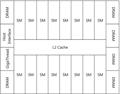
Figure 2.1: Fermi Chip Layout
Figure 2.1 gives an overview of Fermi’s basic chip layout. The GPU has six memory partitions positioned around a central L2 cache. Fermi supports cached read and write access to shared and non-shared memory as well as atomic and volatile memory operations. Section 2.2.3 takes a closer look at the different kinds of memory found on a Fermi chip.
The GPU uses the host interface for all communications with the CPU. The CPU has read and write access to the GPU’s memory, loads CUDA program code onto the GPU and launches programs on the GPU with a given set of input parameters. Once the program has been completed, the CPU is informed that the output produced by the program is ready for consumption by the host program. The communication between the CPU and GPU can be complex as both processors operate independently and in parallel. It is the graphics driver’s responsibility to synchronize both processors when specific events occur. We do not go into further details concerning the interaction of CPUs and GPUs and also do not consider multi-GPU setups.
The Giga Thread scheduler is responsible for distributing waiting threads to the 16 stream-ing multiprocessors (SM). The schedulstream-ing algorithm used by the scheduler is unknown. A SM executes many threads in parallel and issues read and write requests to the L2 cache or directly to the DRAM. The architecture of SMs is explained in further detail in section 2.2.2.
As mentioned above, Fermi’s architecture was designed to be flexible, such that parts of the chip can be easily removed to produce cheaper and smaller chips. This is achieved by reducing the L2 cache size, the amount of DRAM partitions, and the number of SMs on the chip, as well as by removing other fixed-function, graphics-related functionality not shown in figure 2.1. In fact, for the first derivation of GF100, GF104, Nvidia also modified the SMs
in an attempt to improve graphics performance at the expense of reducing the performance of certain CUDA-exclusive features. The GF104 changes, however, only affect the number and capabilities of the computation units within the SMs and have therefore no direct effect on the semantics of CUDA programs.
2.2.2 Processing Units
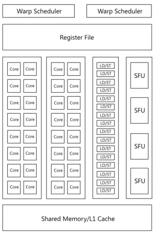
Figure 2.2: Fermi Streaming Multiprocessor
Each streaming multiprocessor can have up to a total of 1536 threads scheduled for exe-cution. The architecture used to manage such a large amount of threads is shown in figure 2.2.
Each SM consists of 32 CUDA cores capable of performing floating point and integer calculations. Additionally, there are 16 load-store units for memory operations and four special-function units for transcendental operations and other special functions like sin, cos, and exp. The units read from and write to the register file consisting of 215 32-bit registers.
Memory operations can optionally use the L1 cache when accessing the DRAM. For efficient thread communication, the SM also provides up to 48 KByte of shared memory.
Nvidia uses a single instruction, multiple threads (SIMT) architecture to maximize the utilization of the SM’s functional units. When the Giga Thread scheduler dispatches threads to the SM, the SM groups 32 threads into a warp. All threads of a warp execute the same instruction in parallel. The two warp schedulers simultaneously schedule two warps ready
to execute their next instruction. Usually, after a warp has executed an instruction, it is not scheduled again to execute its next instruction. To hide the latency caused by memory operations or even register reads and writes, the warp schedulers always try to schedule a warp that can be executed immediately without waiting for any data to become available. Whereas context switches for threads are an expensive operation on CPUs, there is no over-head associated with warp switching on the GPU; all thread state like the current program counter and registers is stored by the SM for the lifetime of the warp. This allows GPUs to minimize the impact of high-latency operations like DRAM access; instead of stalling the warp or the entire SM, the warp schedulers are free to schedule any other warp, without any overhead, for maximum efficiency.
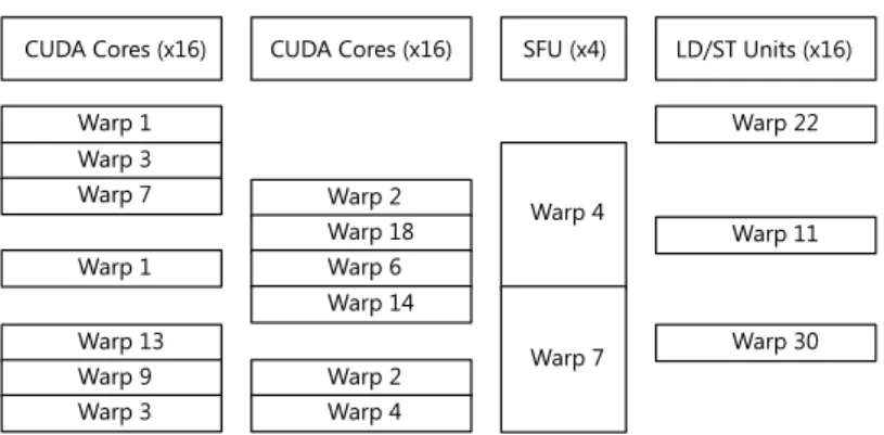
The scheduling algorithm used by the warp schedulers is unknown. It is known, however, that one scheduler manages all warps with odd ids, whereas the other scheduler manages the warps with even ids. Each scheduler can only utilize 16 of the 32 cores — except when scheduling double precision instructions, in which case all 32 cores are used by one of the schedulers and the other scheduler cannot issue any instruction to the cores. Each scheduler can issue an instruction to one of the four execution blocks of an SM; execution blocks are the CUDA cores divided into two blocks with 16 cores each, the group of 16 load-store units, and the four special-function units. Depending on the type of the operation, an issued instruction takes several clock cycle to complete: operations executed on the cores or load-store units take two clock cycles to complete, whereas operations run on the four special-function units take eight cycles to complete. In any case, it takes only one clock cycle to issue the instructions and the warp schedulers can already issue the next instructions to idle units without waiting for previous instructions to complete, as illustrated by figure 2.3.
Figure 2.3: Utilization of Execution Blocks
Giving up individual thread execution in favor of the SIMT model allows the GPU to be designed with less transistors and enables some memory operation optimizations otherwise impossible. A smaller chip usually allows higher clock speeds, and coalescing memory operations performed by many threads into fewer, but larger memory transactions has the potential of significant performance improvements. Moreover, the hardware must fetch and process an instruction only once per warp and not once per thread, allowing these costs to be amortized over many threads [2, 6.1]. However, warps become problematic when threads are allowed to use data-dependent control flow instructions that cause threads to take different execution paths. In graphics programming, shaders used to avoid control flow instructions for performance reasons, and often the decision of which path to take could already be made
at compile-time. With shaders getting more complex and the introduction of general purpose programming, supporting branching efficiently became increasingly important. Compared to older generations of graphics cards, the SIMT architecture employs a sophisticated algo-rithm to support arbitrary branching of individual threads. Basically, divergent control flow is handled by executing all paths serially with all threads not on the current path deactivated. After all paths have completed, all threads execute the same path again in parallel. Thus, the algorithm’s worst case performance reduction is proportional to the warp size. For this reason, CUDA developers try to avoid control flow instructions which cause threads of the same warp to take different paths. In contrast, different warps are executed independently, so there is no performance gain or penalty when they are executing common or disjoint code paths. Since the handling of divergent control flow at the warp level can cause unexpected program behavior, we examine the branching algorithm used by Fermi thoroughly in later chapters and prove its correctness for terminating programs in section 6.
2.2.3 Memories and Caches
Figure 2.4: Fermi’s Memories and Caches
As shown in figure 2.4, there are many different types of memories and caches placed at various locations on the chip. Each one of the 16 streaming multiprocessors has its own register file and shared memory, as well as L1, constant, and texture caches. Threads cannot access the memories and caches of any SM other than the one they are executed on.
A number of registers is assigned to each thread running on a SM, the exact amount depending on the program executed by the threads. Once assigned to a thread, a register is exclusively accessible by its assigned thread and becomes available for reassignment only when the thread terminates. If a CUDA program requires many registers per thread to execute, the maximum number of threads that can be concurrently scheduled on a SM decreases when the SM runs out of register file space. Having less warps available for scheduling might degrade performance, as it becomes more likely that all warps are blocked waiting for the completion of a high-latency operation like uncached DRAM access.
The SM’s shared memory and L1 cache are actually the same on-chip memory that can be configured to provide either 16 KByte of shared memory and a 48 KByte L1 cache or vice versa. Accessing shared memory is almost as fast as accessing a register, so using shared memory is significantly faster than accessing the DRAM. However, Fermi can use the L1 cache to reduce DRAM access times. Furthermore, the 768 KByte L2 cache shared by all SMs also speeds up DRAM accesses, whereas the constant cache is used to speed up access to special constant data in the DRAM. In graphics mode, many pixel shaders sample values from textures stored in DRAM. Although not shown in figure 2.2, all SMs have special hardware units for texture sampling operations that perform address calculations and filtering operations efficiently in hardware. We do not consider texture operations in the following chapters, despite the fact that CUDA programs can indeed use the streaming multiprocessor’s texturing hardware.
The DRAM is shared by all streaming multiprocessors. With up to several gigabytes it is the largest type of memory on the GPU. In graphics mode, the DRAM is used to hold all texture and vertex data. In general purpose computing mode, any data can be stored in the DRAM and all threads have full read and write access.
Based on this hardware-centric overview of the available memory types, section 2.2.3 revisits this topic from the software point of view.
2.2.4 Compute Capability
Since the release of CUDA in 2006, new features have been added to the hardware and subsequently to CUDA as well. The features and instructions supported by a GPU are defined by the GPU’s compute capability, which also specifies some hardware constants like the maximum number of concurrently resident threads on a SM or the number of registers per SM. Fermi’s compute capability is 2.0. The first digit, the major revision number, denotes the core architecture of the GPU. The second digit, the minor revision number, reflects incremental improvements to the core architecture. A device of higher compute capability is backward compatible to a device of lower compute capability, as devices of higher compute capability support a superset of the features of older devices [8, 3, 1.2.1 and 2.5 respectively]. During the writing of this report, Nvidia released the GF104 chip that supports compute capability version 2.1. However, no new instructions were added with version 2.1. The most significant changes concern the architecture of streaming multiprocessors and the fact that the warp schedulers now support the scheduling of two successive, independent instructions of the same warp in parallel [10, 5.2.3 and G.4.1]. The formal semantics defined in the following chapters reflects compute capability version 2.0.
An overview of supported instructions and device parameters for all current GPUs can be found in [3, chapter G.1]. For example, atomic memory operations were introduced with compute capability version 1.1 and are therefore unsupported by hardware of compute capability 1.0. The number of registers per SM has increased from 8192 for devices of compute capability 1.0 and 1.1 to 32768 for Fermi. On the other hand, the warp size remained constant at 32 threads per warp for all currently available GPUs. There are also device parameters, such as the amount of streaming multiprocessors on the chip, that can vary even within the same compute capability version.
As this report focuses solely on Fermi, we consider all CUDA features to be supported by the underlying hardware but still abstract from specific numbers such as the amount of registers per SM, as mentioned above. Since all lower compute capability versions are subsets of compute capability 2.0, it should be possible to construct a formal semantics for
older CUDA versions by removing the unsupported features from the semantic domains and rules defined in the following chapters. However, this report does not explore the feasibility of this idea.
2.3 CUDA Programs
At least for the time being, operating systems such as Windows and Linux launch all pro-grams on the CPU. Therefore, a CUDA application is started on the CPU and must use the CUDA runtime to launch a calculation on the GPU. As the CPU and GPU are usually fully independent chips, they operate in parallel, making explicit synchronization necessary. The graphics driver is responsible for handling the synchronization details and hence hides these complexities from the CUDA developer. The part of the CUDA application that is executed on the CPU is called the host program, whereas the part that is executed on the GPU is called the device program or kernel.
Program 2.1 is a simple CUDA program that squares the values of an array4. It is written in CUDA-C, an extension of the C programming language developed by Nvidia to simplify the development of general purpose applications for the GPU. Even though we use CUDA-C for the introductory example, we eventually switch to using PTX, an assembly level language for GPU programming. We use PTX to define the formal semantics of CUDA, because PTX makes it more explicit what operations are actually performed on the hardware. For example, in CUDA-C we don’t know ifa = 1; is a cached or uncached write, whereas in PTX the statementst.global.ca [a], 1; states the cache operation ca explicitly. By using PTX, we avoid having to “guess” which cache operation to use in this case. PTX is introduced in section 2.3.3.
We explore the basic structure of CUDA programs based on how the host (the CPU) and the device (the GPU) execute program 2.1. When the operation system launches program 2.1, the CPU starts executing the functionmainat line 9.mainis a standard C function which is entirely executed by the CPU. It calls CUDA runtime functions to interface with the GPU, but all interactions with the GPU are completely handled by the CUDA runtime and the graphics driver.
In line 9, two pointer variables are declared that are used to hold the input array which is to be squared by the GPU. In this example, we only start 32 threads on the GPU, therefore we have to allocate enough memory to hold 32 floating point values. The host memory for the array is allocated in line 11 and the pointer to the starting address of the allocated memory is stored ina_h. The next line uses the CUDA functioncudaMallocto allocate an array of equal size on the GPU’s DRAM. The pointer to the address of the array in device memory is stored ina_d; it has no meaning for the host and dereferencing it would very likely result in either an access violation or reading garbage.
The CPU then fills the host array with some values. Afterwards, these values are copied into device memory using CUDA’scudaMemcpyfunction. Botha_handa_dnow hold the same data, once in host memory and once in device memory. This is necessary because the GPU usually has no access to host memory and therefore cannot reada_hdirectly. Now that the GPU has access to all required input data, the CPU launches thesquareArrayfunction on the GPU in line 17. The<<< ...>>>syntax specifies the execution configuration, in this
4Program 2.1 is a simplified version of the program found athttp://llpanorama.wordpress.com/2008/05/
1 __global__ void squareArray (float *a) 2 {
3 int idx = threadIdx .x; 4 a[ idx ] = a[ idx ] * a[ idx ]; 5 }
6
7 int main (void) 8 {
9 float *a_h , * a_d ;
10 int size = 32 * sizeof(float); 11 a_h = (float *)malloc( size ); 12 cudaMalloc((void **) &a_d , size ); 13
14 // Initialize host array ...
15
16 cudaMemcpy(a_d , a_h , size , cudaMemcpyHostToDevice); 17 squareArray <<< 1, 32 >>> ( a_d );
18 cudaMemcpy(a_h , a_d , size , cudaMemcpyDeviceToHost); 19
20 // Use the results ... 21
22 free( a_h ); 23 cudaFree( a_d ); 24 }
Listing 2.1: A simple program written in CUDA-C that squares the values of an array
case it means that the GPU should use 32 threads to execute the function. Also, the pointer to the array in device memory is passed to the GPU.
The GPU runs thesquareArrayfunction defined at line 1, generally called a kernel, once for each of the 32 threads. The Giga Thread scheduler assigns the threads to one streaming multiprocessor. Since the warp size of all current GPUs is 32, the SM puts all threads into one single warp. The warp then executes all 32 threads concurrently. threadIdx.x is a predefined variable accessible by all functions running on the GPU and returns the index of the thread; here a unique value between 0 and 31 is returned for each thread. At line 4, the thread index is used to read the input data from global memory using the pointer passed to the kernel. Subsequently, the squared value is written back to the array. Since thread indices are unique, this means that all 32 elements of the array are squared and updated at the same time.
After the GPU has completed the execution of the kernel, the CPU resumes execution at line 18 where it copies back the result values from device memory into host memory. The CPU can then use the results and eventually frees the memory allocated on both the device and the host before the program exits.
CUDA supports some more complex forms of CPU and GPU synchronization like streams and events described in [3, 3.2.7.5 and 3.2.7.6], whose primary purpose is to improve the level of parallelism between the CPU and the GPU. However, we do not consider any form of CPU/GPU interaction for the remainder of this report and focus solely on the GPU semantics. Now that we have some basic understanding of the structure of CUDA programs, we take a closer look at how CUDA organizes threads on the GPU and the characteristics of the different types of memory available to CUDA programs. Thereafter we give a brief introduction to
the PTX programming language and the compilation process of CUDA programs.
2.3.1 Thread Organization
When a kernel function is launched on the GPU it is executed by many threads in parallel. The hardware automatically assigns a thread index to each thread that the program can use to identify the thread. For example, program 2.1 uses the thread index to read from and write to a specific memory address by using the thread index to access a value of an array. Thread indices are dimensional, because CUDA programs often deal with two- or three-dimensional programs. For instance, a GPU accelerated raytracer might use one thread to calculate the final color of one pixel. The location of a pixel is stored in a two-dimensional vector which can thus be trivially mapped to the thread’s index. While three-dimensional indices are convenient, sometimes a program might also require a thread’s one-dimensional index; the CUDA documentation specifies how a one-dimensional index can be obtained from a three-dimensional one [3, 2.2].
Context n ... Thread (0, 0, 0) Thread (1, 0, 0) Thread (0, 1, 0) Thread (1, 1, 0) Block (0, 0) Thread (0, 0, 0) Thread (1, 0, 0) Thread (0, 1, 0) Thread (1, 1, 0) Block (1, 0) Grid 1 Thread (0, 0, 0) Thread (1, 0, 0) Thread (0, 1, 0) Thread (1, 1, 0) Block (0, 0) Thread (0, 0, 0) Thread (1, 0, 0) Thread (0, 1, 0) Thread (1, 1, 0) Block (1, 0) Grid 2 Context 1
Thread (0, 2, 0) Thread (1, 2, 0) Thread (0, 2, 0) Thread (1, 2, 0)
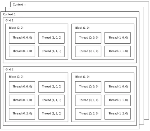
Figure 2.5: CUDA Thread Hierarchy
Figure 2.5 shows how CUDA organizes threads on the GPU. Threads are grouped into thread blocks, also called cooperative thread arrays, and within a thread block each thread index is unique. All threads belonging to the same thread block are executed on the same streaming multiprocessor. When a streaming multiprocessor has free capacity, the Giga Thread scheduler assigns an unscheduled thread block to the SM. The SM creates all threads and allocates the necessary resources to execute them. Threads with consecutive indices are grouped into a warp, i.e. threads 0 to 31 belong to warp 0, threads 32 to 63 belong to
warp 1, and so on. If the amount of threads within a thread block is not a multiple of the warp size, the last warp is not fully populated. Warps are not shown in figure 2.5, because they are not part of the CUDA specification [2, 4.5]. A streaming multiprocessor must have enough resources available to create all threads of a block, otherwise the Giga Thread scheduler cannot issue a pending thread block to the SM. Therefore, the number of thread blocks and threads that can concurrently be allocated on a processor depends on the number of registers each thread requires to execute the program, the number of threads within a thread block, the SM’s register file size, the maximum number of resident warps and blocks allowed on a processor, and the available and required amount of shared memory. Threads of the same thread block can communicate and share data through shared memory and can also synchronize their execution to avoid race conditions when accessing shared memory. Threads not belonging to the same thread block can only cooperate using global memory. However, no synchronization mechanism exists between threads of different blocks, so reading global data written by other threads is generally unsafe.
The streaming multiprocessors assign a unique block index to each block. Blocks are organized two-dimensionally within grids and are distributed among the streaming multi-processors. All blocks of a grid contain the same amount of threads and execute the same program concurrently. When a kernel function is launched, the GPU creates a grid and the required amount of thread blocks and begins distributing thread blocks to available pro-cessing cores. For device of compute capability 2.0, each thread block can consist of up to 1024 threads if not restricted by any other hardware constraints and each grid can contain thousands of blocks. CUDA programs can also access the block index as well as the block and grid dimensions in addition to the thread index, which can be used to uniquely identify a thread within the grid. Referring back to the raytracer example, 1024 threads might not be enough to raytrace an image of acceptable resolution if each thread corresponds to one pixel. Therefore, the calculation must be spread across several thread blocks and processors. If the raytraced image is to be stored in a two-dimensional array in global memory, the memory address where each thread stores its result can be calculated using the thread and block index as well as the block dimension.
Grids belong to a context. A context can consist of many grids with different dimensions that execute distinct programs. Up to 16 grids of the same context can execute concurrently. All grids of the same context share a common virtual address space, thus threads belonging to different contexts cannot access each others memory locations. While there can be several contexts created on the device, only one context can be active at a time. Even though it is not explicitly stated by the CUDA documentation, it is safe to assume that grid execution and therefore also context execution cannot be preempted; Nvidia recently announced that preemption will be a feature supported by future GPUs5.
2.3.2 Memory Types
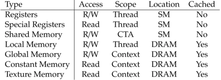
CUDA programs have access to all of the different memory types mentioned in section 2.2.3. We now revisit the topic of memories and caches from the software point of view and look at the restrictions and performance traits of each type of memory.
Figure 2.6 gives an overview of some of the properties of the available CUDA memory types. Registers, special registers, and shared memory are located within the streaming
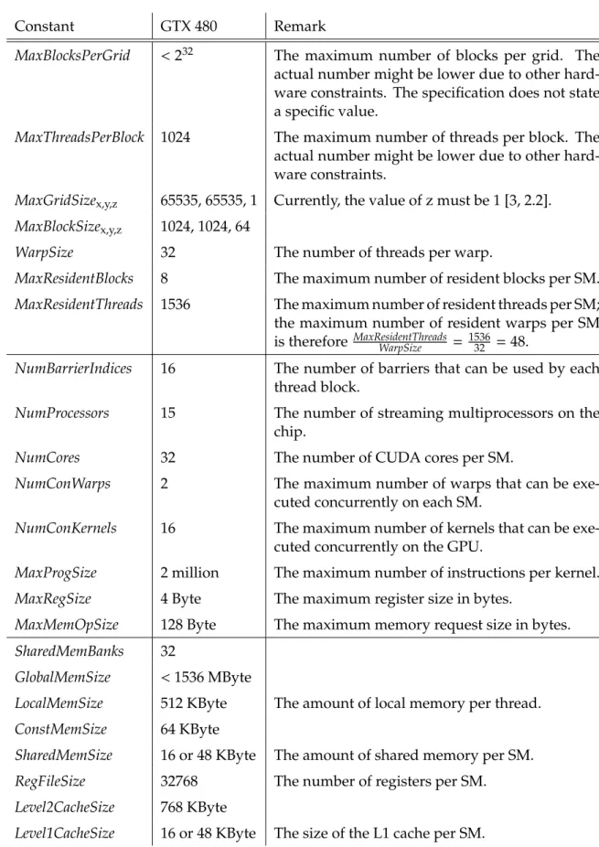
Type Access Scope Location Cached
Registers R/W Thread SM No
Special Registers Read Thread SM No
Shared Memory R/W CTA SM No
Local Memory R/W Thread DRAM Yes
Global Memory R/W Context DRAM Yes
Constant Memory Read Context DRAM Yes
Texture Memory Read Context DRAM Yes
Figure 2.6: Properties of CUDA Memory Types
multiprocessors and are thus only accessible by the SM they belong to. These low-latency memories are not cached, because access times are generally low. On the other hand, the local, global, constant, and texture memories are all distinct sections of DRAM memory located off the chip. Accessing DRAM is at least an order of magnitude slower than accessing on-chip memory, therefore caches are used to amortize the costs.
Whenever threads of the same warp write to the same memory location, the results are unpredictable; the behavior even depends on the compute capabilities of the device the application is executed on. For devices based on the Fermi architecture, only one thread performs the write, but which one is undefined [3, G.4.2]. If more than one thread of the same warp performs an atomic read-modify-write on the same memory location, all operations are serially executed, but the order in which the operations are performed is undefined [3, 4.1].
Registers. When a thread is allocated on a streaming multiprocessor, the SM assigns the required amount of registers to the thread, which are subsequently accessible by this thread only. Each thread belonging to the same grid requires the same amount of registers to execute the program. Register access is fast, but registers might be blocked after being used as an argument for a high-latency operation such as DRAM memory access. For optimal performance, a thread may execute subsequent instructions that do not depend on any of the blocked registers. If a register used by the next instruction is blocked, however, the thread and consequently the thread’s warp cannot be scheduled for execution. In this case, the warp scheduler checks if there is any other warp ready to execute its next instruction and schedules this one instead. That way, latencies can be hidden if only there are enough other warps to execute in the meantime.
Special Registers. Special registers are predefined by the hardware. They convey param-eters like the thread index, the block index, the grid size, and so on to a thread. Obviously, the thread index register returns a different value for each thread of the same thread block, whereas other registers like the grid size register hold the same value for all threads of the same grid. Still, even grid-scoped special registers are duplicated, because threads of the same grid are usually executed on many different streaming multiprocessors, each of which provides its own copy of the register.
Shared Memory. A streaming multiprocessor dynamically partitions its shared memory and assigns one of those partitions to each of its thread blocks. Threads of the same thread block can then share data through their assigned shared memory partition but are unable to access any other partition on the same or another streaming multiprocessor. CUDA does not
attempt to protect the developer from the problems that can occur due to conflicting access to shared memory. Developers must manually take care of race conditions, read-after-write hazards and the like using atomic operations, thread barriers, or memory fences.
Access to shared memory is almost as fast as accessing a register. Therefore, it might be beneficial to copy data located in global memory to shared memory if it is accessed several times by several different threads of the same block.
Shared memory has 32 banks on current GPUs. Banks are interleaved, more precisely, successive 32 bit words are assigned to successive banks. If all threads of a warp access locations in shared memory with locations residing in different banks, all 32 reads or writes can be performed in parallel. However, if threads access locations where two or more locations reside in the same bank, there is a bank conflict and access has to be serialized. For example, if all threads of a warp read data from successive indices of a 64 bit double precision floating point array in shared memory, the reads of threads belonging to the first half-warp are in conflict with the reads of the threads belonging to the second half-warp. Consequently, the reads are serialized and serviced by two independent shared memory accesses. Avoiding bank conflicts has the potential of significant performance improvements.
Local Memory. Local memory resides in DRAM and is slow to access. To improve latency, threads can use the streaming multiprocessors’ L1 caches and the global L2 cache to speed up reads and writes to local memory. A read of a memory address already cached in L1 has a latency that is almost as low as reading a register.
Each thread has its own local memory space and has no access to the local memory of other threads. The local memory is used by the compiler to spill registers to memory when the thread requires more registers than can be reasonably assigned to it. Moreover, the function call stack resides in local memory. Additionally, a thread may use local memory to store other private data that does not fit into registers such as arrays.
With thousands of threads in-flight, the amount of local memory allocated to each thread consumes a significant amount of DRAM. In the case of the GeForce GTX 480, if all streaming multiprocessors were fully utilized and all threads had the maximum amount of local mem-ory allocated, the amount of memmem-ory required would be 11.25 GByte6, which is an order of magnitude more than the available amount of DRAM on the graphics card. The specification does not state what the CUDA runtime does to remedy this situation, so we have to assume that less threads are launched to prevent the program from running out of memory. All in all, the amount of global memory available to a CUDA program is the amount of DRAM memory sans the amount of constant memory and reserved local memory. Consequently, the amount of global memory available to a CUDA program is unknown statically; we only know it is less than the amount of DRAM on the board.
Global Memory. Global memory is shared by all threads of the same context and is not sequentially consistent [9, 5.1.4]. Like for local memory, the streaming multiprocessors’ L1 caches and the global L2 cache speed up accesses to global memory. Conflicting writes to the same address by different threads result in undefined behavior and CUDA does not supply any mechanism for global thread synchronization. The only way to synchronize memory access is thread block synchronization or launching dependent grids within the same stream on the CPU-side. Other than that, atomic operations or memory fences might be helpful in avoiding some of the common shared data issues.
The L1 caches of different streaming multiprocessors are not kept coherent for global memory locations. This can result in a thread reading a stale value from a memory location that has long been updated by another thread [9, table 80]: Suppose thread 1 on SM 1 writes the valueato global memory locationl. On SM 2, thread 2 reads global memory location
lafter the effect of thread 1’s write is visible to all other threads. If a thread on SM 2 has previously accessed locationland the value stored atlis still cached in the L1 cache, thread 2’s read operation returns the stale value from the cache. Then again, this coherency problem only makes an unpredictable situation even more unpredictable, i.e. even without the stale data problem it cannot be statically known whether thread 2 reads the old or the new value at locationl. Thread 2 might read locationlbefore thread 1 even executes the write command, or before thread 1’s write command is fully processed by the memory subsystem. In that case, thread 2 reads the old value. If thread 2 executes the read command after thread 1’s write command is fully processed, thread 2 might get the new value or the old value depending on whether the L1 cache contains a valid cache line for addressl. All in all, reading and writing the same global memory address from different threads should be avoided.
Constant Memory. Constant memory is also located in DRAM and cached by several constant caches [11, IV.J]. Threads can only read constant memory locations; the CPU can also write to constant memory. Before Fermi introduced L1 and L2 caches for local and global memories, access to constant memory was generally faster because of the constant caches that already exited on previous generation devices. Even with cached global and local memory operations, there are still some hardware optimizations that might make reads of constant memory faster than global or local reads.
Constant memory is partitioned into eleven 64 KByte banks on current GPUs. Bank zero is used for all statically sized and allocated constant variables, whereas the other banks are used to support the usage of constant arrays whose size is not known at compile-time. We neglect the concept of constant banks entirely, because allocations of constant memory occur on the host side of a program and are therefore outside the scope of the semantics. At runtime, constant banks introduce no semantically interesting features, as the only complications that arise are some advanced address calculations that are necessary to access different arrays within the same bank. The semantics fully supports any kind of address calculations for all types of addressable memory, so constant banks add nothing new.
Texture Memory. In graphics mode, the GPU typically samples thousands of texels each frame. What makes texture memory special is the layout of the texture data in the DRAM and in the texture caches. Since threads of the same warp typically sample texels that are close together in 2D, the texture memory and caches are optimized for 2D spatial locality [3, 5.3.2.5]. A CUDA application might benefit from this optimization if its data is organized appropriately.
2.3.3 Introduction to PTX
The parallel thread execution virtual machine and instruction set architecture, from now on referred to as PTX, is designed to allow efficient execution of general purpose parallel programs on Nvidia GPUs. PTX provides a stable instruction set spanning several compute capability versions and abstracts from the hardware instruction set of the target device. As already mentioned in section 2.2.4, devices of different major compute capability versions have a different core architectures, whose hardware instruction set might differ. PTX makes
low-level programming possible without tying the program to a specific compute capability version. Section 2.3.4 explains in greater detail how PTX programs are compiled down to the hardware instruction set.
The squareArray kernel of program 2.1 is written in CUDA-C, an extension to ASNI C developed by Nvidia. As the formal semantics developed in this report is close to the hardware, C is already too high-level a language to base the semantics on. We therefore define the formal semantics on an extended subset of PTX. This section focuses on the basic features and characteristics of PTX; more detailed information about PTX can be found in the PTX specification [9].
1 .version 2.1 2 .target sm_20 3
4 .entry squareArray (.param .u32 a) 5 {
6 .reg .u32 arrayIndex ; 7 .reg .u32 address ; 8 .reg .f32 value ; 9
10 ld .param .u32 address , [a ]; 11 mul .u32 arrayIndex , % tid .x , 4;
12 add .u32 address , address , arrayIndex ; 13 ld .global .f32 value , [ address ]; 14 mul .f32 value , value , value ; 15 st .global .f32 [ address ], value ; 16 exit;
17 }
Listing 2.2: PTX version of program 2.1’ssquareArraykernel
Program 2.2 is the PTX version of thesquareArraykernel of program 2.1 already discussed
earlier. The .version and .target directives inform the PTX compiler about the PTX
language version and the target architecture the program is intended to run on. All 1.x PTX programs can be compiled for allsm_2xtargets because of the backward compatibility, the reverse is not possible.
In line 4, the entry pointsquareArrayis defined. Each PTX program can define multiple entry points, so the same PTX program can be used to launch different kernels on the GPU. Like its C counterpart, the kernel has one parameter, a. In the C version, a is a pointer to a floating point array in global memory. In PTX, however, a is an unsigned integer in the parameter state space where the value of the pointer to global memory is stored. Function input and return parameters are stored in registers or in local memory depending on hardware constraints, whether the function is or might be called recursively during the execution of the program, and what is most optimal in terms of performance. It is up to the PTX compiler to decide where the parameters are actually located. In the case of kernel parameters, though, the actual storage location of input parameters is always constant memory [3, B.1.4]. In line 10, theld instruction is used to load the value at addressainto registeraddress. In this case, the compiler replaces the.paramparameter of theldoperation with.const, because the.paramvaluealoaded by this operation lies in constant memory. The address stored in register addressis the location of the floating point array in global memory. In order to access the array at the index corresponding to the thread’s thread index,
the thread index stored in special register%tid.xis first multiplied by 4 in line 11 and then added to the starting address of the array in line 12. This mimics the semantics of the C statementa[idx]: To the location ofa, addidxtimes the size of one element stored in the array. The multiplication with the element size is implicit in C, but explicit in PTX. The size of a floating point value is 4 bytes.
In line 13, the program loads the array’s value stored at the computed address in global memory and squares the loaded value in line 14. The computed value is subsequently written back to the same address in global memory in line 15. The exitstatement in the next line signals the termination of the threads to the warp.
PTX supports five basic types: signed integers, unsigned integers, floating point values, bit (untyped) values, and predicates. Except for predicates, each type can be used with different sizes. For instance,.f32denotes a 32 bit floating point value and.b64specifies a 64 bit untyped value. There are complex conversion rules between the different types, defined in [9, Table 13]. Furthermore, registers are virtual in PTX, so even though we defined two registersarrayIndex andaddressin lines 6 and 7, the compiler might decide to use only one physical register to improve resource utilization on the hardware.
In the following chapters, the formal semantics is defined on an extended subset of PTX. From the features discussed in this section, we ignore data types, the parameter state space, and virtual registers and assume that type checks, parameter state space resolution, and virtual register to physical register mapping have already been performed by a compiler. This allows us to focus on the core semantical issues without being overwhelmed by PTX’ convenience features. The instructions and features supported by the semantics can be found in section 5.1.
2.3.4 Compilation Infrastructure
Nvidia supplies a compiler that separates host and device code of a CUDA-C file and compiles each of those either for the CPU or for the GPU. The device code can either be compiled into PTX or into binary GPU code. Binary code is architecture specific, meaning that code compiled for a device of compute capability x.y can only be run on devices of compute capabilityx.zwithz ≥ y. If a CUDA application has PTX code embedded into its executable file instead, a just-in-time compiler compiles the PTX program into binary code at runtime. This approach has several advantages. First of all, the CUDA application also supports future hardware that was not yet available at compile time, as a PTX program for some specific compute capability can always be compiled for a device of equal or greater compute capability. Moreover, future compiler updates might generate more efficient code, so the application’s performance might increase without the need to recompile and redeploy the application. On the other hand, just-in-time compilation increases application load time [3, 3.1]. Hybrid approaches can be used as well, i.e. code can be compiled ahead-of-time for some devices and just-in-time for others.
Nvidia has recently released a first beta version of cuobjdump disassembler, a tool that decompiles binary code into a PTX-like assembly language. At the time of this writing, cuobjdump disassembler can only be downloaded by registered Nvidia developers, and decompilation of programs compiled for compute capability 2.x targets is not yet supported. Still, some valuable insights can be gained by inspecting the binary code produced by the PTX compiler for 1.x targets. Some of the assumptions that we make in later chapters are based on observations made using the cuobjdump disassembler.
2.4 Alternatives to CUDA
CUDA is a Nvidia exclusive technology, so only Nvidia GPUs are capable of executing CUDA applications. While this exclusivity is beneficial in that the application programming model can be fully optimized for the hardware, it makes it impossible to support other parallel processors such as AMD GPUs or IBM’s Cell chip. Basically, an application supporting both AMD and Nvidia GPUs would have to incorporate two versions of any kernel it executes: One written in CUDA, and one written for the Compute Abstraction Layer (CAL), AMD’s CUDA equivalent [12]7. Both the Khronos Group and Microsoft released cross vendor
parallel computing frameworks to remedy this situation. The remainder of this section briefly compares CUDA to those two competing technologies.
2.4.1 OpenCL
Apple initiated the development of OpenCL. Like the OpenGL graphics API, OpenCL is an open standard developed by the Khronos Group. The specification [13] currently specifies OpenCL version 1.1, which has many similarities to CUDA for devices of compute capability 1.x. Newer CUDA features such as recursion are not yet supported by OpenCL.
CUDA OpenCL
Grid NDRange
Thread Block Work Group
Thread Work Item
Streaming Multiprocessor Compute Unit
CUDA Core Processing Element
Global Memory Global Memory
Constant Memory Constant Memory
Shared Memory Local Memory
Local Memory Private Memory
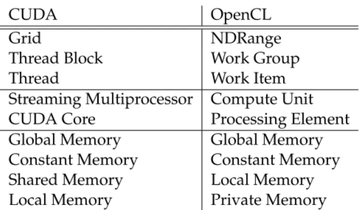
Figure 2.7: Mapping Between CUDA and OpenCL Terminology
Figure 2.7 shows how several CUDA concepts can be mapped directly to their OpenCL counterparts [2, chapter 11]. OpenCL’s thread and memory hierarchies as well as the under-lying hardware model are closely related to CUDA’s ones. This is to be expected, however, as CUDA’s and OpenCL’s main goals are to achieve the highest possible performance. There-fore, the specification must respect the characteristics of the underlying hardware. In contrast to CUDA, the underlying hardware can also be ATI GPUs, x86 CPUs, or IBM’s Cell chip [13, 12].
OpenCL defines a programming language similar to C that is used to develop OpenCL kernels. There is no standalone compiler to create binary code for an OpenCL kernel. The code of some OpenCL kernel is stored within the host program’s executable as a string. Before a kernel can be executed on an OpenCL device, it has to be compiled at runtime. Nvidia’s OpenCL drivers compile a OpenCL program into PTX [14, 2.2.1], but are currently unable to cache the compiled program to emulate CUDA’s precompilation support [15, 10].
7All referenced AMD documents can be found at http://developer.amd.com/gpu/ATIStreamSDK/pages/
In a way, the semantics defined in this report also define a semantics for OpenCL, but we do not check if Nvidia’s compilation process fully preserves OpenCL’s semantics. This is actually unlikely, as OpenCL does not expose the SIMT execution model of Nvidia GPUs [16, 3] which can lead to unexpected program behavior as shown in chapter 6. Current ATI GPUs also organize threads in warps, called wavefronts, so the same problem should also exist for ATI GPUs [17, 1.3.2]. Whereas the warp size is 32 for all current Nvidia GPUs, the wavefront size varies between 16, 32, and 64 for current ATI GPUs [12, Glossary-A-9]. Hence, OpenCL kernels might exhibit vastly different performance characteristics depending on the hardware they are executed on. For a wavefront or warp size ofnthreads, performance is reduced by a factor proportional to n in the worst case. Additionally, OpenCL programs have to deal with different feature sets supported by the hardware.
2.4.2 Direct Compute
Microsoft introduced a new shader type with DirectX 11: compute shaders. Written in HLSL, a high-level C-like programming language for DirectX shaders, compute shaders are similar to CUDA and OpenCL kernels.
CUDA Direct Compute
Grid Dispatch
Thread Block Thread Group
Thread Thread
Streaming Multiprocessor Multiprocessor
CUDA Core Scalar Processor
Shared Memory Group-shared Memory
Figure 2.8: Mapping Between CUDA and Direct Compute Terminology
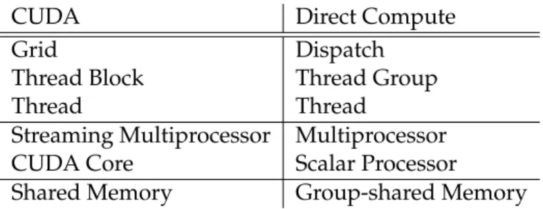
Due to the similarities between CUDA and Direct Compute, it is again possible to map some of the CUDA concepts to their Direct Compute counterparts as shown in figure 2.8 [18]. However, there are some differences concerning memory. In Direct Compute, memory is partitioned into resources, which are either textures or buffers for arbitrary data formats. The application uses resource views for these resources, which define properties like ac-cess patterns or implicit format conversions and subsequently allow the graphics driver to optimize memory access. It is also possible to create several views for the same resource. Compute shaders operate on resource views and can use group-shared memory for thread communication within the same thread group [19].
CUDA, OpenCL and Direct Compute can be used in conjunction with graphics rendering. For computer games, Direct3D is the dominant graphics API and compute shaders can be tightly integrated into a Direct3D 11-based rendering engine. For instance, [20] shows the advantages a deferred rendering implementation using compute shaders has over a tradi-tional pixel shader based implementation; the compute shaders’ greater flexibility makes it possible to render many more lights in the scene at the same performance level. Addition-ally, compute shaders are already used in recent games to accelerate texture compression algorithms8and post processing effects such as screen space ambient occlusion9.
8http://www.pcgameshardware.com/aid,776086, last access 2010-10-10 9http://www.anandtech.com/show/2848/2, last access 2010-10-10
The feature set that must be supported by compute shader compatible hardware is more strictly defined compared to the OpenCL specification. Currently there are two feature levels, one for DirectX 10 compatible graphics cards and one for DirectX 11 compatible GPUs. Once an application has verified that the hardware supports one or both of the feature sets, it can be sure that all of the corresponding compute shader features are supported by the hardware. Still, the specific implementation of a feature might expose different performance characteristics for different hardware devices. Consequently, it might be necessary to develop different implementations of the same algorithm not only because of features unsupported by some hardware, but also because of features running too slow on some hardware.
3 Conventions, Global Constants, and Rules
Due to the low-level nature of PTX and the complexity of CUDA’s programming model, we have to define the domains and rules of the formal semantics in extensive detail. To help reduce the clutter, we introduce some conventions in section 3.1 that at least allow us to express the concepts as concisely as possible. Furthermore, many of the domains and functions defined in chapters 4 and 5 depend on certain parameters like the number of registers per SM or the amount of global memory available on the graphics card. We avoid having to explicitly state the required parameters for each domain and function by declaring these parameters as global constants in section 3.2 and implicitly parameterize all definitions over this set of constants.3.1 Conventions
Throughout the remainder of this report, we use the following conventions in all formal definitions whereever appropriate:
Optional Elements and Failure Elements. We useεand⊥to denote the missing element and the failure element respectively. For some domainA, it is always true that ε < Aand ⊥<A. We define the liftingsAε:=A∪ε,A⊥:=A∪ ⊥, andAε,⊥:=A∪ε∪ ⊥. For somea∈A,
we know thata,εanda,⊥, whereas foraε∈Aε, we only know thataε,⊥, butaεmight be
εor any other element ofA. When we writea∈Aεora= f(a0
) for some function f :A→Aε,
acannot beε, so the selection or assignment is only possible if the selected or returned value is notε. For example, this allows us to shorten some side conditions in function definitions with case distinctions. The following two definitions of function g : A →A⊥ illustrate the usage of this convention. With function fdefined as above, the following two definitions of
gare equivalent: g(a0)= a if a= f(a0) ⊥ if ε= f(a0 ) g(a 0 )= aε if aε= f(a0)∧aε,ε ⊥ if ε= f(a0 )
Functions. Oftentimes, the codomain of some function includes the failure element. Usu-ally the definitions of those functions contain case distinctions. Whenever we do not specify all cases for such a function, the remaining cases are implicitly assumed to return ⊥. Al-ternatively, we use the word “otherwise” to denote a side condition that is true if the side conditions of all other cases are not true. We do not use partial functions.
It is sometimes necessary to change the value a function returns for a specific input. We establish the notation f[a7→b] for some function f : A→Bthat serves this purpose and is defined as follows: f[a7→b](a0)= b if a0= a f(a0) otherwise