STANBUL TECHNICAL UNIVERSITY «««« INSTITUTE OF SCIENCE AND TECHNOLOGY
HIGH ORDER PROGRAMMBLE LOG-DOMAIN FILTER DESIGN
M.Sc. Thesis by Burak DÜNDAR, B.Sc.
Department : Electronics and Communication Engineering Program: Electronics Engineering
STANBUL TECHNICAL UNIVERSITY «««« INSTITUTE OF SCIENCE AND TECHNOLOGY
M.Sc. Thesis by Burak DÜNDAR, B.Sc.
504051204
Supervisor: Prof. Dr. Ali TOKER Members of the Examining Committee: Prof. Dr. Ali ZEK
Assist. Prof. Dr. Serhat K ZO LU
JUNE 2008
HIGH ORDER PROGRAMMBLE LOG-DOMAIN FILTER DESIGN
Date of Submission: 5 May 2008 Date of Defence Examination: 10 June 2008
Tezin Enstitüye Verildi i Tarih : 5 Mayıs 2008 Tezin Savunuldu u Tarih : 10 Haziran 2008
STANBUL TEKN K ÜN VERS TES «««« FEN B L MLER ENST TÜSÜ
YÜKSEK L SANS TEZ Müh. Burak DÜNDAR
504051204
Tez Danı manı: Prof. Dr. Ali TOKER Di er Jüri Üyeleri: Prof. Dr. Ali ZEK
Yard. Doç. Dr. Serhat K ZO LU YÜKSEK DERECEDEN PROGRAMLANAB L R
ACKNOWLEDGEMENT
I would like to thank my supervisor Prof. Dr. Ali Toker for his support and ideas during my M.Sc. thesis.
Also I would like to thank my family for their help and support.
CONTENTS
1. INTRODUCTION 1 2. LOG DOMAIN FILTERING CONCEPT 3
2.1 Log Domain Filtering 3
2.2 Translinear Principle and Translinear Circuits 4
2.3 Synthesis of Translinear Loop Circuits 7
2.4 Biasing Of Translinear Circuits 8
3. LOG DOMAIN FILTER DESIGN TECHNIQUES 12
3.1 State-Space Design Methods 12
3.2 Gm-C Cascading Design Methods 13
3.3 LC Ladder Simulation Design Methods 16
3.4 Comparison of Gm-C and LC Ladder Filters 18 4. HARD DISK DRIVE READ CHANNELS 20 5. DESIGN OF SEVENTH ORDER LOG-DOMAIN FILTERS 23
5.1 Filter Approximations 23
5.2 A Comparison of LC Ladder Prototypes 26
5.3 Design of 7th Order 0.05° Equiripple LC Ladder Prototype 29
5.4 Design of 7th Order Filter Using LC Ladder Simulation Method 30
5.4.1 Log Domain Transconductors 30
5.4.2 Initial Design 32
5.4.3 Modeling Nonideal Effects of Log Domain Filter 39
5.4.4 Improvements on Initial Design 43
5.4.5 Improved Programmability of the New Filter 48 5.5 Design of 7th Order Filter by Gm-C Cascading Method 53
5.6 Comparison of Designed Filters: LC Ladder vs Gm-C 58
5.7 Bias Circuit Design and Programmability 60
TABLE LIST
Page No
Table 2.1 : Comparison of Translinear Loop Types……….. 8
Table 2.2 : A Comparison of Translinear Element Biasing Schemes……… 11
Table 3.1 : A comparison of Log Domain Filter Design Methods…………. 19
Table 5.1 : Common Properties of Designed LC Ladder Prototypes………. 26
Table 5.2 : Calculated Element Values for LC Ladder Prototypes………… 27
Table 5.3 : Exponential Transconductor Cells………... 31
Table 5.4 : The Log Domain Equivalents of Elements in Ideal LC Ladder Prototype ………... 33
Table 5.5 : Theoretical Capacitor Values for 0.05° Equiripple Log Domain Filter………... 35
Table 5.6 : BJT Transistor Parameters Used in Design………. 36
Table 5.7 : Ideal LC Ladder Prototype Vs Initial Design……….. 38
Table 5.8 : The Modifications on Ideal LC Ladder Prototype………... 40
Table 5.9 : Simulation Result Comparison……… 42
Table 5.10 : Comparison of Important Specifications for Improved and Initial Designs……….... 47
Table 5.11 : New Programming Method for the Filter………. 49
Table 5.12 : Programming for Different Bias Currents……… 49
Table 5.13 : Capacitor Values for Gm-C Cascaded Filter……… 56
Table 5.14 : THD values for Different Input Frequencies………... 58
Table 5.15 : THD Values for Different Input Amplitudes………... 58
FIGURE LIST
Page No
Figure 2.1 : Log Domain Filtering Concept……….... 4
Figure 2.2 : Conceptual Translinear Loop……….. 5
Figure 2.3 : BJT as Translinear Element ……… 5
Figure 2.4 : MOS in Subtreshold as Translinear Element ……….. 5
Figure 2.5 : Diode as Translinear Element ………. 6
Figure 2.6 : Example of a Translinear Circuit ……… 7
Figure 2.7 : Identified Translinear Loops……… 7
Figure 2.8 : Diode Connection Biasing………... 9
Figure 2.9 : Emitter Follower Connection Biasing ………. 10
Figure 2.10 : Enz- Punzenberger Biasing……….. 10
Figure 3.1 : Linear Gm-C and Log Domain Gm-C Integrator Concepts……. 14
Figure 3.2 : Conceptual High Order Log Domain Gm-C Filter……….. 15
Figure 3.3 : Passive Filter in Ladder structure……… 17
Figure 3.4 : LC Ladder simulation method Vs Gm-C Cascading (capacitor variations)………... 18
Figure 3.5 : LC Ladder simulation method Vs Gm-C Cascading (transistor mismatch)………... 19
Figure 4.1 : Read Channel Architecture #1………. 21
Figure 4.2 : Read Channel Architecture #2………. 21
Figure 4.3 : Read Channel Architecture #3………. 22
Figure 4.4 : Read Channel Architecture #4………. 22
Figure 5.1 : Butterworth Type Filter Gain and Group Delay Plots…………. 23
Figure 5.2 : Chebyshev Type Filter Gain and Group Delay Plots…………... 24
Figure 5.3 : Bessel Type Filter Gain and Group Delay Plots……….. 25
Figure 5.4 : Equiripple Type Filter Gain and Group Delay Plots……… 26
Figure 5.5 : Schematics of Designed LC Ladder Prototypes………... 27
Figure 5.6 : AC Responses and Group Delays of Designed LC Ladder Prototypes………... 28
Figure 5.7 : 0.05° Equiripple LC Ladder Prototype……… 29
Figure 5.8 : AC characteristics of 0.05° Equiripple LC Ladder Prototype….. 30
Figure 5.9 : Choosing BJT Transistor Size……….. 36
Figure 5.10 : Overall Schematic of 7th Order Log Domain Filter Simulating LC Ladder Prototype……….. 37
Figure 5.11 : Initial AC Simulation Results of the Filter ………. 38
Figure 5.12 : Dissipative Capacitor and Dissipative Inductor……….. 39
Figure 5.13 : Nonideal Effects Added to LC Ladder Prototype……… 41
Figure 5.14 : Effect of Added Nonidealities on LC Ladder Prototype (AC magnitude)……….. 41
Figure 5.15 : Effect of Added Nonidealities on LC Ladder Prototype (group delay)……….. 41
Figure 5.18 : New Proposed Output Stage with EP bias………... 44
Figure 5.19 : Integration of the New Output Stage to the Rest of the Filter …. 45 Figure 5.20 : Comparison of Old and New Designs for the Same Bias Currents……….. 46
Figure 5.21 : THD Comparison for Different Input Amplitudes………... 47
Figure 5.22 : New Programming Concept for the Filter……… 48
Figure 5.23 : Relation Between Current Domains………. 50
Figure 5.24 : Cutoff Frequency Programming……….. 51
Figure 5.25 : Filter Tuning Range………. 51
Figure 5.26 : Group Delay in Tuning Range………. 52
Figure 5.27 : THD in tuning range……… 52
Figure 5.28 : Boost Programming Feature of the Filter ……… 53
Figure 5.29 : The Block Diagram of 7th Order Log Domain Gm-C Filter…... 54
Figure 5.30 : Log Domain Gm-C Structure………... 54
Figure 5.31 : Overall Schematic of 7th Order Log Domain Filter (Gm-C cascading)………... 55
Figure 5.32 : AC Characteristic of Log Domain Gm-C Filter for Different Bias Currents……….. 56
Figure 5.33 : Group Delay of Log Domain Gm-C Filter for Different Bias Currents……….. 57
Figure 5.34 : Tuning Range of the Gm-C Filter……… 57
Figure 5.35 : Sensitivity of LC Ladder and Gm-C Filters to Capacitor Variations………... 60
Figure 5.36 : Bias Circuit……….. 61
YÜKSEK DERECEDEN PROGRAMLANAB L R LOGAR TM K F LTRE TASARIMI
ÖZET
Bu çalı mada hard disk okuma kanalları için iki tane akım modlu logaritmik domende çalı an devre tasarlanmı tır. Öncelikle logaritmik domen filtreleme konsepti ile ilgili temel bilgi verilmi tir. Farklı logaritmik domen filtre tasarlama teknikleri tartı ılmı tır. Sonrasında bir LC basamak türünden devreyi simule eden logaritmik domen filtre tasarımı yapılmı tır. Sözkonusu filtre için dü ük distorsiyonlu bir çıkı katı önerilmi tir. Filtre THD de eri önemli ölçüde iyile tirilmi tir. Ayrıca yükseltme de erinin programlanabilir olmasına olanak veren bir kutuplama stratejisi kullanılmı tır. Sonrasında Gm-C kaskadlama metodu kullanılarak ba ka bir logaritmik domen filtre tasarlanmı ve mevcut tasarım ile kar ıla tırılmı tır. Simülasyonlar AMS 0.35 BiCMOS prosesi kullanılarak yapılmı tır. Tasarlanan filtreler AC genlik ve fazları, lineerlik ve eleman toleranslarına duyarlılılık özellikleri bakımından kar ıla tırılmı tır. Yapılan iyile tirmelerin bu spesifikasyonlar üzerindeki etkileri karakterize edilmi tir.
HIGH ORDER PROGRAMMABLE LOG-DOMAIN FILTER DESIGN
SUMMARY
In this work two different current mode log domain filters for hard disk drive applications are designed. First some theoretical background information is given about log domain filtering concept. Different log domain filter design techniques discussed. Then an LC ladder simulating log domain filter is designed. A new low distortion expanding stage is proposed. THD performance of the overall filter is improved. Also a new biasing strategy that allows boost programming is presented. After that another log domain filter is designed using Gm-C cascading method. Two different filters designed using two different methods are compared. Simulations carried out using AMS 0.35 BiCMOS process. Filters are compared for their AC magnitude and phase performances, linearity, and sensitivity to element values. The effects of the improvements made are also characterized.
1. INTRODUCTION
Log domain signal processing is a valuable method when low voltage, high dynamic range needed from the circuits. Combined with the high frequency operating capability of the current mode operation, these methods become good solutions to overcome the bottlenecks in design. Since signal processing is done in a nonlinear domain, in log domain design the general linearization techniques aren’t needed. Specifications like high dynamic range, low voltage and high frequency are important for the filters used in hard disk drive read channels. So log domain filters are widely used in this type of circuits.
Several design methods have been developed for log domain filter design in literature. Kırcay and Cam (2006) gave some basic information is given on the state-space design methods for log domain filters. Perry and Roberts (1996), Psychalinos and Vlasis (2002), El-Gamal and Roberts (1997), Kontogiannopoulos and Psychalinos (2005) proposed different methods based on LC ladder simulation. El-Gamal and Roberts (2002), Rola and El-Gamal (2003) presented examples for log domain filters designed using Gm-C cascading method.
Sensitivity to element tolerances is a problem in filter design. Since some filter specifications strongly depend on the element values, if the filter sensitivity to element tolerances is high, some unpredicted results may occur. The filters designed using LC ladder simulation methods is claimed to have less sensitivity to element values. On the other hand they have a complicated design methodology compared to Gm-C cascading methods. Also in LC ladder simulating filters, the programmability of the filter specifications (cut off frequency, boost etc…) is not as flexible as in Gm-C cascaded filters. Total harmonic distortion (THD) is generally higher in LGm-C ladder simulating filters than Gm-C cascaded filters.
The main motivation of this work is to combine benefits of log domain filtering and current mode operation with advantage of LC ladder simulation methods. While
log domain filtering concept and translinear principle. In chapter 3 some log domain filter design techniques found in literature are discussed and compared. Chapter 4 presents quick information about hard disk drive read channel architectures and filter specifications used in those architectures. In chapter 5 two filters are designed using two different common methods, they are compared and modified to improve some aspects of the circuits. Chapter 6 is the conclusion of the thesis.
2. LOG DOMAIN FILTERING CONCEPT 2.1 Log Domain Filtering
Log domain signal processing is done by compressing the input signal before processing, processing the compressed signal and expanding it in a similar way to preserve the linearity of the whole system. When the compression is logarithmic and decompression is exponential, the resulting filter is known as a “log-domain filter”. The main advantages of log domain filters can be summarized as;
1. High Dynamic Range.
2. Low Voltage Operation Compatibility. 3. High Frequency Operation.
4. Electronic Tuneability.
Since the log domain filters process the signal after compression, they can operate under lower supply voltage compared to conventional filters. The maximal dynamic range achievable using conventional filter implementation techniques, such as Opamp-MOSFET-C, transconductance-C, and switched-capacitor, becomes severely restricted by the supply voltage. In log domain filters however this dynamic range limitation is relaxed significantly. Also log domain filters have very high frequency capabilities because of their current mode architecture.
Unlike linear filters, in which linear circuits are implemented using nonlinear devices, log-domain techniques directly exploit the nonlinear characteristic of the transistors to linearize the whole filter. So linearization techniques that make the linear filter design process challenging won’t be needed for log domain filters. Without the need for conventional circuit linearization techniques, log-domain filter circuits have a simple and elegant structure, and have the potential to run at high frequencies and operate with low power supplies.
This current signal is then logarithmically compressed using a LOG block. This can be practically achieved by pushing the current into the collector of a bipolar transistor with a grounded emitter terminal. After compression the signal is filtered with proper circuit blocks implemented using translinear principle. The decompression of the signal is performed by an EXP (or ANTILOG) circuit block. Practically, it can be achieved by applying to the base of a bipolar transistor with a grounded emitter terminal. The whole concept is illustrated in Figure 2.1.
Figure 2.1 : Log Domain Filtering Concept
Sometimes it will be necessary to convert the output current to a voltage signal, for example for measurement purposes, using a current-to-voltage converter. [1]
2.2 Translinear Principle and Translinear Circuits
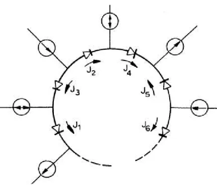
The first idea of "translinear" was suggested by Gilbert in 1975. The word translinear consists of first parts of the words transconductance and linear meaning transconductance linear with current [2]. Bipolar transistor is the main electronic device possessing the translinear principle. It has an exponential relation of current to voltage. The circuit based on the translinear principle is called a translinear circuit. When translinear elements connected together, clockwise or counterclockwise, form a loop that structure is called a translinear loop. A translinear loop concept is shown in Figure 2.2.
Figure 2.2 : Conceptual Translinear Loop
The translinear loop elements are bipolar transistors, MOS transistors operating in subtreshold and junction diodes. These elements can be represented by the graphical representations in the figures 2.3, 2.4 and 2.5.
Figure 2.3 : BJT as Translinear Element
Figure 2.5 : Diode as Translinear Element
A translinear loop can be represented by a translinear circle. A translinear circle is a connected diagram with finite alternating sequence of vertices and directed edges. Each directed edge represents a translinear element. A translinear circle has an equal number of edges in the clockwise (CW) direction and edges in the counterclockwise (CCW) direction.
Tranlinear Principle is expressed as the following: The product of currents directed in clockwise (CW) direction is equal to the products of currents directed in opposite direction(CCW).
In a translinear loop sum of voltage drops on the translinear elements is zero.
(2.1)
After a set of analytical manipulations equation leads to
(2.2)
where In is the current flowing through a translinear element.
Translinear loops can be identified in circuits using a systematic way proposed in [3]. In a circuit containing translinear elements, to identify the translinear loop a dead graph of the circuit is obtained. To obtain a dead graph from the circuit;
1. Independent voltage sources are replaced by short circuits. 2. Independent current sources are replaced by open circuits.
In the dead graph any circle (closed loop) identifies a translinear loop. And for every translinear loop the equation above holds. For example the circuit in Figure 2.6 contains bipolar transistors which can be considered as a translinear element. From the dead graph given in Figure 2.7, translinear loops are easily identified.
Figure 2.6 : Example of a Translinear Circuit
For this example the transistors Q1-Q2-Q3-Q4 and transistors Q4-Q5-Q6-Q7 form translinear loops.
Figure 2.7 : Identified Translinear Loops 2.3 Synthesis of Translinear Loop Circuits
Synthesis of translinear circuits is a straightforward procedure. Translinear-loop circuits can be synthesized as follows.
1. Obtain the translinear loop equations. These can be the functions to implement.
2. Build a translinear loop for each of the equations. 3. Bias the translinear loops.
4. If possible simplify the overall circuit buy merging loops.
The class of translinear circuits is capable of realizing a wide range of linear and nonlinear relationships. However, not all functions are directly implementable by translinear circuits; we can directly realize products, quotients, power-law relationships, polynomials, rational functions, and various combinations of such relationships.
Once a set of translinear-loop equations is obtained, designer must construct a closed loop of translinear elements for each one. In general, there will be more than one translinear loop that implements any given translinear-loop equation. The choices of loop topology and current ordering must be guided by experience and other system-level design considerations. When synthesizing translinear circuits, stacked or alternating loop topologies can be used [4]. The main properties of these topologies are summarized in the Table 2.1.
Table 2.1 : Comparison of Translinear Loop Types Alternating Loop
Topology Stacked Loop Topology Power Supply
Requirement Low High
Biasing Multiple matched bias
sources are required Same bias current can be used through multiple translinear elements Input Current Multiple copies may be
needed. Single copy of input current is enough
2.4 Biasing Of Translinear Circuits
Biasing of a translinear loop is important to maintain the operation of a translinear circuit. Generally translinear loops are biased by forcing a current into the emitter or collector of each input translinear element in the loop and arranging some type of
local negative feedback around it. This feedback adjusts translinear element’s gate-emitter voltage.
There are three main biasing schemes for translinear elements. These are; 1. Diode Connection Biasing.
2. Emitter Follower Connection Biasing. 3. Enz-Punzenberger Biasing.
Figure 2.8 below shows the common diode connection biasing. A current is forced into the collector of the translinear element. This increases its collector voltage. This increased voltage is fed back to the base of the translinear element by diode connection. If any mismatch occurs between the collector current and the input gate voltage of the translinear element adjusted in order to reduce the mismatch. If the collector current is bigger than the input current, the gate will discharge, reducing the gate-to-emitter voltage.
Figure 2.8 : Diode Connection Biasing
Figure 2.9 shows an emitter-follower connection. In this type of biasing a current is sinked from the emitter of the translinear element. In this configuration the emitter voltage will adjust itself up or down so that the emitter current balances the input current. If the emitter current is larger than the input current, the emitter voltage will charge up, reducing the gate-to-emitter voltage. This will reduce the emitter current of the translinear element, this will continue until the currents are matched. If the input current is larger than the emitter current, the emitter will be discharged, increasing the gate-to-emitter voltage, thereby increasing the emitter current until the currents balance.
Figure 2.9 : Emitter Follower Connection Biasing
Figure 2.10 shows a simple alternative to the emitter-follower connection for biasing clockwise translinear elements. This biasing scheme is also called Enz-Punzenberger since it’s first proposed by Enz and Punzenberger. Again here a current is forced into the collector of the translinear element. The collector voltage is sensed by another transistor to adjust the emitter current of the translinear element. This feedback element could be a MOS or bipolar transistor. When a large input current is inserted the collector voltage of the translinear element will increase. Since the collector voltage is tied to the gate (or base) of the feedback transistor, its current will also increase. Pulling more current from the translinear element will increase the emitter current of it. So the currents will tend to equalize. A similar mechanism occurs for small input currents.
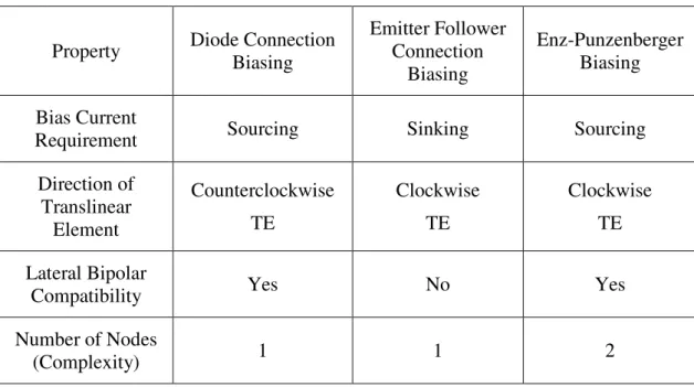
Table 2.2 is comparing the important properties of biasing schemes discussed above. Table 2.2 : A Comparison of Translinear Element Biasing Schemes
Property Diode Connection Biasing Emitter Follower Connection Biasing
Enz-Punzenberger Biasing Bias Current
Requirement Sourcing Sinking Sourcing
Direction of Translinear Element Counterclockwise TE Clockwise TE Clockwise TE Lateral Bipolar
Compatibility Yes No Yes
Number of Nodes
3. LOG DOMAIN FILTER DESIGN TECHNIQUES
In literature there are 3 main design methods for log domain filter design. All other methods consist of improvements and additions to these methods. These two main methods are;
1. State-Space (SS) Design methods 2. Gm-C Cascading Design Methods 3. LC Ladder Simulation Design Methods
These three methods have advantages or disadvantages over each other. Now these three techniques will be discussed briefly.
3.1 State-Space Design Methods
There is a set of first-order differential equations in a state-space formulation. The state variables are equal to simple functions of exponentials of node voltages. There is a one-to-one correspondence between the mathematical formulation and the circuit realization. So a systematic circuit implementation can be developed.
The state space synthesis method for log domain filters can be summarized as follows;
1. Find a suitable state-space description for the filter.
2. Write an exponential mapping function to the input and state variables. 3. Manipulate the equations to obtain a set of nodal equations.
4. Design the circuit elements like transistors, grounded capacitors, and current sources.
The first step used to synthesize a mapped state-space filter is to obtain appropriate system equations [5]. u b x A x t = + ∂ ∂ (3.1)
du
x
p
y
=
T+
(3.2)Here u, y and x denote global input, output, and state vector respectively.
The second step is the mapping. A mapping must be applied to the input and each state,
)
(
v
of
u
=
(3.3))
(
i if
v
x
=
(3.4) where i= 1,2,…,N.Substitute these functions into of Eq. 3.1 and Eq. 3.2, and divide scale each line with
)
(
i i iv
f
v
c
∂
∂
(3.5)where the Ci ’s are arbitrary constants. We obtain the following equation 3.6:
(3.6)
These equations are a set of nodal equations. In fact, if we let vi symbolize the I-th
node voltage in a circuit, then the left-hand side of Eq. 3.6 represents the current flowing into a grounded capacitor. In the same manner, the right-hand side of Eq. 3.6 is the sum of some currents flowing into this capacitor. These currents are a form of voltage-controlled current sources, or transconductance. [5]
3.2 Gm-C Cascading Design Methods
In Gm-C continuous time filters, the transconductor often has to be linearized in order to achieve the desired dynamic range. Log-domain circuits exploit the
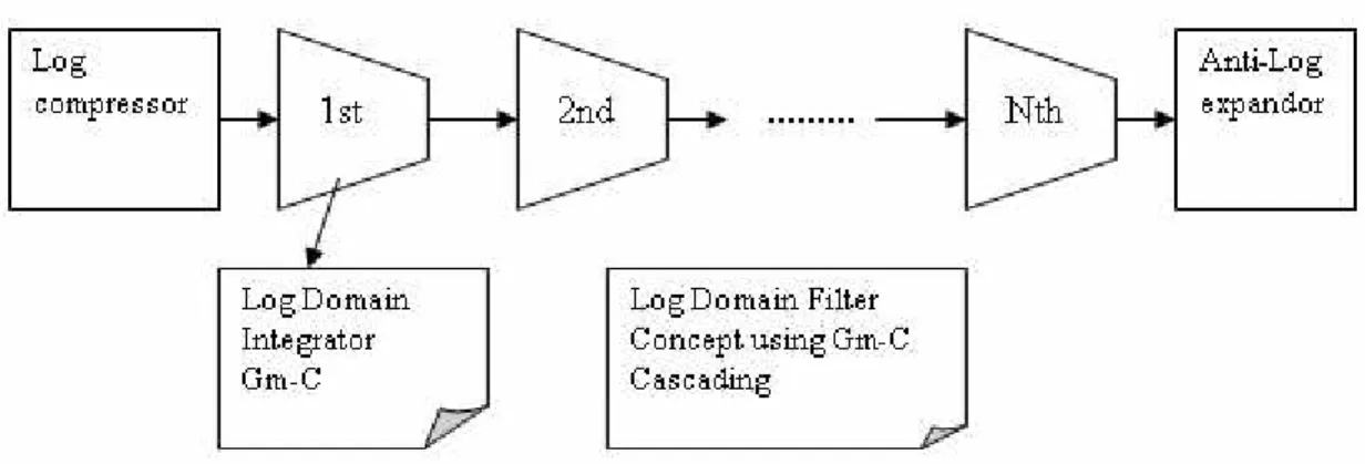
The log domain integrators are the basic building blocks for Gm-C cascaded log domain filters.
Figure 3.1 : Linear Gm-C and Log Domain Gm-C Integrator Concepts The linear Gm-C integrator shown in the Figure 3.1 realizes the following equation;
t
V
c
V
g
out in m∂
∂
⋅
=
⋅
(3.7)The log domain Gm-C integrator realizes;
t
e
U
c
e
U
g
T out T in U V T U V T m∂
⋅
∂
=
⋅
⋅
∗ ∗/(
/)
(3.8) Rearranging the equationt
V
c
e
I
V V V U out S T out sh in∂
∂
⋅
=
⋅
( ∗+ ∗− ∗ )/ ∗ (3.9) The log domain Gm-C integrator facilitates the same integration function. But instead of realizing this function with actual signals, it processes the compressed voltage signals.In order to map a linear domain integrator to a log domain integrator the following transformation equations;
)
/
ln(
T TV
U
U
V
∗=
⋅
(3.10) orT U V T
e
U
V
=
⋅
*/ (3.11)can be used. Here UT = kT/q is the thermal voltage.
As it can be realized from the equations 3.10 and 3.11, the voltages within the log-filter are in the log-domain, while the currents are still in the linear domain.
The integration time constant of the log domain integrator can be derived [6]
m f T U V S T
g
c
c
I
U
c
e
I
U
⋅
sh T⋅
=
⋅
=
=
(
/
)
− */(
/
)
τ
(3.12) where ) / (Vsh UT S fI
e
I
=
⋅
∗ (3.13)The time constant is determined by C and gm = I f / UT corresponding to a
small-signal transconductance. Log-domain filters therefore use the maximum gm/I while
having a dynamic range much larger than the corresponding small signal circuit. In addition, a large gm tuning range is obtained thanks to the validity of the exponential
characteristic of bipolar transistors over several decades.
Figure 3.2 : Conceptual High Order Log Domain Gm-C Filter
As in linear domain synthesis of the Gm-C filters can be done by cascading integrators properly. Figure 3.2 shows the conceptual filter obtained by Gm-C cascading. Blocks for Log and Anti-Log conversion must be placed at the input and output of the filter.
3.3 LC Ladder Simulation Design Methods
Log domain filter design based on LC ladders is preferred for its tolerances on component drifts and parasitic effects. The filters designed with LC ladder simulation methods carry the characteristics advantages of LC ladders, they simulate. In addition to that advantages of log domain operation is also preserved.
In literature there are many works done on LC Ladders simulating filters and their design methodologies. For example in the case of elliptic filters. Some improvement techniques have been discussed literature. In [6] elliptic low pass filter was realized using a floating capacitor to approximately perform the required differentiations. In [7] an alternative SFG representation of elliptic LOG-domain filters is introduced. In this method the SFG of the LC ladder prototype is modified in such a way, that differentiation operation is not required. This is achieved through a manipulation of the voltage/current equations of the LC ladder, so that only lossless integrators and amplifiers are needed. Also improvements on LC simulation method have been reported for band pass filters. [8]
The main and generic procedure in design of a Log Domain filter based on LC ladders can be summarized as the following;
1. Choose an approximation method for the filter
2. Design the LC ladder prototype realizing the chosen approximation method and required specifications.
3. Optionally a Signal Flow Graph (SFG) of the prototype circuit can be extracted. (In some design methodologies this step could be unnecessary) 4. Obtain the log domain equivalents of the necessary elements such as inductor
or capacitor and their different combinations.
5. Replace the LC ladder prototype elements with the obtained log domain equivalents.
The procedure above is a generic design process. So the methodologies developed in literature mainly follow the same procedure. They have slight differences at obtaining the log domain equivalents. Some of them use exponential transconductor cells [9], some of them use Bernoulli cells [10]. But all of these basic cells are designed using translinear principle. According method proposed in [9], the elements of the passive prototype filter is replaced its log domain equivalent in log
domain. The current that flows through the terminals of the passive element in the linear domain is the same with that flows through the terminals of the corresponding active block in the log domain. In this way, the linear operation of the whole filter is preserved. The voltages of the log domain filter are compressed to provide log domain filtering advantages.
Figure 3.3 : Passive Filter in Ladder structure
Consider the current-mode LC ladder filter shown in Figure 3.3. When the passive elements in prototype are replaced by an appropriate active block, the current-voltage relationship of the passive element is implemented. But this replacement procedure should provide the following conditions;
1.The current that flows into the terminals of passive element would be equal to that flows into the corresponding terminals of its active equivalent,
2. The voltage at each terminal of passive element would be equal to the voltage at the corresponding terminal of its equivalent.
If log domain filtering is to be applied, the active blocks will be nonlinear and, thus, the above conditions must be changed as:
1. The current that flows into the terminals of passive element in the linear domain would be equal to that flows into the corresponding terminals of its active equivalent in the log domain,
2. The voltage at each terminal of passive element in the linear domain would be equal to the expanded voltage at the corresponding terminal of its equivalent in the log domain.
3.4 Comparison of Gm-C and LC Ladder Filters
In this section a comparison of Gm-C cascaded and LC ladder simulating filters will be given based on [11].
The state space design method is a straight forward and mathematical method for designing log domain filters. But when the order of the filter is increased, the equations could become too complex to manipulate and solve. As a result for high order filter designs state space method is not preferable.
The Gm-C cascading method is an easy and quick way to design log domain filters. The high order filters can be designed by simply cascading the integrators. Also the tuning can be done easily. Different parameters such as gain, cutoff frequency or boost can be tuned independently. But the problem with Gm-C cascading design methods is the sensitivity of the circuit parameters to the element tolerances. So the circuit parameter drift due to the element tolerances can be a problem. The same problem exists not only in log domain but also in linear domain filters. By making the key aspects of the filters tunable these problems can be relaxed.
The LC ladder simulation design methods carry an important advantage arising from the LC ladder prototypes. LC ladder prototypes have very low sensitivities to element tolerances. So the active log domain filters simulating these LC ladder prototypes carry the same advantageous properties. This fact is illustrated in Figure 3.4 and Figure 3.5. LC ladder structures demonstrate a better sensitivity to transistor area mismatches than the cascade structures. This fact has been remarked in [11].
Figure 3.4 : LC Ladder simulation method Vs Gm-C Cascading (capacitor
Figure 3.5 : LC Ladder simulation method Vs Gm-C Cascading (transistor mismatch)
The difficulty in design process varies for different methods. Some of them use quick and easy procedures for simulating LC ladders.
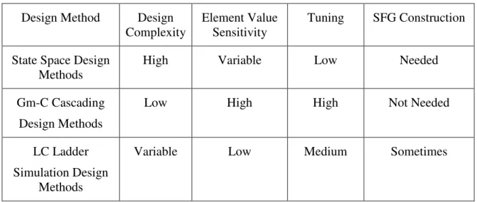
Table 3.1 compares some of the critical properties of design methods; Table 3.1 : A comparison of Log Domain Filter Design Methods
Design Method Design
Complexity Element Value Sensitivity Tuning SFG Construction State Space Design
Methods High Variable Low Needed
Gm-C Cascading Design Methods
Low High High Not Needed
LC Ladder Simulation Design
Methods
4. HARD DISK DRIVE READ CHANNELS
The recording density of the hard disk drive (HDD) systems is increasing rapidly. But the sizes of the bit cells are becoming smaller and smaller. That fact results in hard constraints on the magnetic head: the size, positioning, and sensing of the head media require tighter control on precision and on tolerance. Noise and distortion also corrupt the analog signal obtained from the magnetic head. ISI (inter symbol interference) is the main source of distortion in HDD systems. Also some contribution is introduced from the electronics and the head media. The amplitude of the signal at the output of the head is typically in the microvolt range. So it needs preamplifying circuits to properly recover and use the detected signal. This task is performed by a low-noise amplifier followed by a variable gain amplifier (VGA). To avoid adding distortion to the phase response of the read signal from the amplifying circuits, the cutoff frequencies of the preamplifier and of the VGA are typically a factor of two higher than that of the following low-pass filter (LPF). [12]
In a HDD read channel AFE (Analog Front End), the LPF serves three main functions [13];
1. LPF limits the noise band on the read channel.
2. LPF helps equalize the signal delay within desired targets.
3. LPF enhances the pulses coming on the read channel (by pulse-slimming) and reduces the overlap of the pulses known as Inter-Symbol Interference (ISI). In order to maintain these functions, LPFs, employed in the AFE of a HDD read channel, are generally high order Bessel or 0.05° phase equiripple type filters. These filters are also equipped with a programmable gain boost around cutoff frequency, and possibly a varying cutoff frequency to enable processing of different signals apart from the read channel signal.
The signal from the read head of the HDD comes with a distorted group delay. So it has to be equalized without losing any information from the content. For this reason Bessel and 0.05° phase equiripple type filters are prime implementations of the LPF
due to their excellent group delay characteristics. And also some signal conditioning and pulse shaping may be required to avoid overlap. For this reason LPF must be with the programmable boost feature around cutoff frequency. Since the spectral content of sharp pulses is mainly composed of high frequency components, a gain close to the filter cutoff would boost such components and suppress lower frequency components. The result is a slimmer pulse and a lesser likelihood of ISI. On the other hand this specifications and functions can change based on the chosen read channel architecture. Figure below shows the read channel architectures used in HDD applications. Specification and design complexity of LPF is relaxed or hardened according to HDD read channel architecture.
Figure 4.1 : Read Channel Architecture #1
Architecture #1 in Figure 4.1 was firstly developed by IBM. CMOS and BiCMOS implementations of this architecture can be found in literature. This architecture requires a full 6bit ADC and a digital FIR equalizer.
Architecture #2 in Figure 4.2 is an extension of #1. Only difference is in #2 timing recovery is performed in digital domain. Of course this can relax the specifications on LPF.
Figure 4.3 : Read Channel Architecture #3
Architecture #3 in Figure 4.3 trades the complexity of a continuous time filter to a simpler LPF and a FIR equalizer. The specifications on the filter are further relaxed.
Figure 4.4 : Read Channel Architecture #4
Both architecture #3 and #4 (Figure 4.4) places equalization before ADC so that quantization noise enhancement is eliminated and less number of levels in quantizer is needed. [14]
5. DESIGN OF SEVENTH ORDER LOG-DOMAIN FILTERS 5.1 Filter Approximations
Gain and phase characteristic of a filter can be realized by using more than one transfer function. Time domain, frequency domain responses and the application determines the transfer function to be used. Sometimes there might be trade offs for performance against design complexity. Some important approximation methods for filter design are; Butterworth Filter, Butterworth Filter , Bessel Filter, Linear Phase Filter with Equiripple Phase Error.
The Butterworth filter gives a good attenuation and a good phase. There is no ripple in the pass band or the stop band; because of this, it is sometimes called a maximally flat filter. But the transition from stop band to passband is not very steep. It has average transient characteristics in the passband. Figure 5.1 shows the gain and group delay plots for Butterworth type filters.
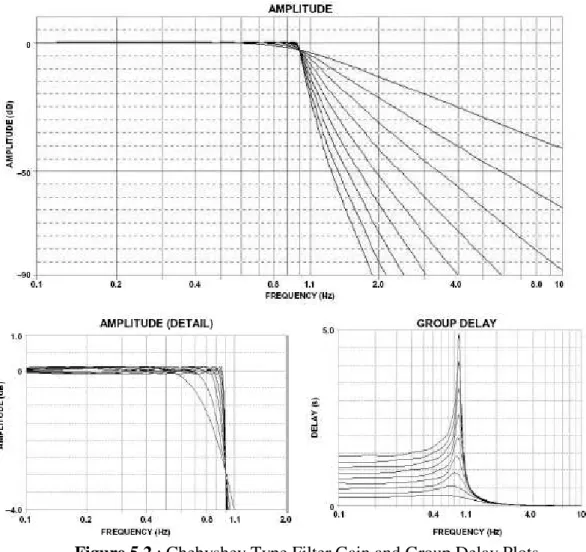
The Chebyshev filter’s transition region is steeper than the same-order Butterworth filter, at the expense of ripples in its pass band. Chebyshev filter minimizes the height of the maximum ripple. The order of the filter also determines the characteristic in passband. For odd order Chebyshev filters begin with 0dB gain and go to ripple value. Even order filters begin from passband ripple value. The number of cycles of ripple in the passband is equal to the order of the filter. Figure 5.2 shows the gain and group delay plots for Chebyshev type filters.
Figure 5.2 : Chebyshev Type Filter Gain and Group Delay Plots
The Bessel filter is optimized to obtain better transient response due to a linear phase in the pass band. This means that there will be relatively poor frequency response. Figure 5.3 shows the gain and group delay plots for Bessel type filters.
Figure 5.3 : Bessel Type Filter Gain and Group Delay Plots
The linear phase filter has a linear group delay characteristic in the passband. Compared with Bessel filter this linearity could extend far beyond the cutoff frequency of the filter. But this linearity is obtained by letting the phase response have ripples, similar to the amplitude ripples of the Chebyshev. The more ripple, the group delay of the filter has, the more linearity extends. The step response will show slightly more overshoot than the Bessel and the impulse response will show a bit more ringing. These filters are also called equiripple phase filters. Figure 5.4 shows the gain and group delay plots for linear phase type filters.
Figure 5.4 : Equiripple Type Filter Gain and Group Delay Plots 5.2 A Comparison of LC Ladder Prototypes
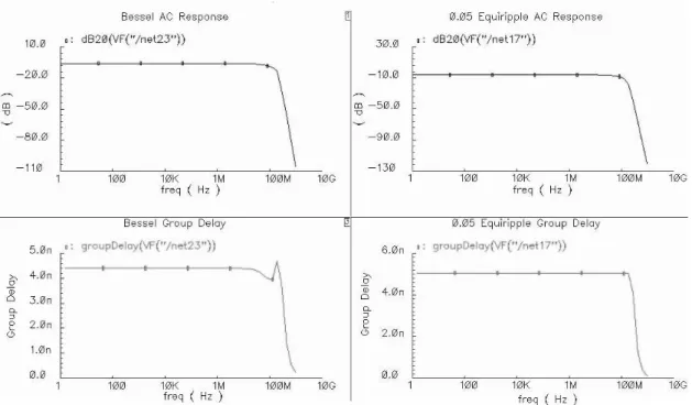
In section 5.1 some properties of filter approximations are given. For hard disk drive read channel filter two candidates exist; Bessel filter and 0.05 Equiripple type. Using Cadence Spectre simulator examples of these two filter prototypes have been designed. And properties of the filters are observed and verified.
Both filter prototypes are designed with the following common properties (Table 5.1):
Table 5.1 : Common Properties of Designed LC Ladder Prototypes 3dB Cut Off Frequency 100MHz
Order of the filter 7th Input Impedance (Zin) 1 ohm Output Impedance (Zout) 1 ohm
The calculated ideal element values for the LC ladder prototypes are shown in Table 5.2.
Table 5.2 : Calculated Element Values for LC Ladder Prototypes
Element Name Bessel Type LC Prototype Element Values 0.05 Equiripple LC Prototype Element Values C1 176.02537 pF 331.838 pF L2 518.6859 pH 795.155 pH C3 835.4 pF 1.059 nF L4 1.117 nH 1.197 nH C5 1.383 nF 1.392 nF L6 1.1759 nH 1.696 nH C7 3.606nF 3.636 nF
Using these element values the schematics of the prototypes (Figure 5.5) are formed and they are simulated using Cadence Analog Design Environment.
Figure 5.6 shows the plots of AC magnitude and phase for ideal prototypes.
Figure 5.6 : AC Responses and Group Delays of Designed LC Ladder Prototypes As expected the phase characteristics of these filters are suitable for HDD read channels. They both exhibit excellent phase characteristics in the passband. Since the in Bessel type filter the group delay flatness is limited to cutoff frequency, but in 0.05° Equiripple filter this flatness exceeds cutoff frequency. Since the degree of the filter is selected small enough, the ripples in phase characteristics are negligible. So the 0.05° Equiripple prototype is selected for the seven order log domain filter.
5.3 Design of 7th Order 0.05° Equiripple LC Ladder Prototype
Since 0.05° equiripple type LC ladders have better group delay performance than the Bessel types, the choice is equiripple. The designed LC ladder prototype specifications and element values are given below. The choice of RL and RS values
will be dependent on the bias current value of the actual filter. The initial value of actual filter’s bias current is chosen Io = 100µA.
(5.1)
So the calculated value for source and load resistance of the prototype filter is
Ω = = 250 100 25 A mV R µ
The LC ladder prototype is shown in Figure 5.7.
Figure 5.7 : 0.05°Equiripple LC Ladder Prototype
The designed cut off frequency is 100MHz. As expected group delay flatness extends to 200MHz range ( 2fC)
Figure 5.8 shows the AC simulation results for 0.05° equiripple ideal LC ladder prototype.
Figure 5.8 : AC characteristics of 0.05° Equiripple LC Ladder Prototype 5.4 Design of 7th Order Filter Using LC Ladder Simulation Method 5.4.1 Log Domain Transconductors
In LC ladder simulation methods the elements of LC ladder prototypes are simulated using log domain equivalents of ideal elements in log domain. These log domain equivalents generally obtained using transconductors. When log domain operation is required, transconductors become log domain transconductors. In literature many transconductor topologies are proposed. All of them use translinear principle and the exponential characteristics of the bipolar transistors. In [9] a set of different transconductor cells are proposed. These transconductors are named positive or negative exponential transconductor cells. Negative exponential transconductor cells realize the same function as the positive ones. But the only difference is negative cells sink the output current, while positive ones are sourcing. This fact brings a minus sign in front of the defining equations of the positive cells.
Table 5.3 : Exponential Transconductor Cells [9] Exponential
Transconductor Cell Type
Transistor Level Schematic Equation
Single-input negative exponential transconductor
cell (E- cell).
T V in V O OUT
I
e
I
=
⋅
ˆ / Single-input positive exponential transconductorcell (E+ cell).
T V in V O OUT
I
e
I
=
−
⋅
ˆ / Dual-input negative exponential transconductorcell (E+ cell).
I
OUTI
Oe
Vin Vout VT/ ) ˆ ˆ ( −
⋅
=
Dual-input positive exponential transconductorcell (E- cell).
T V out V in V O OUT
I
e
I
=
−
⋅
(ˆ −ˆ )/5.4.2 Initial Design
After designing and verifying the LC ladder prototype, an initial form of actual log domain filter is designed. The elements in LC ladder prototype are simulated in log domain. In order to do that the ideal elements are replaced with log domain equivalents. These equivalents designed using the exponential transconductor cells mentioned before. The LC ladder prototype has 3 different types of elements which are; Grounded Resistor, Floating Inductor and Grounded Capacitor.
So for the actual filter design, the equivalents of these elements will be needed. These elements are chosen from the proposed topologies in [9]. In order to understand the operation of these proposed topologies two functions called EXP and LOG are defined.
T V V T
e
V
V
V
EXP
V
=
(
ˆ
)
=
⋅
ˆ/ T−
(5.2))
ln(
)
(
ˆ
T T TV
V
V
V
V
LOG
V
=
=
⋅
+
(5.3)These functions are used to convert elements from log domain to linear domain and from linear domain to log domain respectively. While doing this conversion in order to preserve the linearity of the whole topology the currents of the elements replaced must be equal to the ideal prototype element currents.
The summary of the proposed topologies and their design equations are shown in Table 5.4. As seen from the table the resistor value is determined by the value of the bias current. The capacitor value in grounded capacitor equivalent circuit is same as the ideal LC ladder capacitor value. The capacitor value in floating inductor equivalent circuit is determined by both the inductor value of the ideal LC ladder and the bias current.
Table 5.4 : The Log Domain Equivalents of Elements in Ideal LC Ladder Prototype LC
Ladder Prototype
Element
Element Schematic Design
Equation for Log Domain Grounded Resistor (R) O T I V Rˆ = Floating Inductor (L) 2 2 ˆ T O V I L C = ⋅ Grounded Capacitor (C) C Cˆ =
In order to analyze the topologies mentioned above, the equations of elements in linear domain are a good start. The linear domain equation for a grounded resistor is
R V
I = (5.4)
applying equation (5.2) to (5.4), equation (5.5) is obtained.
R V e V I T V V T T − ⋅ = / ˆ (5.5) To preserve linearity of an element and to simulate it in log domain the currents in log domain and linear domain must be equal. Assuming the resistor equivalent in log domain will be realizing equation (5.6),
O V V O
e
I
I
I
ˆ
=
⋅
ˆ/ T−
(5.6) O T T V V T I V V e V I I T − ⋅ = = / ˆ ˆ (5.7) Equation (5.6) can be rewritten as (5.7) which can be realized using single input exponential transconductor cell as shown in Table 5.4. Next element needed to simulate in log domain is the floating inductor. The linear domain equation of a floating inductor is as in (5.8).−
= 1 (V1 V2)
L
I (5.8)
Again applying EXP function defined in (5.2), equation (5.9) is obtained. ) ) ˆ ( ) ˆ ( ( 1 2 1 − = EXP V EXP V L I (5.9)
The dual input exponential transconductor cells in the log domain inductor topology perform the subtraction and the integration. The resulting current flowing through log domain equivalent is given in (5.10).
) ) ˆ ( ) ˆ ( ( ˆ ˆ 2 1 2 2 − ⋅ = = EXP V EXP V V C I I I T O (5.10)
The capacitor equivalent the current and the voltage of the circuit are equal to the current and the voltage the ideal LC ladder element. This may be obtained from the KCL at node A (Table 5.4) and using the equations of transconductor elements.
T A C T V V V O V A V V O
e
I
e
I
⋅
(ˆ−ˆ )/=
⋅
(ˆ −ˆ )/ (5.11)V
V
ˆ
C=
ˆ
(5.12)The current flowing through the equivalent circuit is given in (5.13).
O V V O
e
I
I
I
I
=
ˆ
=
⋅
A/ T−
(5.13)The theoretical element values are calculated using the equations in Table 5.4. These results are summarized and compared with ideal LC ladder prototype element values in Table 5.5.
Table 5.5 : Theoretical Capacitor Values for 0.05° Equiripple Log Domain Filter Element value
@LC ladder prototype
Element value @Log domain filter
Name of the passive element @LC ladder prototype 1.32735 pF 1.32735 pF C0 198.9 nH 3.1824 pF L1 4.235 pF 4.235 pF C1 299.251 nH 4.788 pF L2 5.55697 pF 5.55697 pF C2 424.586 nH 6.7933 pF L3 14.5435 pF 14.5435 pF C3
The whole design is made for AMS 0.35µ BiCMOS process. This process has a peak fT of 30GHz at 80µA/µm. Process also have vertical pnp transistors. For log domain
equivalents of the passive elements we used “npn121” transistor of the process which has 1 emitter, 1 collector and 2 bases. The emitter area of the transistor also can be modified by the designer.
Table 5.6 : BJT Transistor Parameters Used in Design AMS 0.35µ npn transistor
npn121 : 1 collector, 1 emitter, 2 bases Device area parameter = 12x
Bias Current = 100 A
The transistor area is selected according to dc current flowing from the device such that, the operating point of the transistor stays on the left side of the fT –IC curve. But the possible tuning range of the bias current is also considered. So that high drops at fT value because of current variations are avoided. This fact is illustrated in
Figure 5.9.
Figure 5.9 : Choosing BJT Transistor Size
The overall schematic of the 7th order 0.05° Equiripple Low pass filter is shown in the Figure 5.10.
After completing the initial design the performance of the ideal prototype circuit and the actual transistor level design has been compared. The AC analyses have been performed using Cadence Spectre Simulator. Since the filter is a current mode circuit, a current of AC 1A is injected from the input of the filter. Output current of the filter is observed. The AC magnitude and group delay performance of the filter is shown in Figure 5.11.
Figure 5.11 : Initial AC Simulation Results of the Filter
And the comparison of important specifications of the filter with LC ladder prototype is in Table 5.7.
Table 5.7 : Ideal LC Ladder Prototype Vs Initial Design
Ideal LC Ladder Prototype Log Domain Filter (Initial design) Passband Gain
(dB)
-6.02 -6.22
Cut Off Frequency (3dB- MHz)
100MHz 48 MHz
Group Delay Flatness ( 5 %)
Flatness Range 2 fC fC Flatness Range
As seen from the results the filter has similar passband gain but a cut off frequency shift is observed. Also group delay flatness range is narrower than the prototype. There are several parasitic effects that impact the performance of the filter. From now on these effects are investigated and some improvements on this initial design is presented.
5.4.3 Modeling Nonideal Effects of Log Domain Filter
As it is mentioned before, in the initial deign filter response is different than the ideal LC prototype. In log domain filters the transistor nonidealities can be divided into two groups according to their effects on filter responses.
1. Effects that causes magnitude errors on filter responses 2. Effects that causes phase errors on filter responses.
These effects are the nonidealities coming from bipolar transistors. The parasitic emitter resistance and base resistance of the bipolar transistors are the main sources of magnitude errors. Finite beta of bipolar transistors and Early effect are the main sources of phase errors.
These errors affected group delay flatness, cut off frequency and passband gain of the log domain filter. In order to model these effects and verify this claim ideal LC prototype has been modified in order to obtain a non ideal prototype.
First of all to model parasitic dissipations resistors have been added to the ideal LC prototype. Used model for dissipative inductor and dissipative capacitor are shown in Figure 5.12. Here dL and dC are some coefficients.
A second modification is applied to the ideal LC prototype. Element values of the LC ladder have been changed by a factor of k. This modification caused a frequency shift in ideal LC ladder response as in the actual case. The changes have been summarized in Table 5.8.
Table 5.8 : The Modifications on Ideal LC Ladder Prototype Element Type New Value Related
Equation Modeling Status L’ = L / k C’ = C / k T E O T I R V V k + = Models parasitic emitter resistance (RE) 1st modification (change in element value) Ideal Inductor (L) & Ideal Capacitor (C) L’ = L / k C’ = C / k β O B T T I R V V k +
= parasitic base Models
resistance (RB) Ideal Inductor (L) Add a series resistor to inductor Rl = m / n Models Finite Beta Effect 2nd modification (add a dissipative element) Ideal
Capacitor (C) Add a parallel resistor to capacitor Rc = n / m
Models Finite Beta
Effect Using these theoretical results [11] a new nonideal LC ladder is obtained. The final nonideal LC ladder schematic is shown in Figure 5.13. In order to determine the parasitic effects for designed filter a set of parametric simulations are made. Using Cadence Analog Environment tool the parameters modeling the nonidealities (k,m,n) have been swept over certain ranges. And various plots, showing the effect of nonidealities, have been obtained. These plots are in Figures 5.14, 5.15 and 5.16.
Figure 5.13 : Nonideal Effects Added to LC Ladder Prototype
Figure 5.16 : Effect of Added Nonidealities on LC Ladder Prototype (phase) The actual filter response and modified LC ladder prototype filter response are almost matched. The simulation results of the LC ladder matched to the actual filter results for k = 0.65, Rl =450*10-6 and Rc = 2.22 103. Here it will be wise to note
that these parameters are purely process depended, and they are obtained with the help of simulator. For different processes these values can take different values. Table 5.9 compares the important specifications of ideal LC ladder, parasitic added LC ladder and the actual filter.
Table 5.9 : Simulation Result Comparison Ideal LC Ladder
Prototype Parasitic Added LC Ladder Prototype
Log Domain Filter (Initial design) Passband Gain (dB) -6.02 -6.24 -6.22 Cut Off Frequency (3dB- MHz) 100MHz 50 MHz 48 MHz Group Delay Flatness ( 5 %) Flatness Range 2fC Flatness Range =2fC fC Flatness Range 1.5fc
5.4.4 Improvements on Initial Design
After the results of the initial design and the modeling of nonidealities, some improvements are made. First of all to compensate for cut off frequency shift the nominal bias current has been increased. An increase of 100µA bias current shifted cut off frequency of the filter up to 70MHz. After that point a set of simulations are performed and some specifications of the initial design is obtained to see the main problems of the circuit. Problems of the initial design can be arranged as the following;
1. The finite beta causes cutoff frequency shift and AC magnitude errors. 2. Parasitic emitter resistance causes cutoff frequency shift.
3. The output stage of the filter causes extra distortion resulting higher THD (>1%).
4. Programming is not wide range.
5. Boost feature is not clearly programmable.
The first two effects are also modeled and verified in the previous sections. In order to compensate for cutoff frequency shift we can reasonably increase the bias current of the circuit. Since the filter is designed to be programmable. The cutoff frequency error will be compensated in expense of the increased nominal bias current. The AC magnitude losses can be compensated with a proper design of the output stage. The THD is a measure of linearity. For initial design THD values of the filter seem unsatisfactory. For 10 A input current amplitude, at 1 MHz frequency the THD value is 2.8 %. Since the internal signals are already in nonlinear domain, the first cause of excessive nonlinearity is more likely the input and output stages. So after a bit digging the cause of excessive distortion seem to be the output stage topology. To obtain equivalent of a grounded resistor the collector and the base of the transistor is connected together, which corresponds to a connection from Vin terminal of the cell to the Iout terminal of the cell in Figure 5.17. The problematic connection is also shown. This diode connected BJT becomes the main source of nonlinearity added to system.
Figure 5.17 : The Reason of Excessive Distortion for Initial Design
So the output stage proposed in [15] used here to improve the linearity of the filter. This topology gets rid of the problematic connection in the previous topology, while maintaining the log to linear domain conversion. The new output stage is shown in Figure 5.18.
The circuit uses a different type of biasing. In this biasing scheme for a given gate voltage, any imbalance between the collector current and the input current will cause the feedback transistor to adjust the gate-to-emitter voltage in such a way as to reduce the imbalance. This is biasing type is called Enz–Punzenberger (EP) connection which was discussed in the previous sections.
It has the same transistor and current sinking configuration. But instead of sinking the output current from the rest of the filter, it directly sinks the current from the supply. Getting rid of the problematic connection of the previous architecture, THD of the overall filter can be improved. The usage of proposed output architecture is shown in Figure 5.19.
Figure 5.19 : Integration of the New Output Stage to the Rest of the Filter The advantages of using this stage at the output can be written as the following;
1. Introduces less distortion to the system as a result THD is improved significantly
2. The output current can be turned into a voltage by adding a proper load resistor easily and without disturbing the filter operation.
3. The group delay performance of the circuit is comparable to the old output stage.
To see and compare the improvements for the filter the old and the new architecture are simulated and their performances are compared. The comparison of both filters is given in Figure 5.20 and Figure 5.21. For the same bias current AC magnitude, phase characteristics and THD performances are compared. As seen from the results the THD of the filter is improved significantly. Also the gain and cutoff frequency errors are fixed.
Figure 5.21 : THD Comparison for Different Input Amplitudes Some of the important aspects of the circuits are also summarized in Table 5.10. Table 5.10 : Comparison of Important Specifications for Improved and Initial Designs
Specification
Initial Design (with increased nominal
bias current)
Improved Design (with proposed output
stage)
Nominal Bias Currents IX =200 A IX =200 A IOUT = 430 A
Cut off Frequency
@nominal bias current 70 MHz 100MHz
Passband Gain -6 dB 7 dB
Group Delay Flatness
(ripple < 10 %) < 1.5 fC < 1.5 fC
THD (%)
@nominal bias, 10 A input
5.4.5 Improved Programmability of the New Filter
The programming of the log domain filter is mainly done by changing the bias current of the whole filter. But unlike Gm-C cascaded filters, in LC ladder simulating filters some aspects of the circuit (gain, cutoff frequency, boost etc…) can not be tuned over a wide range independently. By changing the bias current of the designed filter over a wide range resulted unwanted boosts in the AC curves. Also that boost feature can not be programmed linearly by changing the bias current of the whole filter.
In order to add some independent flexibility to the programming feature of the filter, two bias current domains have been designed. The first bias current domain is internal bias current domain (IX) and the second one is the input and output bias
current domain (IOUT). The proposed output stage combined with this flexibility
improved the filters programming features. The improved programmability concept is shown in the block diagram (Figure 5.22).
Figure 5.22 : New Programming Concept for the Filter New programming method is summarized in Table 5.11;
Table 5.11 : New Programming Method for the Filter Programming Type Bias Domain-1
Current (IOUT) Bias Domain-2 Current (IX) Effect Cutoff Frequency Programming (Together with passband gain) Increase IOUT according to predefined value with respect to IX
Increase IX Linear Increase in Cutoff Frequency
Boost Programming
Increase IOUT
further than the nominal value for
chosen IX Chose a proper IX Added boost in AC characteristic and increases with increasing IOUT
Using this programming technique the filter cutoff frequency and boost programming feature can be tuned with in proper tuning ranges independently. Table 5.12 shows the proper current values for some cutoff frequencies and THD values for corresponding bias conditions
Table 5.12 : Programming for Different Bias Currents Bias Domain-2 Current (IX) Bias Domain-1 Current (IOUT) Nominal Cutoff Frequency (MHz) (No boost) THD input amp = 10 A input frequency=1MHz 100 A 105 A 60 MHz 0.46 % 150 A 225 A 81 MHz 0.31 % 200 A 430 A 103 MHz 0.25 % 250 A 700 A 121 MHz 0.23 % 300 A 1100 A 138 MHz 0.23 %
As seen from the table above bias domain-2 current is increased linearly but bias domain-1 current is increased in a quadratic characteristic. If the bias domain-1 current is increased any further a boost feature is added to the system. Figure 5.23 shows the relation between bias domain currents.
Figure 5.23 : Relation Between Current Domains
Empirically the relation between current values is obtained. (Eq. 5.14) It is wise to note that this relation depends on many parameters and is not true for all designs using this topology.
150
2
.
2
018
.
0
2−
+
=
x
x
y
(5.14)In equation 5.14 y denotes bias domain-1 current x denotes bias domain-2 current. The Figure 5.24 shows the AC characteristics of filter for different bias currents.
Figure 5.24 : Cutoff Frequency Programming Figure 5.25 shows the filter tuning range.
Figure 5.25 : Filter Tuning Range
Group delay flatness linearity is disturbed for the lower frequency edge of the tuning range. But for high bias currents group delay flatness is good. Group delay plots of the filter for changing bias currents are given in Figure 5.26.
Figure 5.26 : Group Delay in Tuning Range
In tuning range THD stays below 1%. The THD of the filter for 10µA input amplitude is given for different bias current values Figure 5.27.
Figure 5.27 : THD in tuning range
Boost feature is not widely programmable. But separations of bias domains make the boost of the filter programmable within a small range. Increasing input and output circuit bias currents more than their nominal value, increases the amount of