Using the Oscillation Test Method to test for
Delay Faults in Embedded Cores
H.J.
Vermaak
’**
and
H.G.
Kerkhoff
’
MESA+
Research Institute, University of Twente
Testable Design and Testing of Microsystems
P.O.
Box
21 7,7500
AE Enschede, The Netherlands
*
Technikon Free State, Faculty of Engineering
Department
o fElectrical Engineering
Bloemfontein, South Africa
E - m a i l : h v e r m a a k @ t f s . a c .
za
Abrimcl
-
Cootiouul advances in the mnoufsrturing processes of integrated circuits provide designers the ability to e m t e more complex and denser ~ichitecture~ nnd ineremedfunetiolulity on a single chip. The increased usage of embedded cores necessitates a core-based test strategy In which cores are &a tested sepsntely. The XEEE PlMO proposed standard for Embedded Care Test ( S E O is s stsndard under development which aim k to improve the testing of care-based system chis. This paper deals with the eohmecmmt of the Test Wrapper and Wrapper CeUs to provide a structure to be able to test embedded cor- for delay faults. This approach 8Uows delay fault testing af eores by using the di@I aleillstion test method and the help of the enhmced elements whie
staying compliant to the P15W standard.
Keyword
-
PI500 SECT, Delay Fault Testing, Oseillntioa Test Methad, TePt Wrspper, Wrapper C e L1. INTRODUCTION
Design methodologies for VLSl systemon-aship (SOC) circuits based on reusable predesigned circuits, which are variously called intellectual property (IP) circuits or cores are becoming very popular. Verifying that such designs meet their performance objectives is difficult due to the hidden implementation details of the IP circuits. Delay fault testing of these cores is therefore difficult as access to these cores is not always available. The testing of cores is receiving a lot of interest nowadays due to the popularity of SOCs. The IC design community is divided into two goups: the core providers and the core users. The providers supply these cores as fault-free blocks to the user who is only concerned with the design, manufacturing and testing of his system. The cores are provided as soft firm or hardsore, not manufachred and therefore not tested [I]. This leaves the testing of the core to the user after manufacturing the syxtem. The user would therefore require assistance from the provider by deliveringpre-defmed tests with the core.
In this environment the IEEE PI500 SECT was developed. It intends to facilitate the testing of embedded cores as separate entities [2]. The IEEE PI500 does not cover the core’s internal test methods or SOC test integration and optimisation. The IEEE P1500 is targeted at testing “black-box” third party cores. The implementation
details of ihe cores
are
hidden from the core user and it is mandatory that the core providers deliver tests with thesecores to ensure that testing of these cores can be carried out. The paper is organized as follows. Section 2 gives a brief review on delay faults and the oscillation test method and section 3 covers the standard wmpper In section 4 and
5 the proposed enhanced wrapper will be discussed. Section 6 will provide the conclusions.
11. DELAY FAULTTESTING
The increasing performance requirements of VLSI
circuits make it difficult to design with large timing margins. Due to imprecise delay modelling, the statistical variations of the parsmeters during the manufacturing process as well as physical defects in the integrated circuits, the circuit performance can be degraded without altering its logic functionality. These faults are called delay faults. Most of the techniques used for detection of delay faults is time cmsuming and cccupy a lot of silicon area. It also needs a two-vector test pattern to propagate the delay fault. One way to overcome this is to
make
use of the digital oscillation test method. In our experiment we will make use of the oscillation test method to detect delay faults withinan
embedded core with the help of our proposed enhanced IEEE PI500 compliant wrapper.A. Oscillofion Tesf Mefhod
The oscillation test method for delays is concerned with sensitising a critical path and then test for delay faults. Critical paths are those paths that have the longest propagation delay from primary input to primary output. Therefore, the critical path is the most likely path for a delay fault to cause the circuit to malfunction To sensitise a path all off-path logic values inputs must be set to non- controlling values [4]. In the oscillation test method for digital circuits one considers the well-known digital r i g oscillator in which an oscillation occurs when there is
an
odd number of inverting elements in the ring. The earlier mentioned sensitised path in the CUT is then incorporated into a ring oscillator to test for delay faults. The oscillation frequency is determined by the propagation delay throughthe sensitised path Any delay-fault or stuck-at-fault that may alter or stop the oscillations can be detected by obsening the oscillating frequency [SI. Therefore, a given delay increase in a critical path may result in a malfwrction
in the circuit but the same delay increase in another path may not effect the circuit functionality and performance. The oscillating frequency (fosc) is a function of the propagation delay in the critical path. Therefore, the loss or the deviation of the oscillating frequency from its nominal value can be employed to detect delay faults in the circuit
111. STANDARD WRAPPER
The Standard PI500 wrapper acts as a shell around a core t h t allows that core to be tested as a stand-alone entity by shielding it off from its environment. The wrapper also allows the extemal circuihy to be tested independent from the state of the core. The wrapper must be able to function in three different modes. The fust mode is the functional mode,
in which the wrapper is mnsparent and operates as if not existing. Then, one has an inward-facing test mode, in which test access is provided to the core itself Finally, there is an outward-facing test mode, in which test access is provided to the extemal circuitry outside the wrapper. A. Wrapper Archilecture
Within the PI500 standard there are optional and mandatory components 161. Some of the mandatory elements are: a one-bit inpuWoutput port pair, WSI (‘Wrapper Serial Input’) and WSO (‘Wrapper Serial Output’), and ~ptionally one or more multi-hit inputloutput port pairs, named WPI (‘Wrapper Parallel Input’) and WPO (‘Wrapper Parallel Output’). The complete wrapper is conholled via the Wrapper Interface Port (WIP) and an intemal Wrapper Instruction Register (WIR). The
WIP
consists of six control signals. T h s e control signals will be explained at the end of this section. The WIP controls the WIR. The WIP allows the WIR to be loaded with an insbuttion via the WSI. The operation of the remainder of the wrapper is controlled by both the WlP signals, as well as the instruction loaded into the WIR. Oncean
instmetion is loaded into the WIR, the corresponding test mode becomes active The PI500 wapper also contains a Wrapper Bypass Register (WBY), which serves as a bypass for the serial test data mechanism through WSI and WSO.The architecture of the standard P15W wrapper will be shown in the next section together with the enhanced wrapper. The control signals are used as mentioned earlier to control the O V R ~ operation of the wrapper together with the instructions that are loaded into the WIR.
B. Wrapper Boundary Cells
The Wrapper Boundary Register
(WBR)
provides test access to the core. The WBR exists of Wrapper Boundary InpuWOutput Cells. There is a single cell for each functional digital core terminal. The cell must be able to provide the following features:o F u n c t i o ~ l pass-through
o Conhollability from the test data ports using the WSI and WPI.
o Observability to the test data ports using the WSO and WPO.
The implementations of a standard core input and core output wrapper boundary cells will be shown in the next section together with the enhanced wrapper cells. These simple cells provide all the functionality that is required from these wrapper boundary cells Note that BEE PI500
does only define the behaviour of such cells, and not the implementation. PI500 allows for extension of the functionality of the wrapper cells.
C. Wropper Imlmfiom
Instructions loaded into the WIR determine, together with the WIP signals, the mode of operation of the wrapper
and possibly the core itself. There is 8 minimum set of instructions and corresponding operations that have to be
provided. Optional instructions and their corresponding behaviour are also defmed, together with the requirements for extension of the instruction set. All i n ~ t r u c t i o ~ that establish test modes that utilize the parallel ports WPI and
WPO are optional, as the presence of these ports is optional.
A minimal implementation of an IEEE PI500 complian: wrapper has no parallel test data ports. This wrapper provides limited test access bandwidth through WSI and WSO only.
N.
ENHANCED WRAPPER FOR DELAY FAULT TESTINGTo be able to use the oscillation test method to test for delay faults in embedded IP cares with our proposed
method, we require the IP core providers to supply delay data and partially specified test vectors for a set of representative paths in each 1P core. For each path selected for testing in an IP core, we require the following i n f a t i o n : (I) the input and output terminals of the pat16 (2) the delay value of the path, and (3) the test set for all inputs of the IP core to sensitise the selected path. The paths that will be tested for delay faults are a set of paths lhat are
within
a certain delay range and a set of longest patk through the core. Thus, an IP core specification should defme IP core paths in a way that enables all such paths 10be derived The IEEE PIS00 standard only defmes the behaviour of cells and not the implementation. It therefore allows for extension of the functionality of the mappers cells.
A. Enhnnced Wrapper lnpur Cell
The enhanced input cell has the added functionality that makes it possible to select the cell for delay fault testing. Each inpnt cell will be assigned a unique address.
This addrss can be loaded into the added cell address register (CAR) in the cell by using the normal scan-in path and the
DC
contml signal[o.
When the unique address is loaded into the CAR it must be updated in the address register. The UpdotewA signal with corresponding instruction in the WIR to enable the address register will be used to update the CAR. This loading and updating of the unique cell addresses can be executed while the mapper is in normal mode. When the cell address that is necessary to be used for delay testing is scanned into all address registers(AD) of the cells, the value will be compared to the uni& address of the cell and anly one cell will have a match and will therefore be selected. This match will produce a si@
&om the address register and together with the existing signal “wei’’ is used to select the multiplexer to allow the output s i g d from the selected output cell to be connected to the input of the c o x
[VI.
B. Enhanced Wrapper Output Cell
The same method as applied to the input cells has been
used in the output cells regarding the use and loading of the unique cell address. The difference is that the signal produced from the address register if there is a match between lhe unique cell address and select cell address, is used to enable a uistate buffer to be able to link the output
of core to the specified input of the core via the wrapper input cell [7].
C. Enhanced Wrapper
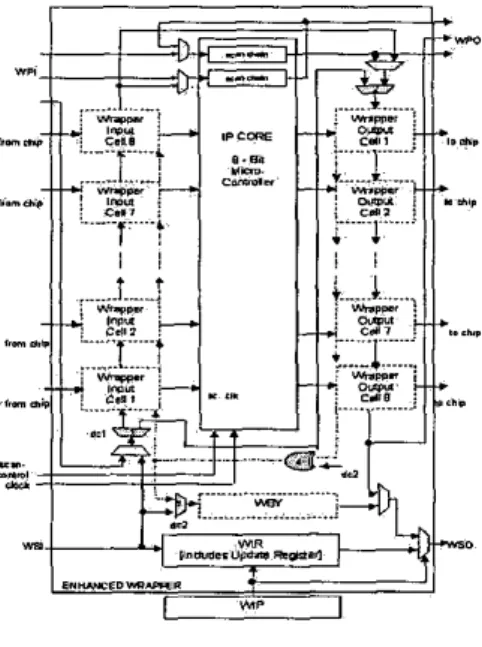
The enhancements to the wrapper are limited lo the addition of two multiplexers, one demultiplexer and an XOR gate. The XOR gate, in figure I number 4, is employed to establish either an inverting or non-inverting feedback Imp.
Flgure 1. Enhanced Wrapper
To be able to have a different select address for the wrapper input and wrapper output cells we need a separate path for the wrapper output cells to be able to load
a different select address than that as for the wapper input cells. This can be accomplished by using a demultiplexer
(I), multiplexer (2) and the use of control signal “del”. The function of multiplexer (3) will be explained in another section. The modified wapper architechre is shown in
figure 1. The shaded elements are new to the wrapper and
the elemmts depicted with a dotted line have been modified in figure 1. The testing for delay faults in the wrapped c m can be done by semitising thc critical path that is required to be tested and selecting the appropriate m p p e r input cell and the wrapper output cell. The test p m e d w together with the extra insbctions that are needed will be explained in the follawing sections. It must be noted that it is assumed that the unique cell addresses me already loaded in the cells address registem The wrapper is therefore in the n m l mode and has no effect on the inputs and output to and from the chip to the core.
The delay testing process makes use of four control signals: dc, dc0, dcl and dc2. The specific use of the signals is as follows:
o o
o
o
de -Allow loading of data into the
CAR
de0-
Select input signal for the WBY dcl - Load address data into the output cellsde2
-
Used to establish either an inverting 01 non- inverting feedback Imp and enabling WBY for countingA dedicated delay test
E‘
core or conk01 unit on the chip can generate these control signals. To control the CAR we define the following instructions to be wriden in the W R Register:o LOADIN-LINIQ: it loads the unique addresses
from WSI into the CAR of all wrapper input cells
LOADOUT-UNIQ: it laads the unique addresses from WSI into the CAR of all wrapper output cells
o
V. RESULTS
WITH
VHDLMODEL
OFBMIANCHED WRAPPER
To be able to verify the operation of the wrapper it is
necessary to manually apply the setup signals and observe the relevant signals of the wrapper. All wrapper elements were clocked by a single clack (WCLQ sipal.
AU
of the insmclions were loaded serially. In the following sections the setup procedures and r e d l of VHDL simulationson
the operation of the enhanced wrapper will be shown. A. Wrapper Cells SelectionThe input cell is primary required for the transport of data &om the chip to the core. The cells also provide access for the scan-in or scan through of data. As explained earlier,
the enhanced cell also has the ability that a unique address
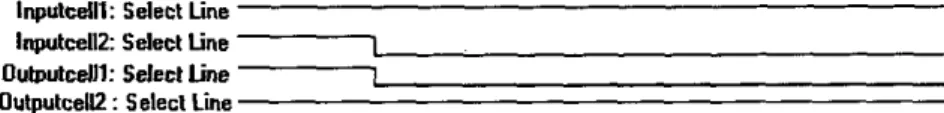
can be stored in the CAR and then be compared with the selection address in the AD for delay fault testing. In figure 4, the timing and signal set- up for &st loading of unique address are shown
The results show that the unique address only gets updated into the CAR fiom the AD once the Up&elYR:
CAR
signal becomes active. The two input cells now have two unique addresses. The same sequence is shown far the output cells and signal del is used to scan in data to the output cells so that the unique address can be loaded faster. Note that an instruction must first be loaded into the WIR and be updated in the WIR to allow the loading of theInpulcelll: Select Line
Inputcelll: Select l i n e
1
o ~ d l l : selectLine
1
Outputcell2 : Select LineFigure 2. Input and Output Cell Select Lines
unique address for the input and output cells. As mentioned earlier, this all can be done while the wrapper is in normal mode. Once the unique addresses
are
loaded into theCAR
of each cell, the cells are ready to be selected for the delay fault test. Only one input and one output cell must be selected The output of the cell will be connected to the delay line (see figure I) and the delay line to the input of the input cell.
This
then provides the feedback loop that is required for the oscillation test method. If an inverting feedback is needed then signal dc2 willprovide it via the added XOR gate in the delay l i e .The first step in the delay fault-testing procedure is to load the selection addresses into the AI) of the cells. There will be one address for the input cells and a different address that will be loaded into the output cells. It is critical that only one input and one output cell is selected for the tesL When the selection addresses are loaded into the
ADS
of the cells, the address will be compared with the unique address of the cell once theC Z
signal gets active.This
willresult in ORIY one input and one output cell select lines to be active. In figure 2, only input cell number 2 and output cell number 1 are selected and therefore their select lines are active. In our example we are using input cell number 2 as thes
m
and output cell number 1 as the end of ow selected critical path through the core. As can be seen in figure 3, once the cells are selected and they are linked from the output cell to the input cell we are able to perform the oscillation test to detect delay faults. The only element in the feedback path that adds to the delay time of the critical path is the XOR gate and the multiplexer on the input cell side (see figure 1) and the buffer on the output cell side.The next stage in the delay-testing prccess is the evaluation of the oscillating frequency. This will be discussed in the next section. For testing purposes the core is represented by a simple combinational circuit.
input1 from -pihC
n
Input1 to C o r e n
n
i
p
n
outputz From C o r e n - -rl I
Input2 from Chip l-r--U
U
UU
UU
UInput2 to C o ~~~ r e r
Outpull from Core
P
flOutpull to Chip outputz to C h i p n
n
-
WCLK W WCI DCO DC1 DCI
Flgure 3. Delay Fault
T
B.
Dehy Fault DetectionThe essential p m of this testing method is the evaluation of the oscillation frequency.
In
the oscillation tee method, the oscillating frequency must be observed to compare it with the oscillation frequency of a good device to be able to detect any extra delay in the selected critical path. Any extra delay will alter the oscillating frequency and can therefore be detected.The
WBY
has been used for the evaluation of Ihe oscillation frequency. This is favourable in order to reduce‘estlng Timing Diagram
the amount of extra elements needed for this proposed testing technique. To be able to use the
WBY
for themeasuring of the oscillation frequency it is necessary that
the WBY
must be able to count this frequency. It therefore requires a register and also a counter. As registers are conskucted by using flip-flops, it will be possible for theWBY to be configured as a counter. The input to the bypass register will therefore be normally shifting data or the oscillation frequency will Mgger it as a counter. Therefore if the WBY is enabled for a certain time period while being triggered by the oscillation frequency a certain counting word will be stored in the WBY &er this time period. This
word will then be relative to the oscillation frequencies. Any extra delay in the selected critical path will alter the oscillating frequency and therefore also the value of the counted word in the
WBY.
The simulation results are shown in figure 3. The results show how the WBY acts as a counter to measure the oscillating frequency. The selection of the input and output cells are similar to that previously explained In figure 3, input cell number 2 and output cell number 1 are selected and the figure clearly shows that the oscillation occurs between these two cells and through the core. Before the oscillation test SMS, the WBY is being reset. Signal dc0 together with de2 enables the
WBY
for a certain time period and it counts the number of pulses f" the oscillating frequency in that time frame. The value in the WBY can be serially shifled out and evaluated on chip or with a slow- speed tester. The WBY can then be used as a bypass register or oscillation counter depending on the instruction in theWIR
together with the WIP signals for bypassing data through the m p p e r . This proves therefore that delay faults, that are a combination of path and gate delays, can be detected with this techniqueThe proposed enhancements were simulated in
ModelSim using an &bit microcontroller core. The enhanced wrapper for the %bit microconholler core is
shown in figure 4. The core was synthesized and the longest delay through the core was measured to be 7.11ns. This delay origktes from input d a b line number 7 through to the address output-line number 15. This shows that for some instances it will be necessary to make use of wapper output cells for intemal signals that are part of the set of critical paths in the core. This was done in the same way that the m p p e r output cells were designed for the primary outputs of the core. We added an extra delay of 4oOps to the path
though the core and the value of the count in the
WBY
has changed from 31 to 35. This indicates that the added delay fault of 400p has been detected. One problem that had to be overcome was that the microprocessor output lines only get updated an the rising edge of the clock pulse. Therefore atest routine was developed to ensure that the output lines were updated constantly to e n s u that the oscillation test method could be used. This test mutine will be activated with the "dcl" control signal
C. Zmpiemenring Test Technique on Sequenriai b g i c In a sequential circuit, the system is free of timing failures if every combinational path between two memory elements propagates its signal in less time than the interval of the operating system clock In other words, the input signal of every memory element in the system should have a stable signal before the arrival of the active clock edge.
A simplified example of a sequential circuit is shown in figure 5. To ensure that the system is fault-free, the clock period should be larger than the sum of the propagation delay of the input flipflop FW (tpm), the propagation delay of the combinational circuit (1-), and the setup time of the output flipflop FFo (tsun.)
[SI.
TCK ? ( tpm + tpm + t s m ) Eqnatlon 1
The above relationship can be rewTitten as follows t m < ( T c r - t r m -tsmo) Equation 2 Therefore a given delay increase in a path may result in a malfunction in the circuit, but the same delay increase in another path may not affect the circuit functionality and p e r f o r m " .
Figure 5. Simple sequentlal clrcuit
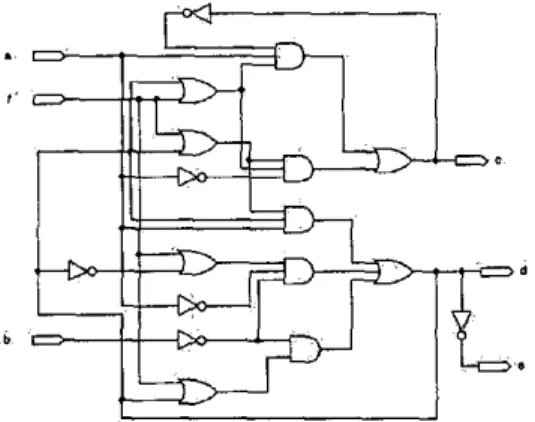
Figure 6 shows a simple sequential circuit containing feedback. The output waveform for this specific circuit under specific input conditions is shown in figure 7. This simulation results indicates the sequential behaviour of the circuit. Figure 8 shows the oscillating output waveform when a critical path in the circuit is sensitized. Dedicated test inputs are used at the circuit's primary input to be able to sensitize the critical path.
This
verifies that the oscillation test method an be applied to sequential circuits with feedback.It is clear from the results that the application of the oscillation test technique to B sequential circuit is viable. Automatic test paltem generators for test sequence
generation in sequential circuits are available and can be use to eliminate the time consuming process of finding correct test patterns for sensitizing the critical paths.
Rgore 6. Sequential Clrcuit used for slmulatlons
75.m imak
Figure 7. Output waveform of sequential eircult during normal operation
Figure 8. Oulpul naveform of sequeulhl rlrcuit
when urlng the o ~ c l l l a l l o ~ test method
v1. CONCLUSIONS
The quest for the detection of delay faults is driven by the increased performance rquirements of VLSI circuits. Our proposed architecture is primarily aimed at the detection of delay faults in embedded cores. Simulation results prove that the proposed enhanced wrapper will be
able to test embedded cores for delay faults.
The enhancements were done to allow delay fault testing of embedded cores without needing much exha chip area. The input cells and output cells were enhanced to allow the cells to be individually selected which is B major advantage to the cells and wrappe. Another advantage is the use of the
WBY
far measuring the oscillation frequency. The proposed enhancements to the PlSOO wrapper will make it possible that delay fault testing of various cores can be done in parallel thereby reducing the test time.The complete enhanced wrapper that includes the input cells and output cells were verified by simulations to ensure correct operation w i t h the PI500 guidelines. An exhhs delay was added in the critical path and the results show that our enhanced wrapper was able to detect this added delay fault. This proposed technique does not require many exha
elements in the wrapper and it still remains PI500 compliant. The possibility to test the external circuitry and interfacing circuitry for delay faults with the use of this architecture will be investigated.
REFEWNCES
[I] EJ Mariohw RKapu, M. busbag, T. Mcburin,M. Rischeni, an3
Y. &"an, ''00 IEEE PISW's Stsndard for Embcddod Cms Ted', J o m c l o/Elmronlc Toting: Theory md.4&cdonr, vol. 18, no. 4 5 , pp. 365- 383, AugsliDctober 2002.
[2]Y. zaian,'7~lR4~-~f,EmbcddsdCarr-Baral
Sy;t- urd IEEE PISOO:' in fiocmdngs IEEE 1nlemmion.d Ten GWfirmc2 (l"CY,Wm~glm~Dc,Nov. 1997,pp. 191-199.
P]
T. McLavln ?ad S. Ghmh," R M I O Incmpamles Hard- SC-U of IEEE PISM", JEEE h i g n & Tert o/ COVUIBS, May-lue 2 0 4w.8- 13.
141 K.T. Lee and IA. Abraham'' Critical Path IdmtiGcaticm and &by Tee of D W c CiMit?, Fmceedhgs a/hnmmiond Tar Con/&xs, 1999,pp. 421430.
[SI M. Mi, H. Ih., C Ixlfaza andB. K m i n h , "Digital Orcillafion-Tcrl Method for &lay and SluEk-at Fault Tcrling ai Digital Clra"ts*, IEEE
lbm-~onr on I n m w " r m ' o n and U - m , Volume: 48 h u e : 4.
[6] EJ Marinisen, S.K. Goel, and M. h w b r g , '?ow& a Slandard fa
Fmbeddd Cme Tat: An Fxample", Pmcoedb@ of Inremnrioml T-I P] H.I. V c dand H.G. KOLhoff, '"Eobmccd PlSW b p l i m l Wmppa ault&lc Crr M a y Favll Tcrbhg of Fmkdded Cam", FTomzdiw qlEumprm Tot Wmhhop. 2033, pp 121-126
AWS 1 9 9 9 , ~ ~ . 798.806.
~ / ~ m I I c c , 2 w o ,