SEU sensitivity and modeling using picosecond pulsed
laser stimulation of a D Flip-Flop in 40 nm CMOS
technology
Cl´
ement Champeix, Nicolas Borrel, Jean-Max Dutertre, Bruno Robisson,
Mathieu Lisart, Alexandre Sarafianos
To cite this version:
Cl´
ement Champeix, Nicolas Borrel, Jean-Max Dutertre, Bruno Robisson, Mathieu Lisart, et
al.. SEU sensitivity and modeling using picosecond pulsed laser stimulation of a D Flip-Flop
in 40 nm CMOS technology. Defect and Fault Tolerance in VLSI and Nanotechnology
Sys-tems (DFTS), 2015 IEEE International Symposium on, Oct 2015, Amherst, United States.
<
10.1109/DFT.2015.7315158
>
.
<
emse-01227355v2
>
HAL Id: emse-01227355
https://hal-emse.ccsd.cnrs.fr/emse-01227355v2
HAL
is a multi-disciplinary open access
archive for the deposit and dissemination of
sci-entific research documents, whether they are
pub-lished or not.
The documents may come from
teaching and research institutions in France or
abroad, or from public or private research centers.
L’archive ouverte pluridisciplinaire
HAL
, est
destin´
ee au d´
epˆ
ot et `
a la diffusion de documents
scientifiques de niveau recherche, publi´
es ou non,
´
emanant des ´
etablissements d’enseignement et de
recherche fran¸
cais ou ´
etrangers, des laboratoires
publics ou priv´
es.
SEU sensitivity and modeling using picosecond
pulsed laser stimulation of a D Flip-Flop in 40 nm
CMOS technology
Cl´ement Champeix∗†, Nicolas Borrel∗‡, Jean-Max Dutertre†, Bruno Robisson§, Mathieu Lisart∗ and Alexandre Sarafianos∗
∗STMicroelectronics, Secure Microcontrollers Division (SMD), 190 avenue Celestin Coq, 13106 Rousset, France
†Ecole Nationale Sup´erieure des Mines de Saint-Etienne, Laboratoire Secure Architectures and Systems (LSAS)
Centre de Micro´electronique de Provence, 880 route de Mimet, 13541 Gardanne, France
‡Aix Marseille Universit´e, CNRS, Universit´e de Toulon, IM2NP UMR 7334, 13397, Marseille, France §CEA Cadarache, 13108, Saint-Paul-lez-Durance, France
Abstract—This paper presents the design of a CMOS 40 nm D Flip-Flop cell and reports the laser fault sensitivity mapping both with experiments and simulation results. Theses studies are driven by the need to propose a simulation methodology based on laser/silicon interactions with a complex integrated circuit. In the security field, it is therefore mandatory to understand the behavior of sensitive devices like D Flip-Flops to laser stimulation. In previous works, Roscian et al., Sarafianos et al., Lacruche et al. or Courbon et al. studied the relations between the layout of cells, its different laser-sensitive areas and their associated fault model using laser pulse duration in the nanosecond range. In this paper, we report similar experiments carried out using a shorter laser pulse duration (30 ps instead of 50 ns). We also propose an upgrade of the simulation model they used to take into account laser pulse durations in the picosecond range on a logic gate composed of a large number of transistors for a recent CMOS technology (40 nm).
Keywords—D Flip-Flop cell, Hardware Security, Photoelectric Laser Stimulation, Single Event Effects, Laser Fault Injection, Electrical Modeling
I. INTRODUCTION
When exposed to a harsh environment in space, high atmosphere or even on earth, integrated circuits (ICs) may undergo soft errors. The related phenomena have been known and studied for more than forty years [1–3]. Among the various existing phenomena, single event effects (SEEs) due to ionizing particles may result in a faulty behavior of the hit circuit. For this reason and in order to cope with the effects of such events, a lot of research work has been devoted to the understanding and mitigation of SEEs. In this context, the use of pulsed-lasers was introduced to emulate SEEs [4], [5]. However, another usage of the pulsed-laser is to intentionally induce faults (as a result of SEEs) in security-dedicated ICs in order to retrieve or modify the secret data they may contain [6], [7]. Fortunately, other techniques introduced by researchers from the radiation community to mitigateSEEs may be adapted to cope with the issue of laser fault-injection. Electrical models have been created in order to propose a fast and simulated analysis (SPICE) of a circuit under laser stimulation. These electrical models make it possible to simulate the response of integrated circuits to laser pulses in very small amount of
calculation times by comparison with physical experiments on laser equipment orTCADsimulation. The novelty of this paper is that our model takes into account very short laser pulse durations with a thin spatial accuracy to identify sensitive areas for a recent CMOS technology (40nm instead of 0.25µmor
90nm).
This paper is organized as follows: Section II describes the principles of laser fault injection. Section III introduces the D Flip-Flop architecture used in our experiments. Hypothesis are made and validated both with experiments (Section IV) and modeling (Section V). Weaknesses and strengths, revealed during the testing, are discussed afterward. A laser pulse duration in the picosecond range for emulating SEEs [5] was used. Then, Section VI draws a conclusion.
II. STATE OF THE ART
ICs are known to be impacted bySEEs caused by ionizing particles in radioactive environments. The related electrical phenomenon and the laser impacts on gates, as latches,SRAM (Static Random Access Memory) or D Flip-Flop, are reviewed in the following subsections.
A. Single Event Effects in Integrated Circuits
When an ionic particle passes through silicon, it generates electron-hole pairs along its path. These electrical charges generally recombine without any significant effect onIC com-putations. However the electric field found in reverse-biased PN junctions may separate the electron-hole pairs, inducing a parasitic transient current. This transient current may in turn disturb the voltage across the IC’s internal nodes, leading to computational errors. A pulsed laser may be used to mimic (or emulate) this phenomenon provided that its photons energy is bigger than the silicon bandgap (electron-hole pairs are then induced by photoelectric effect [4], [5]). At first, pulsed lasers were used to emulateSEEgeneration inICs for radiation hardness evaluation. Since then, they have also been used to induce faults into secure circuits for the purpose of retrieving confidential data stored into these devices [6], [7]. In the following, laser-induced SEEs are described. A laser-induced transient current is then called a ‘photocurrent’ [8–16].
178 978-1-4799-8606-4/15/$31.00 c⃝2015 IEEE
http://dx.doi.org/10.1109/DFT.2015.7315158
Defect and Fault Tolerance in VLSI and Nanotechnology Systems (DFTS),
2015 IEEE International Symposium on
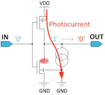
Fig. 1. Laser-sensitive area of aCMOSinverter with its input at low level Fig. 1 illustrates the way how a transient photocurrent is turned intoSEEfor the inverter case when its input is at low logical level. In this configuration, the sensitive SEE area is the drain of the NMOS transistor (shaded in pink), which is in OFF state. A laser-induced photocurrent, depicted by a current source in Fig. 1, may be injected there through the reverse-biased PN junction between the N-type drain of the NMOS (biased at VDD) and the P-type substrate (grounded). As a result of the latter, the inverter output voltage may drop from ‘1’ to ‘0’ provided that the injected photocurrent is higher than the PMOS transistor saturation current. This voltage transient, also known asSET(Single Event Transient), may thus propagate through the circuit logic, creating errors. Note that a similar phenomenon may also take place when the inverter input is at a high logical state (in this instance the laser-sensitive place is the drain of the OFFPMOS): the photocurrent then flows from VDD through the biasing contact (or tap) of the Nwell (i.e. the PMOS bulk) to ground. Furthermore, if a SET is induced directly in a memory element, as a latch, the stored data may be flipped, characterizing the so-called SEU (Single Event Upset; i.e. a bit set from ‘0’ to ‘1’ or a bit reset from ‘1’ to ‘0’).
Fig. 2. Single Event Upset (SEU) description on a latch
Fig. 2 shows the behavior of a latch when aSEUis induced. The increasing or decreasing potential of nodes is symbolized by purple arrows. If the arrow is oriented to the top the potential increases from ‘0’ to ‘1’ whereas if the arrow is oriented to the bottom the potential decreases from ‘1’ to ‘0’. B. D Flip-Flop principles
In an integrated circuit, a D Flip-Flop is a fundamental element for the storage of information and many other uses. A large number of basic Flip-flops cells (more than thousands) can be implemented in circuits, so the protection of these cells becomes mandatory to thwart laser attacks (it has been revealed that a D Flip-Flop is a security weakness point). Our studies on
this basic cell will permit to fine tune the photoelectric model in order to evaluate more complex circuits.
A D Flip-Flop is a memory cell, which memorizes data in an electronic circuit following the truth table in Table I. This cell functions regarding a clock signal. At rising edge on the clock signal, the data in the input of the cell will be in the output but the particularity is to memorize the state when the clock signal is at ‘0’ (non rising).
TABLE I. TRUTH TABLE OF THED FLIP-FLOP
CLK D Qnext Comments
Rising Edge 0 0 Qnext=D= 0
Rising Edge 1 1 Qnext=D= 1
Non Rising X Q Memorizing
C. Memory cells under pulsed photoelectrical laser stimula-tion
Roscian et al. [9], Sarafianos et al. [8], [12] and Lacruche et al. [16] describes the laser sensitivity ofSRAM cells. They also develop an effective model for laser pulse durations above
50ns. Their research permits to identify the critical junctions in a circuit and the importance of the topology (layout) with an old CMOS technology (0.25µm) and a low spatial resolution
(0.5µm). Indeed, long laser pulse durations have not permitted
the precise identification of the sensitive areas (one area was hidden both with experiments and model). Roscian et al. [9] proved that a 1µm spot size was perfect to accurately characterize the sensitive areas. On the other hand, Courbon et al. [17] led his researches on SEUs on D Flip-Flop laser sensitivity but without controlling the clock signal and so without divulging if he impacted the master or slave latch. He demonstrated that he was able to obtain one failure mode by reducing the laser power. Unfortunately the layout recognition were not communicated and the sensitivity junctions was not identified precisely. Indeed the step size of the maps they chose was too high compared to the size of transistors to identify a large amount of gates in his circuit but they were able to identify Flip-Flops and their orientation in a glue logic. In previous works, Lacruche et al. [16] ameliorated the electrical model for picosecond laser pulses based on the comparison of 50ns and a 30ps laser pulse durations of faults on an
SRAM cell in 0.25µm CMOS technology. It has been shown that with a picosecond source the sensitive areas are more distinguishable than with a nanosecond source. Considering their works, we chose to draw accurate maps in order to precisely reveal the sensitive areas by choosing a thin spot size (1µm) and a picosecond source on a recentCMOStechnology circuit (40nm).
To control laser impacts either on the master or the slave latch, the input signals must be perfectly set as it is explained in Fig. 3 and Fig. 4, the test are in static mode. First atCLK=‘0’ the data is not yet in the master latch, it will be transferred and memorized at the rising edge. IfCLKstays at ‘1’, the impacted latch is the master one (Fig. 3a and Fig. 4a) but if theCLKgoes back to ‘0’ the data will be transferred and memorized in the slave latch (Fig. 3b and Fig. 4b).
Fig. 3. Flip-Flop settings with input at ‘1’ in order to impact either master or slave latch
Fig. 4. Timing diagrams of the different configurations of the D Flip-Flop III. ARCHITECTURE OF THED FLIP-FLOP USED IN THE
EXPERIMENTS A. D Flip-Flop architecture
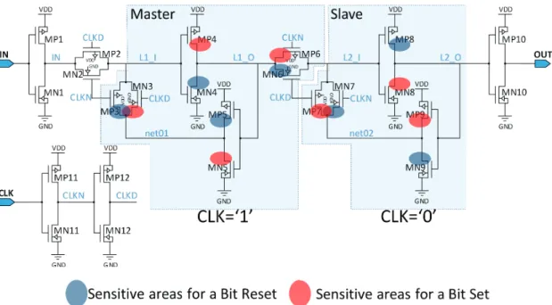
The cell studied in this section of the paper is a D Flip-Flop made of 24 transistors similar to those used in secure integrated circuits (Fig. 6) and based on a basic architecture using two latches: a master latch and a slave one (Fig. 3). There is no reset in that structure in order to simplify the studies by minimizing the number of transistors. Indeed, basically a D Flip-Flop requires several stages: inverting input buffers, two latches, output buffers, clock inverters and asynchronous reset signal. Note that this standalone Flip-flop is embedded in a test chip designed in a CMOS40nm process.
B. Theoretical photoelectric sensitive junctions
In the D Flip-Flop, the fault areas are separated in two parts: master latch and slave latch. Fig. 3 reminds the settings for those both parts in depending on the input signals (Fig. 4). In this subsection, the D Flip-Flop cell sensitivity is studied from a theoretical point of view (considering its schematic and its state).
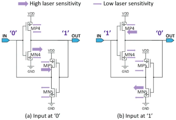
In order to simplify the explanation, the theoretical pho-toelectric sensitive junctions are described on a simple latch. Obviously it is similar for both latches composing the D Flip-Flop. Two cases are considered: input at ‘0’ and input at ‘1’. 1) Input at ‘0’: When the input is at ‘0’, theOUTnode is at ‘1’. Based on [8], [9], [12], [16], [18], the sensitivity of the cell can be investigated by considering whichPNjunctions are the most reverse-biased according to the latch state. Indeed, these
Fig. 5. Schematic of a latch cell laser sensitivity with input at ‘0’ and ‘1’ reverse-biased PN junctions are the place where the electrical field is strong enough to generate a transient current likely to induce an SEU. It is well known that the more reversed-biased the PN junction is the more photocurrent is generated. Based on this fact, we show the photocurrent direction and its strength on Fig. 5a. The purple arrows give the directions of the induced photocurrents between the transistor Drain and bulk or Source and bulk. The thick arrows represent large photocurrents, and the thin arrows smaller ones. The junctions where the photocurrent is the more important are the most sensitive.
Consequently, in Fig. 5a, the two areas most sensitive to laser illumination are the drain junctions of the MN4 and MP5 transistors.
2) Input at ‘1’: When the input is at ‘1’, the OUT node is at ‘0’. Based on the same investigations, the photocurrent direction and its strength are depicted on Fig. 5b. Consequently, the two areas most sensitive to laser illumination are the drain junctions of the MP4 and MN5 transistors.
Therefore, four sensitive areas are expected on the latch: two with the input at ‘0’ and two others with the input at ‘1’. According to the previous paragraphs, fourteen photoelec-trical sensitive D Flip-Flop junctions can be identified, on the schematics and layout (Fig. 6 and Fig. 7), eight on latches and six on pass gates. The blue circles are the areas where laser injection changes the data from ‘1’ to ‘0’ (bit reset) whereas the red circles are the areas where the laser injection changes the data from ‘0’ to ‘1’ (bit set).
IV. EXPERIMENTS A. Device under test
The device under test (DUT), was designed in the 40nm
STMicroelectronics CMOS technology and its core voltage is
1.2V.
To understand the different detection maps reported in sec-tion IV-C, Fig. 7 describes how the transistors are distributed in the layout. The laser maps cover the whole D Flip-Flop (10µm×6µmwith a step size of0.2µm).
Fig. 6. D Flip-Flop architecture with theoretical photoelectric sensitive junctions
Fig. 7. Layout of the D Flip-Flop with theoretical photoelectric sensitive junctions with each transitors referenced
B. Experimental set-up
The fiber laser source used during the experiments pro-duces laser pulses in the picosecond range (30ps pulse du-ration for the test series we reported in this paper). It has a
1030nmwavelength (near Infra-Red), which makes it possible
to access the sensitive areas of a target through its backside (i.e. through its silicon substrate). Our tests were actually performed through the target backside, which was thinned to
∼ 150µm thickness to minimize the amount of power lost
along the laser beam path due to absorption phenomena. The laser beam was focused on theDUT’s sensitive parts: given the
×100optic we used, we obtained a laser spot with a diameter of ∼ 1µm (refer to [5] for a complete description of laser
beam propagation through silicon and beam focusing). Fault maps were drawn to have a spatial representation of the faults
area.
To plot the sensitivity maps, the laser moves thanks to a XYZ stage (accurate to0.1µm) whereas the test chip is fixed. At every point, all the input signals are set with anFPGA, and the acquisitions are captured by a remote oscilloscope.
The experiments are divided into four steps in accordance with Fig. 4. These four cases are reported in Table II. Then the four results are merged in only one maps to simplify visualization and understanding.
TABLE II. TABLE OFD FLIP-FLOP EXPERIMENTAL STEPS Steps number Input (D) Clock (CLK) Comments
Step 1 0 0 Bit set / Slave impacted Step 2 0 1 Bit set / Master impacted Step 3 1 0 Bit reset / Slave impacted Step 4 1 1 Bit reset / Master impacted The laser is shot when all signals are stable (Fig. 3 and Fig. 4). The acquisition of the output needs to be done after a delay, the time need by the D Flip-Flop to change states (a few nanoseconds here because of the capacitor and resistivity of the net and gate delay).
For our experiments, the main objective was to understand the sensitivity maps in order to enhance the electrical model of pulsed photoelectrical laser stimulation (PLS).
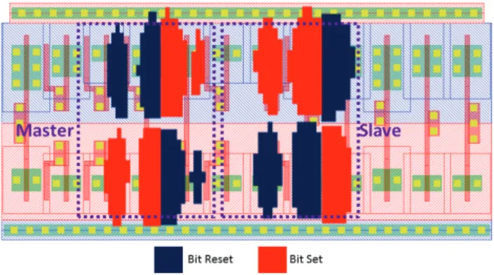
C. Evaluation at0.7nJ laser energy (SEU sensitivity maps) Fig. 8 gives the experimental fault (or sensitivity) map at 0.7nJ laser energy. It shows that the sensitive areas are
the same as the photoelectrical hypothesis ones but exhibits one hidden area (Bit set in the slave latch when CLK=‘0’ and D=‘0’). This hidden area can be explained because of the capacitor onL2_O node. Indeed the transistor Gate-Bulk capacitors of the Buffer/Inverter are bigger than the inverters in
TABLE III. DESCRIPTION TABLE OF TRANSISTORS SIZE RATIO Transistors Ratio W/L Comments MN1, MN10 5 NMOS BUF/INV MN2, MN3, MN6, MN7 3.5 NMOS Pass gates MN4, MN5, MN8 MN9, MN11, MN12 3.5 NMOS INV
MP1, MP10 10 PMOS BUF/INV MP2, MP3, MP6, MP7 3.5 PMOS Pass gates MP4, MP5, MP8 MP9, MP11, MP12 7 PMOS INV
the latch (Table III). Also there is no common junction for the same fault with a pass gate on MN8 transistor so it needs more energy is required for this area to appear. A common junction shared, for the same fault, with two transistors is more sensitive than only one junction.
Fig. 8. Experimental results of a photoelectrical laser stimulation on a D Flip-Flop with a laser pulse duration of30psand a laser energy of0.7nJ
Note that the first faults appear at a laser power duration of0.5nJand the D Flip-Flop has been broken bellow0.9nJ.
V. ELECTRICALMODELING OF THE PULSED PLS The photocurrent generated by a pulsed-laser in an IC is generally modeled by current sources plugged in parallel to its PNjunctions. The electrical models under pulsed laser stimula-tion (N+ on Psubstrate, P+ on Nwell and Nwell on Psubstrate) were previously introduced [10], [11], [13], [15]. We have also already published electrical models, based on these preliminary studies made from measurements and simulations, on basic structures, which create photoelectrical effects. These models use a current source controlled by voltage to model the laser-induced photocurrent. They take into accounts the laser spot size, power, pulse duration, the focus of the laser beam, spatial parameters (location, geometry, wafer thickness) and the PN junction voltage biasing. This is the first electrical stimulation test compared to measurements of a relatively complexCMOS cell in40nm.
A. PNjunction modeling
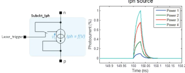
Using the laser beams to study each junction of our structure lets us create PN junctions models (called Sub-ckt Iph diode) which contain a voltage-controlled current source. The amplitude value of this current source is defined byIphas expressed in Eq. 1:
Iph= 1
γ(αV +b)αgaussP ulsewidthWcoefIph z (1)
where, V is the reverse-biased voltage, a and b depend on the laser power,γ is an amplitude attenuation coefficient, αgaussis the sum of two Gaussian functions, which take into
account the spatial dependency,P ulsewidthconsiders the laser
pulse duration dependency,Wcoef is an exponential function
allowing for the wafer thickness effect andIph z is a curve
function which considers the focus effect of the z-axis of the laser lens: αgauss=βe −d2 c1 +ρe −d2 c2 (2) P ulsewidth= 1−e −tpulse 250.10−9 (3) Wcoef=e−0.001W af erthickness (4) Iph z= (c1z6+c2z5+c3z4+c4z3+c5z2+c6z+c7)c8e −z2 20000 (5) where,dis the distance (inµm) between the laser spot and the center of thePNjunction,tpulseis the laser pulse duration
(in second),W af erthickness is the thickness of the wafer (in
µm) andzis the laser lens distance (inµm) withz= 0when
focused on the active area. The other coefficients depend on the CMOS technology and laser lens type. All coefficients values are available and detailled in [10].
Fig. 9. Electrical modeling of aPNjunction under pulsed laser stimulation In order to simulate this photocurrent effect, we built the sub-circuit (see Fig. 9) which contains a voltage controlled current source. Eq. 1 describes the current amplitude of the current source and the laser trigger signal sets the start and duration of the laser pulse. Fig. 9 also represents the simulated photocurrent generated by the model.
B. Modeling results
By upgrading and tuning our model described in Section V, we adjusted the parameters of the photocurrent shape for short pulses. Given that measurements with a 50ns laser
pulse duration showed the absence of bipolar effects, for the modeling we neglected these effects and focused only on photoelectrical effects. The sensitivity map (Fig. 10) was extracted with low energy and a laser pulse duration of30ps. For accuracy purposes we used a step size of0.1µm for the
modeling. At each point of the map, each transistor received a
Fig. 10. Modeling results of a photoelectrical laser stimulation on a D Flip-Flop with a laser pulse duration of30ps
photocurrent on their active area, depending on their position and size.
Fig. 10 shows theSEUs in both the master and slave latches. It corresponds perfectly with the theoretical photoelectrical sensitive junctions (Fig. 7) but presents differences compared to the experiments (Fig. 8). This can be explained by the fact that the model does not integrated the capacitors and the resistivity of each transistor. Our model is based on the classical netlist (created with the schematic) and layout topology but not based on the postlayout simulations because it is currently difficult to merge both netlists but may be possible in future works.
VI. CONCLUSION
This paper reports the analysis of the laser injection of a CMOS40nm D Flip-Flop cell and the upgrading of
photo-electric laser stimulation models. The preliminary conclusion of this theoretical analyze was that there are seven sensitive areas of the D Flip-Flop cell which modify the output from ‘0’ to ‘1’ and seven others for an output state modification from ‘1’ to ‘0’. This conclusion has been verified in practice (except for one hidden area). The topology of the cell has a strong impact on the sensitivity of aCMOSgate. The sensitive areas revealed by measurement cartographies was also confirmed by proper electrical simulations that take into account the topology of the target but without the capacitor and resistors of the nets and transistors (in a future work we will propose a model that will take account of these parameters). The validity of the approach was assessed by the good correlation obtained between electrical simulations (based on SPICE language) and measurements for this advanced CMOS technology node (40nm) which had never been analyzed either in simulation or experiments. This model could permit us to propose and to validate (on simulation basis) a new layout of a standard D Flip-Flop cell more robust against SEU. As a conclusion we can say that the electrical model presented in this paper could be an interesting tool for designers who wants to build CMOSgates more robust againstSEU effects or fault injection in the security field or, who want to test the robustness of their designs.
REFERENCES
[1] D. Binder, E. Smith, and A. Holman, “Satellite anomalies from galactic cosmic rays,”IEEE Transactions on Nuclear Science, vol. 22, no. 6, pp. 2675–2680, Dec 1975.
[2] E. Normand, “Single event upset at ground level,”IEEE Transactions on Nuclear Science, vol. 43, no. 6, pp. 2742–2750, Dec 1996. [3] R. Baumann, “Radiation-induced soft errors in advanced semiconductor
technologies,”IEEE Transactions on Device and Materials Reliability, vol. 5, no. 3, pp. 305–316, Sept 2005.
[4] D. Habing, “The Use of Lasers to Simulate Radiation-Induced Tran-sients in Semiconductor Devices and Circuits,”IEEE Transactions on Nuclear Science, 1965.
[5] S. P. Buchner, F. Miller, V. Pouget, D. P. Mcmorrow, and S. Member, “Pulsed-Laser Testing for Single-Event Effects Investigations,”IEEE Transactions on Nuclear Science, vol. 60, no. 3, pp. 1852–1875, 2013. [6] S. P. Skorobogatov and R. J. Anderson, “Optical fault induction attacks,” in4th International Workshop on Cryptographic Hardware and Embedded Systems, ser. CHES ’02. London, UK: Springer-Verlag, 2002, pp. 2–12.
[7] A. Barenghi, L. Breveglieri, I. Koren, and D. Naccache, “Fault injection attacks on cryptographic devices: Theory, practice, and countermea-sures,”Proceedings of the IEEE, vol. 100, pp. 3056 – 3076, 2012. [8] A. Sarafianos, C. Roscian, J. Dutertre, M. Lisart, and A. Tria, “Electrical
modeling of the photoelectric effect induced by a pulsed laser applied to an SRAM cell,”European Symposium on Reliability of Electron Devices, Failure Physics and Analysis (ESREF), 2013.
[9] C. Roscian, A. Sarafianos, J.-M. Dutertre, and A. Tria, “Fault Model Analysis of Laser-Induced Faults in SRAM Memory Cells,” 2013 Workshop on Fault Diagnosis and Tolerance in Cryptography, pp. 89– 98, Aug. 2013.
[10] A. Sarafianos, O. Gagliano, V. Serradeil, M. Lisart, J.-M. Dutertre, and A. Tria, “Building the electrical model of the pulsed photoelectric laser stimulation of an NMOS transistor in 90nm technology,”IEEE International Reliability Physics Symposium (IRPS), pp. 5B.5.1–5B.5.9, Apr. 2013.
[11] A. Sarafianos, O. Gagliano, M. Lisart, V. Serradeil, J.-M. Dutertre, and A. Tria, “Building the electrical model of the pulsed photoelectric laser stimulation of a PMOS transistor in 90nm technology,” 20th IEEE International Symposium on the Physical and Failure Analysis of Integrated Circuits (IPFA), pp. 22–27, Jul. 2013.
[12] A. Sarafianos, M. Lisart, O. Gagliano, V. Serradeil, C. Roscian, J.-M. Dutertre, and A. Tria, “Robustness improvement of an SRAM cell against laser-induced fault injection,”IEEE International Symposium on Defect and Fault Tolerance in VLSI and Nanotechnology Systems (DFTS), pp. 149–154, Oct. 2013.
[13] N. Borrel, C. Champeix, E. Kussener, W. Rahajandraibe, W. Lisart, A. Sarafianos, and J. M. Dutertre, “Characterization and simulation of a body biased structure in triple-well technology under pulsed photoelectric laser stimulation,”International Symposium for Testing and Failure Analysis (ISTFA), 2014.
[14] C. Champeix, N. Borrel, J.-M. Dutertre, B. Robisson, A. Sarafianos, and M. Lisart, “Experimental validation of a Bulk Built-In Current Sensor for detecting laser-induced currents,”IEEE International On-Line Testing Symposium (IOLTS), 2015.
[15] N. Borrel, C. Champeix, E. Kussener, W. Rahajandraibe, W. Lisart, A. Sarafianos, and J. M. Dutertre, “Electrical model of an NMOS body biased structure in triple-well technology under photoelectric laser stimulation,”International Reliability Physics Symposium (IRPS), 2015. [16] M. Lacruche, N. Borrel, C. Champeix, J.-M. Dutertre, C. Roscian, A. Sarafianos, J.-B. Rigaud, and E. Kussener, “Laser Fault Injection into SRAM cells: Picosecond versus Nanosecond pulses,”IEEE Inter-national On-Line Testing Symposium (IOLTS), 2015.
[17] F. Courbon, J. Fournier, P. Loubet-Moundi, and A. Tria, “Combining image processing and laser fault injections for characterizing a hardware AES,” IEEE Transactions on Computer-Aided Design of Integrated Circuits and Systems, vol. 0070, no. c, pp. 1–1, 2015.
[18] L. H´erivaux, J. Cl´edi`ere, and S. Anceau, “Electrical Modeling of the Effect of Photoelectric Laser Fault Injection on Bulk CMOS Design,”
International Symposium for Testing and Failure Analysis (ISTFA), 2013.