June 2008
Tore Marvin Undeland, ELKRAFT
Marta Molinas, ELKRAFT
Master of Science in Energy and Environment
Submission date:
Supervisor:
Co-supervisor:
Control of Multi-terminal VSC-HVDC
Systems
Problem Description
The North Sea has a vast amount of wind energy with largest energy per area densities located about 100-300Km of distance from shore. Should this energy be tapped by offshore wind farms, HVDC transmission would be the more feasible solution at such distances of subsea transmission. On the other hand Norwegian oil/gas platforms in the North Sea use electricity from gas fired turbines at offshore sites. These gas turbines have much less efficiency than onshore generation of electricity and also release large amounts of green house gases. Therefore supplying the platforms with power from onshore transmitted by HVDC will result in benefits both from economic and environmental protection perspectives.
Given these two interests for HVDC in the Norwegian offshore, the use of Multiterminal HVDC (MTDC) is a potential solution for the integration of the wind farms and oil/gas platforms into the onshore grid.
Control systems for multiterminal HVDC (MTDC) networks should be developed and their
operation be analyzed. First controllers for two-terminal HVDC connected to different types of AC grids must be developed and analyzed. Then this must be extended to develop control of
multiterminal HVDC system. Models should be developed in PSCAD/EMTDC simulation software and results should be analyzed to validated proposed control schemes.
Assignment given: 22. January 2008
Table of Contents
Abstract ………..…v Acknowledgements………..vii Acronyms……….viiiChapter 1: Introduction
……….………..…..1 1.1 Background ………11.2 MTDC for Offshore Wind Farms in the North Sea ……….……..3
1.3 Scope of the Thesis Work ……….….4
Chapter 2: Operating Principles of VSC-HVDC
…...……….52.1 Types of Power Semiconductors ……….………..5
2.2 Understanding VSCs………...6
2.3 PWM Techniques………..12
2.3.1 Sinusoidal PWM………...12
2.3.2 Optimized PWM………...12
2.3.3 Space Vector PWM (SVPWM)……….………...13
2.3.1 Sinusoidal PWM with Third Harmonic Injection…………...15
2.4 Two Level and Multilevel Converters………..…16
Chapter Three: Modeling of Multiterminal VSC-HVDC System
..…..…183.1 Introduction………..18
3.2 Design of VSC-HVDC……….18
3.2 MTDC Feature Development………...21
3.3 Types of AC Networks……….21
3.4 VSC-HVDC Terminal Control Configurations………22
3.5 Synchronous d-q Reference Frame………..24
3.6 Phase Lock Loop………..28
3.7 P.U. System………...29
3.7 Convention for Direction of Current and Power Flow……….30
Chapter 4: Control Strategy
………314.3 Control of VSC-HVDC Connected to Active AC Network……….36
4.3.1 Active Power Control………...………….38
4.3.2 Reactive Power Control……….39
4.3.3 DC Voltage Control…………...………...40
4.3.4 AC Voltage Control………...41
4.3.5 Frequency Control………..……….43
4.4 Control Loop Transfer Functions……….44
4.4.1 TF of Inner Current Loop………....………….….44
4.4.2 TF of DC Voltage Control Loop……….45
4.4.3 TF of Active / Reactive Power Control Loops………..……….45
4.4.4 TF of AC Voltage Control Loop for Weak Grid Connection………46
4.4.5 TF of AC Voltage Control Loop for Passive AC Network………...……46
4.5 Tuning of PI Controllers………..47
4.5.1 Modulus Optimum Criterion……….……….47
4.5.2 Symmetrical Optimum Criterion……….………...48
4.6 Control of Multiterminal VSC-HVDC (MTDC)………51
4.6.1 MTDC Control by DC Voltage Margin………...51
4.6.2 MTDC Control by DC Voltage Droop………...….56
4.7 DC Overvoltage Controller………59
Chapter 5: Simulation Studies 5.1 Specification of the VSC………62
5.2 P.U. Calculations………64
5.3 Simulation of Inner Current Loop………..68
5.4 Simulation of Active & Reactive Power Controllers……….70
5.5 Simulation of DC Voltage Regulator……….73
5.6 Simulation of AC Voltage Control for Weak Grid Connection……….75
5.7 Simulation of AC Voltage Control for Passive AC Network………….77
5.8 Simulation of Frequency Control………81
5.9 DC Overvoltage Controller……….82
5.10 Simulations of MTDC Systems………83
5.12 Simulation of MTDC with Voltage Margin and DC Droop Control…88
Chapter 6: Conclusions and Suggested Future Works……….92
6.1 Conclusions………92
6.2 Suggested Further Works………...93
References………94
Appendix………..96
Abstract
The North Sea has a vast amount of wind energy with largest energy per area densities located about 100-300Km of distance from shore. Should this energy be tapped by offshore wind farms, HVDC transmission would be the more feasible solution at such long subsea distances. On the other hand Norwegian oil/gas platforms in the North Sea use electricity from gas fired turbines at offshore sites. These gas turbines have much less efficiency than onshore generation of electricity and also release large amounts of green house gases. Therefore supplying the platforms with power from onshore transmitted by HVDC will result in benefits both from economic and environmental protection perspectives.
Given these two interests for HVDC in the Norwegian offshore, the use of Multiterminal HVDC (MTDC) is a potential solution for the integration of the wind farms and oil/gas platforms into the onshore grid system. Hence, this thesis focuses on the operation and control of MTDC systems. The MTDC system is desired to be capable of interfacing with all kinds of AC grids namely: stiff, weak and passive grid systems.
Compared to the classical thyristor based converter, VSC has several features that make it the most suitable converter for making of MTDC, the most decisive being its ability of bidirectional power transfer for fixed voltage polarity. VSC-HVDC is also suitable for implementing control of active and reactive current in synchronously rotating d-q reference frame which in turn results in decoupled control of active and reactive power.
In the first two chapters of the thesis literatures are reviewed to understand operation of VSC and its use in HVDC systems. Afterwards controllers are developed for different AC connections (stiff, weak and passive) and for different DC parameter (power, DC voltage) control modes. DC voltage and active power control are implemented by active current control and AC voltage and reactive power control are achieved by reactive power compensation. Tuning techniques for the PI controllers are discussed and used in the simulation models. Finally control techniques for reliable operation of MTDC are developed. In order to validate theoretical arguments, each of the control schemes was developed and simulated in PSCAD/EMTDC simulation software.
Simulation results indicate that satisfactory performance of VSC-HVDC was obtained with the proposed active/reactive power controllers, AC/DC voltage controllers, frequency and DC overvoltage controllers.
For coordinated multiterminal operation, voltage margin control method and DC voltage droop characteristic were used. These are control methods based upon realization of desired P-UDC
characteristic curves of converter terminals.
Four-terminal MTDC system with different AC grid connections was used to study the multiterminal operation. Simulations have shown that voltage margin control method results in reliable operation of MTDC during loss of a terminal connection without the need for communication between terminals. The use of DC voltage droop control along with voltage margin control enabled load sharing among VSC-HVDC terminals in DC voltage control mode according to predetermined participation factor.
Acknowledgements
First of all I would like to express my gratitude for Professor Tore Undeland, my supervisor in this thesis work, for giving me the opportunity to explore an interesting field of power engineering with major practical relevance and for his guidance.
I gratefully acknowledge Professor Marta Molinas, my co-supervisor in the thesis work, for her encouragement and guidance during the thesis work. I like to mention that the article which I wrote in connection to this thesis work and presented on NORPIE-2008 conference would have not been a success without her initiative idea and guidance.
I would like to acknowledge PhD students Arkadius Kulka, Jon Are Wold Suul and Samson Gebre for their co operations in solving difficulties with using PSCAD simulation software package and giving technical suggestions.
I would like to thank my friends at the Department of Electric Power Engineering for creating a friendly and productive working environment.
Acronyms
AC alternating current
DC direct current
HVDC high voltage direct current VSC voltage sourced converter PWM pulse width modulation
SV-PWM space vector pulse width modulation MTDC multiterminal HVDC
FACTS flexible AC transmission system IGBT insulated gate bipolar transistor IEGT injection enhanced gate transistor GTO gate turnoff thyristor
IGCT integrated gate commutated thyristor GCT gate commutated turnoff thyristor PCC point of common coupling
Chapter 1
Introduction
1.1 Background
Advancement in production technology of semiconductors and control systems has brought a new era of multifarious applications for power electronic devices. One such application that has become an important element in the modern electric power industry is High Voltage Direct Current (HVDC) transmission technology. Although the first commercial HVDC link was used for submarine power transmission, it has also been in use for the purpose of reducing transmission losses in long distance power links and interconnection of asynchronous power grids.
The earliest HVDC system used mercury valves which, on the advent of power semiconductor technology, were subsequently replaced by thyristor valves. The thyristor based HVDC system, also called classical HVDC, is currently superior in transmitting maximum bulk power for long distances and in a given right of way corridor [1]. With the price of thyristors decreasing and their voltage and current ratings increasing, it is expected that classical HVDC will remain dominant in point to point long distance and submarine bulk power transmission.
Although the classical HVDC has the aforementioned advantages, the need for active network connection at both ends (and hence its inability to supply passive loads), its consumption of reactive power at both terminals, its inability to reverse the direction of current flow, and its susceptibility to commutation failures have been the down sides of classical HVDC. These constraints have limited the use of classical HVDC to power transmission between two points. In the light of this understanding, Voltage Sourced Converter - HVDC (VSC-HVDC), a recent arrival in the arena of high voltage technology, has eliminated all the mentioned drawbacks of
classical HVDC and opened new application areas and possibilities. VSC-HVDC consists of three phase switch mode converter and uses pulse width modulation (PWM) for controlling its phase voltages.
Since VSC-HVDC does not need changing its DC voltage polarity for either direction of power flow and is capable of independent control of active and reactive power flow, it has attracted attention as a promising candidate for developing Multiterminal HVDC (MTDC) system. MTDC is a DC equivalent of AC grid which will have DC transmission network connecting more than two AC/DC converter stations. The range of operating voltage of the DC transmission is expected to be with in specified upper and lower limits. The upper limit of the operating DC voltage can be determined by the ratings of the DC cables, DC circuit breakers or the forward blocking capacity of the IGBTs used in the VSC. The lower limit of the operating DC voltage is determined by the maximum of the operating AC voltages of all the converter stations incorporated in the MTDC system.
If the upper limit of the operating voltage is exceeded, there could follow equipment failure and perhaps subsequent blackout. When the DC operating voltage becomes below the minimum limit, one or more of the VSC-HVDC stations go into 'saturation' condition due to over modulation and the VSC-HVDC terminal will no more respond properly to the controllers.
In practice, the upper and lower voltage limit settings of the MTDC should have sufficient safety margins from the previously mentioned limits.
It is desirable that:
1. The DC voltage of the MTDC should be free from oscillations during disturbances and fault occurrences on the AC sides of the VSC-HVDC stations.
2. Each terminal is capable of independent control of active and reactive power, AC voltage support and frequency droop control as per the need.
With these requirements fulfilled, each VSC-HVDC station will act as inertia-less synchronous machine in the sense that there is almost no delay in the power control response. This is a feature useful in stabilizing the AC system connected to the VSC-HVDC terminal during disturbances.
Another interesting feature is, unlike with synchronous generators, it is possible to implement negative sequence voltage control with VSC-HVDC. This is useful in phase voltage control of the three phase system in unbalanced conditions.
During isolated operation, VSC-HVDC terminal can serve as STATCOM to supply reactive power to the AC system.
1.2 MTDC for Offshore Wind Farms in the North Sea
One interesting potential for application of MTDC in Norway is to interconnect offshore wind farms and oil/gas platforms into the national grid onshore. The offshore wind energy of Norway is said to surpass the nation's current production of hydropower. This vast amount of energy resource, together with the remoteness of the area from public sight, has stimulated research works towards developing offshore wind farms in the North Sea.
Although the challenges of developing offshore wind farms in the deep sea are enormous, equally balanced by the interest for harnessing the energy resource out there and increasing energy price, it is expected that realization of commercial offshore wind farms in the deep North Sea will be a near future [2]. Many of these sites of vast wind energy potentials are located 100-300 Km from onshore [2]. For reasons of large capacitive currents HVAC will likely not be a technically and economically feasible solution for such submarine distances. This makes HVDC the more feasible solution in this particular case.
On the other hand the Norwegian oil and gas platforms, which currently use gas turbines except in one case [15], contribute towards a large share of the total CO2 emission in Norway [16]. For economic and environmental protection reasons there has been a tendency towards replacing the gas turbines with electric supply from onshore grid.
An interconnection between the offshore wind farms, the platforms and onshore grid results in reduced operational costs, increased reliability and reduced CO2emissions. MTDC network will then be the core of such an interconnection system. MTDC can also open new power market
opportunities and result in better utilization of transmission lines [17]. A schematic of MTDC interconnecting an offshore wind farm, offshore oil/gas platform and onshore grid system is shown in Figure 1.1.
Figure 1.1: Proposed interconnections for offshore oil/gas platform, offshore wind farm and onshore grid.
1.3 Scope of the Thesis Work
This thesis work focuses on operation and control of MTDC system based upon VSC terminals. MTDC is a fairly new field of research and so far there is no MTDC system in commercial operation by the time this thesis was written. Operating MTDC system in all possible scenarios of AC connections (passive load, weak grid and stiff grid) and with different controls of DC parameters (constant power, constant DC voltage) must be investigated. Hence VSC-HVDCs connected to the various types of the AC grid systems will be established and control systems developed. Finally the proposed control techniques together with the MTDC models will be simulated in PSCAD/EMTDC software to analyze the steady state and dynamic responses. Simulation results should validate proposed control schemes and show the possibility of building MTDC with VSC terminals.
Chapter Two
Operating Principles of VSC-HVDC
2.1 Types of Power Semiconductors
Semiconductor devices that are used for power electronic applications such as HVDC and Flexible AC Transmission Systems (FACTS) are classified into uncontrolled, half-controlled and fully controlled semiconductors depending upon the controllability of their ON and OFF states. Power diodes belong to the uncontrolled semiconductor devices category where as thyristors are in the half-controlled group since their switching-on is controlled. Fully-controlled semiconductors allow controlling both switching-on and switching-off. Hence the term ‘switch’
in power electronics often refers to the fully controlled semiconductor devices.
Although power transistors are the most common types of switches, there are also special types of fully controlled thyristors that belong to the same group [3]. Below is a summary of fully-controlled high power semiconductors.
Table 2.1 Summary of fully-controlled high power semiconductors
Acronym Type Full name
IGBT Transistor Insulated Gate Bipolar Transistor IEGT Transistor Injection Enhanced Gate Transistor GTO Thyristor Gate Turnoff Thyristor
IGCT Thyristor Integrated Gate Commutated Thyristor GCT Thyristor Gate Commutated Turnoff Thyristor
Since the voltage rating of a single semiconductor device would be too small as compared to the voltage levels of HVDC transmission, several tens of them will be stacked in series and in parallel and controlled simultaneously to achieve the required voltage and current ratings respectively.
2.2 Understanding VSCs
The operating principles of VSC can be understood by tracking its topology back to the simplest switch mode DC-DC converters: namely step-down (Buck) converter and step-up (Boost) converters. Switch mode refers to the high frequency switching of the electronic valves involved in the energy conversion process. Step-up and step-down DC-DC converters are shown in Figure 2.1. A rigorous discussion of these DC-DC converters is found in [3].
Figure 2.1: Schematics of step-down (Buck) and step-up (Boost) converters
Note that in Figure 2.1 the step-down and step-up converters convey power in opposite directions.
In order to conduct current, the switches in the converters must be forward biased in addition to providing the pulse width modulated signals to the switch gates. When the switches are forward biased, the voltages relations will be given by:
Vd =DV1 o (2.1)
o V
for the step-down converter and
for the step-up converter respectively.
D1 and D2 are duty ratios of the switches in the step-down and step up converters respectively. The duty ratio of a switch is defined as the ratio of its ON-state time during one cycle to one period of the switching frequency.
on s T D T = (2.3) And s 1 s T f = (2.4)
where fs is the switching frequency.
This relation is shown in the following diagram.
Figure 2.2: Duty cycle of a switch
The biasing of the switches depends on the difference of the Thevenin’s equivalent voltages of the external networks connected on the left and right sides of the converter.
If the gates are reverse biased while supplied with the switching pulses, there will be no current flow and the input-output voltage relations given by equations (2.3) and (2.4) will no more hold true.
Since the step-down and step-up converters transfer power only to the left and to the right sides respectively, it would be possible to combine the two to make a bidirectional DC to DC converter as shown in Figure 2.3.
Figure 2.3: Bidirectional DC-DC converter
Equations (2.3) and (2.4) must be equal for continuous bidirectional power conversion.
(
)
(2.5) 1 2 2 1 1 1 d o o V DV D V D D = = − → = −Equation (2.5) indicates that T+ and T- are complementary; meaning when T+ is in ON-state
T-will be in OFF-state and vice versa. Hence only one PWM signal generator is needed for both switches of the bidirectional converter.
After rearranging the switches and splitting the DC capacitor into two, we get the following topology shown in Figure 2.4.
Figure 2.4: Rearrangement of the bidirectional DC-DC converter
We define the phase voltage as the voltage of point X with reference to the ground.
(
)
1 1 2 2 2 1 2 DC ph d DC DC DC V V V V D V V D − = + − = + = − , 0≤D1≤1 (2.6) Assigning K=2D1 - 1, 2 DC ph KV V = , − ≤1 K1≤1 (2.7)By varying the constant K, it is possible to interface different levels of DC voltages of the same or opposite polarities for bidirectional power flow.
If we now replace the constant K with a sinusoidal function of variable amplitude, we can get sinusoidal phase voltage (Vph).
In time domain, sin( ) 2 DC a ph V m wt V = (2.9)
And in phasor domain,
l 0 2 2 o a DC ph m V V = ∠ , (2.10)
Where ma is the amplitude modulation ratio and is between 0 and 1.
The bidirectional converter together with the sinusoidal PWM consist the half bridge single phase switch mode converter [3]. Three of the half bridge single phase converters connected in parallel and with sinusoidal modulation signals of 120o apart from each other constitute the three phase switch mode converter, also known as Voltage Source Converter (VSC).
The phrase ‘Voltage Source’ refers to the fact that the polarity of DC voltage in VSC is fixed for both rectifier and inverter mode of operations. For thyristor based converters, it is the polarity of current which is fixed for both modes of operations. The three phase bidirectional converter (VSC) is shown in Figure 2.5.
The ratio of the frequency of the modulating signal (fs) to that of the frequency of fundamental AC component (f1) is called frequency modulation ratio (mf) and is given by:
1 s f f m f = (2.11)
If this ratio is small (<21), mf must be chosen to be an odd integer in order to get an odd symmetry ( f(-t) =-f(t) ) as well as half wave symmetry ( f(-t)=-f(t+T1/2) ), where T1=1/f1. By doing so only odd harmonics of sine terms will be found in the phase voltages of the VSC.
In three phase systems, only harmonics in the line-to-line voltages are of concern. Considering the mf th harmonic, the phase difference between harmonics in phase A and phase B is (mf*120o). Choosing mfas a multiple of three will make this phase difference equivalent to zero (a multiple of 360o). The same treatment applies for the mf+/- j, harmonics with j = odd positive integer. Choosing mf=3 will create harmonics near to the fundamental frequency and result in very large voltage distortions. Hence the minimum recommended value for mf is 9. The zero sequence harmonics occurring in the phase voltages are usually eliminated by a ∆ connected or ungrounded Y connected transformer. The transformer is usually an integral part of VSC-HVDC and contributes to the series inductance (L filter) needed for AC current smoothening.
For very large values of mf (>21) the sub-harmonics due to asynchronous modulation will be small and mf can be assigned non-integral values.
2.3 PWM Techniques
There are several PWM techniques used for VSCs. The simplest one, which also was assumed in previous discussions about VSC, is the pure sinusoidal PWM.
2.3.1 Sinusoidal PWM
Sinusoidal PWM generates pulse width modulated signal by comparing the instantaneous magnitude of a triangular waveform with sinusoidal input reference. This is shown in Figure 2.6.
Figure 2.6: Pure sinusoidal PWM with mf=9
Optimized PWM (OPWM), Space Vector - PWM (SVPWM) and Sinusoidal PWM with Third Harmonic Injection are other types of PWM techniques used for VSCs.
2.3.2 Optimized PWM
This is used for selective harmonic elimination by pre-calculated waveform of PWM. It can also be arranged to minimize the number of switchings around the instant of maximum current flow. This results in reduction of power loss as compared with the simple triangular carrier wave PWM, but also has the disadvantage of computational complexity and variable switching frequency changing with operating conditions.
Figure 2.7: Harmonic spectrum of optimized PWM [7]
2.3.3 Space Vector PWM (SVPWM)
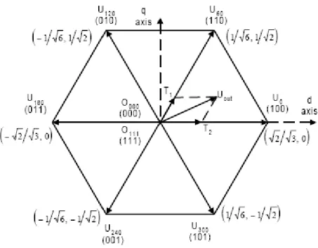
This type of modulation has an objective of minimizing the number of switchings there by reducing switching losses. SVPWM also results in better utilization of the DC bus by increasing the available output voltage by approximately 15% (i.e. to UDC√3/2) compared to the sinusoidal PWM, which gives a maximum phase voltage amplitude of UDC/√2 [5]. In this type of modulation the reference voltage is mapped into switching space vector diagram and the duty cycles of the switches will be calculated based on the mapping.
Table 2.2 Table of IGBT Switchings Status of Switches Output Voltage Vector TA+ TB+ TC+ U0 1 0 0 U60 1 1 0 U120 0 1 0 U180 0 1 1 U240 0 0 1 U300 1 0 1
Figure 2.8: Switching map of SVPWM
Uout in Figure 2.8 indicates the required output voltage phasor in d-q reference frame. In order to calculate the duty ratios of the voltage vectors that generate Uout, the sector where Uout lies should first be identified. Once this sector is found, the duty cycles are calculated from the voltage-time balance during one switching period (Tw).
When Uout lies in the first sector (0<θ<60o):
0 1 0 2 6 3 1 2 ( 0 ) ( ) 2 j sw out sw j DC sw T U e T d d U d U U T d d e θ π = + + = + 0 , d0+ +d1 d2 =1 (2.12)
where d0, d1 and d2 are duty cycles of 0, U0 and U60 voltage vectors. Equating the direct and quadrature axis components,
1 0 2 2 1 cos 2 3 sin 2 out out U d U U d θ θ = + = d (2.13) Hence, 2 1 0 1 2 2 sin 3 1 ( 3 cos sin ) 3 1 out out d U d U d d d θ θ θ = = = − − − (2.14)
The corresponding switching patterns are shown in Figure 2.9.
Figure 2.9: Switching pattern for Uout in U0 – U60
2.3.4 Sinusoidal PWM with Third Harmonic Injection
This type of PWM uses injection of third harmonics in to all the three phases to increase the size of maximum available line to line voltage vector.
2.4 Two Level and Multilevel Converters
The VSC considered so far has only two levels of instantaneous AC voltage (i.e. +UDC and -UDC). Hence this type of VSC is called a two level VSC as opposed to multilevel VSCs that have more than two instantaneous voltage levels.
Multilevel converters have the advantages of [7]:
1. Fewer switching operations for similar harmonic performance 2. Lower voltage per switches
3. Lower power loss
The switching patterns for two level and three level converters are shown in Figure 2.10 below.
Figure 2.10: Switching patterns for two-level and three-level VSCs respectively [7]
There are three topologies of multilevel converters, namely: diode clamped, flying capacitor clamped and cascaded multilevel converters. The following diagram depicts these three topologies of multilevel VSCs.
Figure 2.11: One-leg five-level multilevel topologies: a. Diode clamped, b. Flying capacitor clamped, c. Cascaded H-bridges
Detailed comparisons of the advantages and disadvantages of the different topologies of multilevel VSCs are discussed in literature [6].
Chapter Three
Modeling of Multiterminal VSC-HVDC
System
3.1 Introduction
VSCs have vast areas of applications ranging from small electric drive systems to high voltage DC transmission systems (referred in this paper as VSC-HVDC). VSC has two degrees of freedom, namely the amplitude modulation index (ma) and the phase displacement (φ). In comparison, thyristor based converter has only one degree of freedom, i.e. the firing angle (α). Degree of freedom refers to the number of independently alterable parameters and is an indication of the maximum number of independently controllable output quantities. This higher flexibility together with its fixed voltage polarity for both rectifier and inverter modes of operation make VSC-HVDC the core component in developing MTDC. This chapter discusses design of VSC-HVDC, features of MTDC, types AC buses, and also establishes methodologies to be used in modeling of MTDC system.
3.2 Design of VSC-HVDC
The VSC-HVDC that will be considered in this paper is a two level VSC with pure sinusoidal PWM. Although in practice a converter leg consists of a package of several semiconductors connected in series and in parallel, in the VSC modeling of this paper single IGBT and diode components with very high voltage ratings will form the anti-parallel connections. In addition protection circuits (Snubbers) are not considered in the VSC models.
Design specifications will be made for one VSC and will be used for all VSC-HVDC terminals throughout this thesis work. It should be noted that although the same VSC-HVDC design will be
used consistently, different control strategies will be employed depending on the requirement for control objective at hand. Configuration of VSC-HVDC is shown in Figure 3.1.
Figure 3.1 Configuration of VSC-HVDC
Current Smoothening Inductance (L filter)
As it was discussed in Chapter 2, a series inductance is used for smoothening of the phase currents. The inductance is calculated as.
( h o h V L Max h Iω = ) (3.1)
where Vh is harmonic voltage determined from voltage harmonic table for sinusoidal PWM, Ih is the amount of acceptable harmonic current and h is the harmonic number.
Transformer
Usually, the converters are connected to the AC system via transformers. The transformer has the main purpose of transforming the AC voltage in to a level suitable to the converter. Transformers usually have a leakage inductance between 0.1 - 0.2 p.u. [4].
Phase reactors
Part of the series phase inductance required comes from the transformer (if there is any) and the rest of it is provided by series connected phase reactors.
AC filters
In addition to the series inductance, AC filters can be used to eliminate the voltage harmonics entering into the AC system. The AC filter is a shunt connected high pass filter tuned in the order of the PWM frequency.
(a) (b)
Figure 3.2: Passive high pass filters: a. Second order filter b. Third order filter
DC Capacitors
The use of PWM in VSC results in current harmonics occurring in the DC side of the VSc-HVDC. These current harmonics in turn causes ripple on the DC side voltage. The use of shunt connected capacitor filters out such ripple and results in smoother DC voltage.
While on one hand the use of DC capacitors improves the steady state performance, the dynamic response during disturbances (fault occurrence, load switching) will suffer if capacitors of too large size are used. Therefore both steady state and dynamic response performances should be considered in selecting the size of the DC capacitor.
Hence a time constant, defined as the ratio of the energy stored in the capacitor at rated DC voltage to the rated apparent power of the converter is used for specifying the capacitor size [4].
2 2 DC n CU S τ = (3.2)
into consideration, a time constant of not less than 5 ms was suggested in literature [4].
DC Cables
The shunt capacitance, shunt resistance and series inductance of the DC cables are neglected. Only the series resistance of the DC cable is modeled as a lumped resistive element.
3.2 MTDC Feature Development
Before starting with modeling of MTDC, it is necessary to describe the expected basic features of MTDC system.
An MTDC is expected to consist of several VSC-HVDC terminals connected to each other by DC network. The MTDC should work with a fixed DC voltage level or with in a small window of upper and lower limits. Each of the terminals should be able to adopt different control strategy depending upon terminal specific needs. VSC-HVDC should monitor and control DC side parameters as well as AC side parameters.
3.2.1 DC bus parameter control
On the DC side, the VSC-HVDC may operate in constant DC voltage mode, constant power mode, or constant DC current mode [8]. When the VSC-HVDC is supplying power to passive load, none of the DC parameters is controlled.
3.2.2 AC bus parameter control
On the AC side, the VSC-HVDC may operate in constant AC voltage mode or constant reactive power mode depending on the type of the grid connection. Frequency droop can also be added optionally in the AC bus control.
3.3 Types of AC Networks
AC networks are classified as strong (stiff) grid, weak grid and passive network depending on the stiffness of the AC voltage at the point of common coupling (PCC).
When an AC connection is said to be stiff grid, it means that the AC voltage at the PCC remains constant irrespective of the magnitude and direction of active and reactive power flow.
Weak grid on the other hand has its AC voltage at PCC changing with power flow. This happens due to significant resistive voltage drop across transmission line and is usually associated with long transmission lines.
The AC voltage in passive network is totally dependent on the voltage output of the VSC, hence the name passive network.
In this paper stiff grid is modeled by ideal three phase AC source with constant voltage where as weak grid is represented by ideal three phase AC source in series with line inductance and resistance. Passive network is modeled by resistive and inductive loads.
3.4 VSC-HVDC Terminal Control Configurations
The maximum possible number of controllable output quantities depends on the number of available degrees of freedom. The parameters to be controlled at a terminal should be capable decoupling or at least should be weakly correlated. As discussed before there are three types of AC grid connections, namely passive network, weak grid and stiff grid systems. According to the characteristics of the AC network, VSC-HVDC terminals can be classified in to two major categories.
a. VSC-HVDC for Passive AC network
When the VSC-HVDC is the only source in the AC network it is connected to, the network is said to be passive network. In this type of network connection, the only control objective of the VSC-HVDC is to maintain constant AC line-line voltages.
b. VSC-HVDC for Active AC Network
When VSC-HVDC is connected to active AC network, like in the passive network case, AC voltage at PCC should be kept constant. If the AC connection is stiff grid, the AC voltage level will be constant (stiff) by itself and the VSC-HVDC terminal controls reactive power flow from
the AC side. On the other hand if the connection at PCC is a weak grid connection, the AC voltage should be controlled by reactive power compensation. By considering weak and stiff grids types of connections and constant active power or constant DC voltage control modes, we can get four different control modes of VSC-HVDC terminals, i.e. constant P-VAC terminal, constant VAC-UDC terminal, constant P-Q terminal, and constant Q-UDC terminal.
Hence, the different control modes in passive and active network connections give rise to five possible types of VSC-HVDC terminals.
Type 1: Constant AC voltage for passive network (VAC control)
When feeding power to passive network, the control objective becomes to maintain a constant level of AC voltage at the point of common coupling (PCC). The active and reactive power flows is dependent on the passive network components and therefore are not decoupled. Since there is only one source of AC voltage, there will be no need for frequency control.
Type 2: Constant P- VAC control
P-VAC control is applied when the VSC-HVDC terminal is connected to a weak grid while constant power flow is needed. Since the AC voltage of a weak grid is not constant by itself, it should be maintained to a constant level by the VSC. Active power flow controller maintains constant power flow via the HVDC. The reference input for the power controller may come from a central power dispatching station or can be manually set by operators at site.
Type 3: VAC - UDC control
This is used when VSC-HVDC connected to a weak grid is required to maintain constant DC voltage level. The AC voltage as well as the DC voltage must be regulated by the VSC. As will be shown later on, AC voltage is controlled by reactive power compensation and DC voltage is regulated by active power compensation.
Type 4: P-Q control
This is used when a stiff AC grid is connected to the VSC-HVDC and when constant power control mode is required. Active and reactive powers have their own references and will be
independently controlled. If there is no requirement for control of reactive power flow, Qref will be assigned a value of zero.
Type 5: Q- UDC control
When the VSC-HVDC terminal is connected to a stiff network and is required to regulate DC voltage, constant Q-UDC mode of control is applied. The generated reactive power will be transported by the stiff grid for consumption at some other site in the AC network.
Frequency control
The Phase lock Loop (PLL) of VSC-HVDC is normally phase locked with the AC voltages and hence is not disturbed by small frequency changes in the AC system. Similarly the power and voltage controllers do not have natural frequency droop characteristics. But by including a frequency bias factor, the VSC-HVDC terminal can be made to contribute for the aggregated frequency droop characteristics of the AC system.
3.5 Synchronous d-q Reference Frame
The use of synchronously rotating d-q rotating frame allows decoupled control of active and reactive power flows. The basis for transforming three phase system into a two phase system lies on emulating them as virtual fluxes and representing the three space vectors with equivalent two space vectors that give the same resultant in the course of time [9]. It is assumed that the system under treatment is three phase balanced. Mathematically,
Xa +Xb+Xc=0 (3.3) where X is a phase voltage or phase current space vector
The phase transformation from stationary abc to stationary α-β frame of reference is given by Clark transformation equation:
2 4 3 j j a b c X X jX k X X e X e π π αβ α β ⎡ ⎤ = + = ⎢ + + ⎣ ⎦ 3 ⎥ (3.4)
where k is a constant number.
abc and α-β reference frames are given shown in Figure 3.3 below.
Figure 3.3: Stationary abc and α-β reference frames
In matrix form Clark transformation is given by equation 3.5.
1 1 1 2 2 3 3 0 2 2 a b c X X k X X X α β − − ⎡ ⎤ ⎡ ⎤ ⎢ ⎥ ⎡ ⎤ ⎢ ⎥ ⎢ ⎥ = ⎢ ⎥ ⎢ ⎥ − ⎢ ⎥ ⎣ ⎦ ⎢ ⎥ ⎣ ⎦ ⎢ ⎥ ⎣ ⎦ (3.5)
α-β to d-q reference frames transformation is given by Park transformation as in equation (3.6).
j dq
X = X eαβ −θ (3.6) Expanded matrix form of Park transformation is obtained as:
cos sin sin cos d q X X X X α β θ θ θ θ ⎡ ⎤ ⎡ ⎤⎡ ⎤ = ⎢ ⎥ ⎢− ⎥⎢ ⎥ ⎣ ⎦ ⎣ ⎦ ⎣ ⎦ (3.7)
Figure 3.4 Stationary (α-β) and rotating (d-q) reference frames
Direct abc to d-q transformation is given by [10]:
2 2
cos cos( ) cos( )
3 3
2 2
sin sin( ) sin( )
3 3 a b c X X k X X X α β π π θ θ θ π π θ θ θ ⎡ − + ⎤ ⎡ ⎤ ⎢ ⎥ ⎡ ⎤ ⎢ ⎥ = ⎢ ⎥ ⎢ ⎥ ⎢ ⎥ ⎢ ⎥ ⎣ ⎦ − − − − + ⎢ ⎥ ⎣ ⎦ ⎢ ⎥ ⎣ ⎦ (3.8)
θ is the transformation angle and equal to ωt where ω is electrical frequency in rad/s of the AC system under consideration. Substituting for voltage and current phasors;
2 2
cos cos( ) cos( )
3 3
2 2
sin sin( ) sin( )
3 3 a b c V V k V V V α β π π θ θ θ π π θ θ θ ⎡ − + ⎤ ⎡ ⎤ ⎢ ⎥ ⎡ ⎤ ⎢ ⎥ = ⎢ ⎥ ⎢ ⎥ ⎢ ⎥ ⎢ ⎥ ⎣ ⎦ − − − − + ⎢ ⎥ ⎣ ⎦ ⎢ ⎥ ⎣ ⎦ (3.9)
2 2
cos cos( ) cos( )
3 3
2 2
sin sin( ) sin( )
3 3 a b c i i k i i i α β π π θ θ θ π π θ θ θ ⎡ − + ⎤ ⎡ ⎤ ⎢ ⎥ ⎡ ⎤ ⎢ ⎥ = ⎢ ⎥ ⎢ ⎥ ⎢ ⎥ ⎢ ⎥ ⎣ ⎦ − − − − + ⎢ ⎥ ⎣ ⎦ ⎢ ⎥ ⎣ ⎦ (3.10)
If k is taken as 2/3 , the power calculated in the d-q reference frame will have the same magnitude as the power calculated from abc reference frame [10] and the transformation is said to be power invariant. The complete power invariant transformation matrix and inverse matrix are shown below.
2 2
cos cos( ) cos( )
2 3 3
2 2
3
sin sin( ) sin( )
3 3 a b c X X X X X α β π π θ θ θ π π θ θ θ ⎡ − + ⎤ ⎡ ⎤ ⎢ ⎥ ⎡ ⎤ ⎢ ⎥ = ⎢ ⎥ ⎢ ⎥ ⎢ ⎥ ⎢ ⎥ ⎣ ⎦ − − − − + ⎢ ⎥ ⎣ ⎦ ⎢ ⎥ ⎣ ⎦ (3.11) cos sin 2 2 2 cos( ) sin( ) 3 3 3 2 2 cos( ) sin( ) 3 3 a b c X X X X X α β θ θ π π θ θ π π θ θ ⎡ ⎤ ⎢ − ⎥ ⎡ ⎤ ⎢ ⎥ ⎡ ⎤ ⎢ ⎥= ⎢ − − − ⎥ ⎢ ⎥ ⎢ ⎥ ⎢ ⎥ ⎣ ⎦ ⎢ ⎥ ⎢ ⎥ ⎣ ⎦ ⎢ + − + ⎥ ⎣ ⎦ (3.12)
On the other hand if k=2/3 is chosen, the amplitude of the phase voltages in both d-q and abc
reference frames will be the same and the transformation is said to be voltage invariant. The complete transformation matrix and inverse matrix for voltage invariant transformation are given by:
2 2
cos cos( ) cos( )
2 3 3
2 2
3
sin sin( ) sin( )
3 3 a b c X X X X X α β π π θ θ θ π π θ θ θ ⎡ − + ⎤ ⎡ ⎤ ⎢ ⎥ ⎡ ⎤ ⎢ ⎥ = ⎢ ⎥ ⎢ ⎥ ⎢ ⎥ ⎢ ⎥ ⎣ ⎦ − − − − + ⎢ ⎥ ⎣ ⎦ ⎢ ⎥ ⎣ ⎦ (3.13)
cos sin 2 2 cos( ) sin( ) 3 3 2 2 cos( ) sin( ) 3 3 a b c X X X X X α β θ θ π π θ θ π π θ θ ⎡ ⎤ ⎢ − ⎥ ⎡ ⎤ ⎢ ⎥ ⎡ ⎤ ⎢ ⎥ ⎢= − − − ⎥ ⎢ ⎥ ⎢ ⎥ ⎢ ⎥ ⎣ ⎦ ⎢ ⎥ ⎢ ⎥ ⎣ ⎦ ⎢ + − + ⎥ ⎣ ⎦ (3.14)
In this thesis work, voltage invariant Park and inverse Park transformations will be used.
3.6 Phase Lock Loop
If the VSC-HVDC is connected to passive network, there will be only one source of AC voltage (i.e. the VSC-HVDC terminal itself) and there will be no issue of synchronization. The PWM of VSC-HVDC in passive network gets its sinusoidal signal from fixed frequency oscillator circuit. For all the other cases, where the VSC-HVDC terminal is connected to active AC system, frequency and phase must be detected at the reference point X and the converter should be synchronized accordingly. This action is performed by phase lock loop (PLL) circuit.
PLL is a circuit that synchronizes a local oscillator with a reference sinusoidal input. This ensures that the local oscillator is at the same frequency and in phase with the reference input. The local oscillator is voltage controlled oscillator (VCO). The block diagram of a PLL is shown in Figure 3.5.
Figure 3.5: Block diagram of phase lock loop (PLL)
Figure 3.6: DQZ Type of PLL
The PLL is phase locked to phase-A of the AC voltage at reference point (X) and provides the angle of transformation (ωt) for Park and inverse Park transformation matrices.
3.7 P.U. System
Per unit (p.u.) system makes comparison of systems with different ratings easier. But more than this, with the use of p.u. it is easier to design and implement the controllers of the VSC-HVDC.
The p.u. system is based on name plate ratings for power, peak values of rated phase current and voltage [9]. By doing so, the rated current and voltage in the transformed d-q reference frame will be unity. The base quantities used for to p.u. conversions are given below.
, , , , , , , , , , , , , , , , , 2 3 2 3 2 3 3 3 2 3 3 2 4 4 8 8 3 3 d b q b n d b q b n d b n d b n d b n d b n DC n n n d b d b DC DC b d b n DC b DC b DC B d b n DC b V V V I I I V V Z Z I I S S S S V I V I S I I I V V Z Z Z I = = = = = = = = = = = = = = = = = (3.15)
3.7 Convention for Direction of Current and Power Flow
Using a consistent rule for defining positive and negative directions for current and power flows makes understanding the overall system operation easier. In this paper AC current and AC power will have positive value if each is going away from the VSC-HVDC at the point of common coupling. Similarly, DC-current and power are assumed to be positive for when they are flowing away from the VSC-HVDC at the reference point for DC measurements.
Chapter 4
Control Strategy
In this chapter the details of the controls for the different modes of VSC-HVDC operation, mentioned in the previous chapter, will be discussed. It is assumed that there is only positive sequence component in the AC networks interfaced with the MTDC through the VSC-HVDC terminals. It is also considered that the VSC-HVDC terminals operate only in the linear modulation range and are not over modulated.
4.1 Equivalent Circuit of VSC-HVDC in Synchronously rotating
d-q reference frame
Schematic of a VSC-HVDC terminal is shown in Figure 4.1.
Figure 4.1: Schematic of a VSC-HVDC terminal
L and r represent the total inductance and resistance coming from transformer and phase reactor. Point x is the point of common coupling (PCC) of the VSC-HVDC and the AC system. This is the reference point for measuring AC quantities and also for the PLL. c is the reference point for converter output voltage.
, , abc x abc c abc abc
di
U U ri L
dt
− = + (4.1)
Applying voltage invariant Clark transformation:
Ux Uc ri Ldi dt
αβ
αβ αβ αβ
− − − = + (4.2) From Park’s transformation [5]:
j t x x dq j t c c dq j t dq U U e U U e i i e ω αβ ω αβ ω αβ − − − − = = = (4.3)
where ω is frequency of the fundamental component in AC network.
Substituting equation (4.3) in equation (4.2):
( ) j t dq j t j t j t x dq c dq dq d i e U e U e ri e L dt ω ω ω ω − − − = + (4.4)
Dividing all terms byej tω ;
Ux dq Uc dq ridq j Lidq Ldidq dt
ω
− − − = + + (4.5)
The expanded form of equation (4.5), after rearranging, will be:
0 1 1 0 d xd cd d q xq cq q i U U i i d L r L i U U i i dt ω ⎡ ⎤ ⎡ ⎤ ⎡ ⎤ ⎡ ⎤ ⎡ ⎤⎡ ⎤ = − − − ⎢ ⎥ ⎢ ⎥ ⎢ ⎥ ⎢ ⎥ ⎢− ⎥⎢ ⎥ ⎣ ⎦ ⎣ ⎦ ⎣ ⎦ ⎣ ⎦ ⎣ ⎦ ⎣ ⎦ d q (4.6)
0 1 1 0
⎡ ⎤
⎢−
⎣ ⎦⎥ is the matrix form of j and has an effect of rotating phasors by 90
o.
Base on equation (4.6), the d and q axes equivalent circuits of the VSC-HVDC, as seen from the AC network side, are given by Figure 4.2.
Figure 4.2: d and q axes equivalent circuits of VSC-HVDC
The apparent power exchange observed from reference point X and in d-q reference frame is given by:
{
}
* 3 2 3 ( )( ) 2 3 ( ) ( 2 dq x dq dq xd xq d d xd d xq q xq d xd q S U i U jU i ji U i U i j U i U i − = = + − = + + − ) (4.7)power exchange at the DC bus. Mathematically; 3 ( ) 2 dq DC xd d xq q DC DC P P U i U i U I = + = (4.8)
From equation (4.8), the DC current at steady state becomes:
3( ) 2 dq xd d xq q DC DC DC P U i U i I U U + = = (4.9)
The converter as seen from the DC network side will be a constant current source of IDC current.
4.2 Control of VSC-HVDC for Passive Networks
A VSC-HVDC connected to passive network has to maintain constant rms phase voltages for all line currents ranging from no load to full load current. Since there is no decoupling of active and reactive powers here, a simple controller based on phase measurements can be made without the use of d-q reference frame. The VSC-HVDC and its reference signal generators will have the structure shown in Figure 4.3.
Figure 4.3: abc signal generation for voltage references for the PWMs
The per-phase equivalent of the VSC and the AC network can be modeled as in Figure 4.4.
V
cZ
LX
L
r
i
LIn Figure 4.4 Vc,rms is the rms phase voltage output of the converter and ZL is load impedance. From Chapter 2, , 2 2 DC c rms mU V = (4.10)
By voltage divide rule, the voltage across the load is given by;
, ( ) , ( ) 2 2 L x rms c rms L DC L L Z V V Z j L r U Z m Z j L r ω ω = + + = + + (4.11)
From equation (4.11), the AC voltage controller will be:
Figure 4.5: AC voltage controller for passive network
4.3 Control of VSC-HVDC Connected to Active AC Network
When active AC network is connected with VSC-HVDC, the use of the space vector in the control design and implementation enables to make a fully decoupled linear control of active and reactive currents.. The d-q reference frame is selected in such a way that the d-axis is aligned to the voltage phasor of phase- A of point X. This means that the PLL should be phase locked to phase-A voltage phasor of the reference point, X. This results in:
xq 0 xd x V V V = = (4.12)
The simplified VSC equivalent in d-q reference will be as shown in Figure 4.6.
Figure 4.6: Equivalent circuits in d and q axes of VSC-HVDC for d-axis aligned with voltage phasor of phase-A
From Figure 4.6, the active and reactive powers become:
3 2 3 2 dq xd d dq xd q P U i Q U = − = i (4.13)
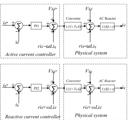
a. Inner current controller (Inner current loop)
The inner current controller is developed based upon equation (4.6). Figure 4.7 shows the d-axis and q-axis current controllers of the inner current loop.
The converter has a delay of e-Tws ≈1/(1+Tws) due to the sinusoidal pulse width modulator and Tw=1/2fs where fs is the switching frequency of the converter. Proportional integral (PI) controllers are used for closed loop control and the zeroes of the PI controllers are selected to cancel the dominant pole in the external circuit. For a typical VSC, the time constant τ=L/r is much higher than Tw and hence will be the dominant pole to be canceled.
The cross coupling currents in equation (4.6) are compensated by feed forward terms in the controllers as shown in Figure 4.7.
∑
+
-
PI1∑
+
+
+
1/(1+TwS)∑
-1/(SL+r) id* id rid-
ωLiq VXd* VXd idActive current controller Physical system
+
∑
+
-
PI2∑
+
+
+
1/(1+TwS)∑
-1/(SL+r) iq* iq rid+ωLid VXq* VXq rid+ωLid iqReactive current controller Physical system
+
Converter AC Reacter
Converter AC Reacter
rid
-
ωLiqFigure 4.7: Inner current controllers
b. Outer controllers
The outer controllers consist either of AC voltage and reactive power controllers and either of DC voltage or active power controllers. Active current (id) is used to control either of active power flow or DC voltage level. Similarly, the reactive current (iq) is used to control either of reactive power flow into stiff grid connection or AC voltage support in weak grid connection.
4.3.1 Active Power Control
The apparent active power flow is given by equation (4.13) and from equation (4.12);
Vxd =Vx (4.14)
Where Vx is resultant voltage in d-q reference frame and is desired to have constant value. Hence active power flow can be controlled by active current (id) and the active power controller is given by Figure 4.8.
∑
+
-
PI3P
refP
i
max-i
maxi
d*
Figure 4.9: PI controller for active power control
The output of the active power controller (id*) will be the reference input to the d-axis current controller of the inner current loop in Figure 4.7.
In order to limit the magnitude of current in the VSC HVDC to a maximum limit, the output of the active power controller is followed by a limiter function of +/-imax limits, where:
imax =irated (4.15)
4.3.2 Reactive Power Control
The reactive power from equation (4.13) is given by:
3 2
dq xd q
Q =− U i (4.16)
The reactive power is controlled by reactive current (iq*) and is implemented as in Figure 4.9.
∑
+
-
PI4 Qref Q iq-max -iq-max iq*Figure 4.9: PI controller for reactive power control
controller of the inner current loop in Figure 4.7.
iq* is limited to +/-Iq-max in such a way that the total converter current should not exceed the rated current (Imax=Irated). This takes the assumption that that priority is given to transfer of active power. Hence: 2 *2 _ q max max d i = I −i (4.17)
4.3.3 DC Voltage Control
From energy balance of the VSC-HVDC terminal:
0 3 0 2 ac DC cap xd d DC DC DC cap P P P V i V I V i + + = + + = (4.18)
where IDC and icap are the DC bus current and the capacitor current respectively. From equation (4.18) the current through the capacitor will be:
(3 2 Xd d cap DC DC V i i V = − +I ) (4.19)
And the same current in terms of voltage across the capacitor is given by:
DC cap dV i C dt = (4.20)
3 1 ( ) 2 3 2 ( ) 2 3 DC Xd d DC DC Xd d DC d D DC Xd dV V i I dt C V V i V i I CV V = − + − = + C (4.21)
From equation (4.21) it is seen that DC voltage can be regulated by control of active current (id*). The IDC term in equation (4.21) is compensated by feed forward control in the DC voltage regulator.
∑
+
-
PI5U
DCrefU
DCi
max-i
maxi
d*
∑
+
-2V
DC3V
xdI
DCFigure 4.10: DC voltage regulator
4.3.4 AC Voltage Control
Weak grid connection has significant line resistance and inductance, as shown in Figure 4.11 This creates considerable amount of voltage fluctuations with changing active power flow. Therefore if the AC network connected to the VSC-HVDC terminal is a weak grid, the AC voltage at PCC must be regulated by the converter.
By applying KVL across the line impedance;
Vlx−Vls =(rline+ jwLline)is (4.22) Where Vx is the reference voltage (has an angle of zero), rline+jωLline is the line impedance and is
is given by: * * s x x x S i V P jQ V P jQ V ⎛ ⎞ = ⎜ ⎟ ⎝ ⎠ ⎛ + ⎞ = ⎜ ⎝ ⎠ ⎛ − ⎞ = ⎜ ⎟ ⎝ ⎠ ⎟ (4.23)
Substituting equation (4.23) into (4.22);
l l l l ( ) ( ) ( ) ( x s line line s s line line x
line line line line
s x x V V r j L i P jQ V r j L V Pr Q L P L Qr V j V V ω ω ω ω = + + ⎛ − ⎞ = + + ⎜ ⎟ ⎝ ⎠ + − = + + ) (4.24)
The quadrature axis change in voltage due to active and reactive power has little effect on the resultant voltage magnitude Vx. Therefore, Vx is approximately;
l l line line x s x Pr Q L V V V ω ⎛ + ⎞ = + ⎜ ⎝ ⎠⎟ (4.25)
In equation (4.25) P is determined by the desired amount of active power flow. Hence, voltage Vx
can be maintained constant by reactive power compensation. This relation is mathematically given by:
line x x L V V Q ω Δ = Δ (4.26)
The block diagram of the AC voltage controller is given by:
∑
+
-
PI6V
x-ref∆
Q*
V
xFigure 4.12: AC voltage control by reactive power compensation
∆Q* is a reference input to the reactive power controller (Figure 4.9).
4.3.5 Frequency Control
The active AC system consists of synchronous generators with natural frequency droop characteristics with respect to power. They also implement frequency droop control which is useful for distributed compensation for power unbalance occurring at some point in the system [10]. The VSC-HVDC can also be set to contribute to the aggregate frequency droop characteristics of the entire AC system. The frequency droop control can be realized as shown in Figure 4.13 [10].
∑
+
-
PI3 Pref P imax -imax id*∑
-+
fref∑
-+
f KK in Figure 4.13 is called frequency bias factor and is assigned according to desired amount of contribution of the VSC-HVDC terminal for frequency control.
4.4 Control Loop Transfer Functions
In order to specify the parameters of the different PI controllers, the open loop transfer functions (TFs) of each control scheme must be determined. In order to do so, first the Laplace transformed equivalent of the physical systems must be identified. System transfer function is derived from the linearized differential equation of the respective state variable.
When seen from an outer control loop, the time delay in an inner loop is approximately the sum of all the delays in the inner loop.
4.4.1 TF of Inner Current Loop
After eliminating the feed forward elements from Figure 4.7, the corresponding open loop transfer function of the inner current loop is established as follows.
1 1 1 2 2 2 1 1 1 1 . . . 1 1 1 1 1 1 . 1 1 i p i w i p i w T S O L K T S T S r S T S K T s T S r S ⎛ + ⎞⎛ ⎞ ⎛ ⎞ = ⎜ ⎟⎜ ⎟ ⎜ ⎟ + ⎝ + τ ⎠ ⎝ ⎠⎝ ⎠ ⎛ + ⎞⎛ ⎞ ⎛ ⎞ = ⎜ ⎟⎜ ⎟ ⎜ ⎟ + ⎝ + τ ⎠ ⎝ ⎠⎝ ⎠ (4.27) Where τ=L/r
4.4.2 TF of DC Voltage Control Loop
The block diagram of the complete DC voltage control loop is shown in Figure 4.14.
∑
+
-
PI5 UDCref UDC imax -imax Current loop∑
+
-2VDC 3Vxd IDC 1/(1+TeqS) 3Vxd 2VCD
∑
+
+
IDC 1/(CS) UDCFigure 4.14: Closed loop control diagram of DC voltage regulator
Neglecting the constant disturbances, the open loop transfer function becomes;
5 5 5 1 1 . . . . 1 2 i p i eq DC T S V O L K T S T S V Cs ⎛ ⎞ ⎛ + ⎞ = ⎜ ⎟⎜⎜ + ⎟⎟ ⎝ ⎠⎝ ⎠ 3 xd 1 (4.28)
where Teq is the total time delay in the current control loop.
4.4.3 TF of Active / Reactive Power Control Loops
The control loop for active power is shown in Figure 4.15.∑
+
-
PI3P
refP
Current loop1/(1+T
eqS)
3V
xd2
P
Figure 4.15: Active power control loop
The open loop gain of active (and reactive) power control is given by:
3 3 3 4 4 4 1 1 3 . . . 1 2 1 1 3 . 1 2 i x p i eq i x p i eq T S V O L K T S T S T S V K T S T S ⎛ ⎞ ⎛ + ⎞ = ⎜ ⎟⎜⎜ + ⎟⎟ ⎝ ⎠⎝ ⎠ ⎛ ⎞ ⎛ + ⎞ ⎜ ⎟ ⎜ ⎟⎜ + ⎟ ⎝ ⎠⎝ ⎠ d d (4.29)
4.4.4 TF of AC Voltage Control Loop for Weak Grid Connection
The AC voltage control diagram for weak grid connection is shown in Figure 4.16.∑
+
-
PI6V
ac-refV
ac Reactive power control loop1 /(1+T
eq2S)
V
xω
L
∆
V
ac∆
Q
refFigure 4.16: Block diagram of closed loop AC voltage control loop
The corresponding open loop transfer function is given by:
6 6 6 2 1 1 . . . 1 i p i eq T S V O L K T S T S L xd ω ⎛ ⎞ ⎛ + ⎞ = ⎜ ⎟⎜⎜ + ⎟⎟ ⎝ ⎠⎝ ⎠ (4.30)
4.4.5 TF of AC Voltage Control Loop for Passive AC Network
AC voltage control loop for passive load connection is shown in Figure 4.17.∑
+
-
PI7 1/(1+TwS) 1/(SL+r)Vac*
V
acVac
Converter AC Reacter ZL/(ZL+jωL) Load voltage ratiom
Figure 4.17: Block diagram of AC voltage control loop for passive load
The transfer function of the physical system in Figure 4.17 can be derived as follows. At steady state, the AC voltage magnitude at PCC is given by voltage divide rule:
L x c L Z V V Z j Lω = + (4.31)

![Figure 2.7: Harmonic spectrum of optimized PWM [7]](https://thumb-us.123doks.com/thumbv2/123dok_us/10181280.2920557/25.918.234.689.105.379/figure-harmonic-spectrum-optimized-pwm.webp)
![Figure 2.10: Switching patterns for two-level and three-level VSCs respectively [7]](https://thumb-us.123doks.com/thumbv2/123dok_us/10181280.2920557/28.918.216.702.403.668/figure-switching-patterns-level-level-vscs-respectively.webp)