N A N O E X P R E S S
Open Access
Temperature dependence of electronic behaviors
in quantum dimension junctionless thin-film
transistor
Ya-Chi Cheng
1, Hung-Bin Chen
1,2, Ming-Hung Han
2, Nan-Heng Lu
1, Jun-Ji Su
1, Chi-Shen Shao
2and Yung-Chun Wu
1*Abstract
The high temperature dependence of junctionless (JL) gate-all-around (GAA) poly-Si thin-film transistors (TFTs) with 2-nm-thick nanosheet channel is compared with that of JL planar TFTs. The variation of SS with temperature for JL GAA TFTs is close to the theoretical value (0.2 mV/dec/K), owing to the oxidation process to form a 2-nm-thick channel. The bandgap of 1.35 eV in JL GAA TFTs by fitting experimental data exhibits the quantum confinement effect, indicating greater suppression of Ioffthan that in JL planar TFTs. The measured∂∂VTthof−1.34 mV/°C in JL GAA nanosheet TFTs has smaller temperature dependence than that of−5.01 mV/°C in JL planar TFTs.
Keywords:Junctionless; Nanowire; Thin-film transistor (TFTs); Gate-all-around (GAA); Quantum confinement effect
Background
The junctionless nanowire transistor (JNT), which con-tains a single doping species at the same level in its source, drain, and channel, has been recently investiga-ted [1-6]. The junctionless (JL) device is basically a gated resistor, in which the advantages of junctionless devices include (1) avoidance of the use of an ultra shal-low source/drain junction, which greatly simplifies the process flow; (2) low thermal budgets owing to implant activation anneal after gate stack formation is eliminated, and (3) the current transport is in the bulk of the conductor, which reduces the impact of imperfect semi-conductor/insulator interfaces. As is widely recognized, the temperature dependence of threshold voltage (Vth) is
a parameter when integrated circuits often operate at an elevated temperature owing to heat generation. This ef-fect, accompanied with the degradation of subthreshold swing (SS) with temperature, causes the fatal logic er-rors, leakage current, and excessive power dissipation. Despite a previous work that characterized JNTs at high temperatures [7], there is no information regarding the JL thin-film transistor (TFT) at a high temperature yet.
Hence, this letter presents a high-temperature operation of JL TFTs with a gate-all-around structure (GAA) for an ultra-thin channel. The JL TFT with a planar struc-ture functions as the control device. The drain current (Id), SS, off-leakage current (Ioff), and Vthare also
evalu-ated for fabricevalu-ated devices. The JL GAA TFTs with a small variation in temperature performances along with simple fabrication are highly promising for future system-on-panel (SOP) and system-on-chip (SOC) applications.
Methods
The process for producing 2-nm-thick poly-Si nanosheet channel was fabricated by initially growing a 400-nm-thick thermal silicon dioxide layer on 6-inch silicon wa-fers. Subsequently, a 40-nm-thick undoped amorphous silicon (a-Si) layer was deposited by low-pressure chem-ical vapor deposition (LPCVD) at 550°C. Then, the a-Si layer was solid-phase recrystallized (SPC) and formed large grain sizes as a channel layer at 600°C for 24 h in nitrogen ambient. The channel layer was implanted with 16-keV phosphorous ions at a dose of 1 × 1014cm−2, followed by furnace annealing at 600°C for 4 h. Subse-quently, we performed a wet trimming process with a dilute HF chemical solution at room temperature and
* Correspondence:[email protected]
1
Department of Engineering and System Science, National Tsing Hua University, Section 2 Kuang Fu Road, Hsinchu 30013, Taiwan Full list of author information is available at the end of the article
shrink down channel thickness to be around 28 nm. The active layers, serving as channel, were defined by e-beam lithography and then mesa-etched by time-controlled wet etching of the buried oxide to release the poly-Si bodies. Subsequently, a 13-nm-thick dry oxide, consuming around 13-nm-thick poly-Si on both side of channel to form 2-nm-thick channel, and 6-nm-thick nitride by LPCVD were deposited as the gate oxide layer. The 250-nm-thick in-situ doped n + poly-silicon was deposited as a gate electrode, and patterned by e-beam and reactive ion
etching. Finally, passivation layer and metallization was performed. The JL planar TFT serves as a control with single gate structure.
[image:2.595.59.538.89.361.2]Results and discussion
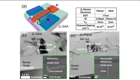
[image:2.595.59.540.552.704.2]Figure 1a presents the structure of the devices and rele-vant experimental parameters. Figure 1b displays the cross sectional transmission electron microscopic (TEM) images along the AA′direction in JL GAA devices with ten strips of nanosheet; the figure clearly shows that the Figure 1JL GAA device structure in JL TFTs and TEM images for JL GAA and JL planar. (a)The JL GAA device structure and relevant parameters in JL TFTs. The positions A and A′indicate cross section of channel.(b,c)The TEM images along AA′direction for JL GAA and JL planar with 2- and 15-nm channel thickness, respectively.
Figure 2Temperature dependence (25°C to 200°C) onId–Vgcharacteristics atVd= 0.5 V.For JL GAA TFTs (Lg= 1μm(b), 60 nm(c)) and
2-nm-thick nanosheet channel is surrounded by the gate electrode. The dimensions of each nanosheet are 2-nm high × 70-nm wide. Figure 1c displays the TEM images in JL planar devices, and the channel dimensions are 15-nm high × 0.95-μm wide. Figure 2 shows the mea-suredIdas a function of gate bias (Vg) at various
temper-atures ranging from 25°C to 200°C atVd= 0.5 V for (a)
JL planar TFTs with channel length (Lg) of 1μm, (b) JL
GAA TFTs with Lg= 1 μm, and (c) JL GAA TFTs with
Lg= 60 nm. This figure reveals that Vth decreases and
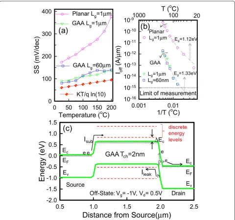
the SS increases in all devices when increasing the temperature. Figure 3 presents the measured SS and Ioff
as a function of temperature at Vd= 0.5 V, as extracted
from the Id-Vg curves in Figure 2. In Figure 3a, the JL
GAA TFTs have a small SS variation with temperature than JL planar TFTs. Furthermore, the SS can be ex-pressed as follows [8]:
SS¼ kTq ln10 1þq2tSiNT
Cox
; ð1Þ
where kT is the thermal energy, Cox is the gate oxide
capacitance per unit area,NTis the trap states, andtSiis
the thickness of the poly-Si layer. Therefore, the decline in SS of JL GAA TFTs is due to a decreasing tSi and the
formation of a crystal-like channel by oxidation. The
Temperature (
oC)
0
50
100 150 200
SS (
m
V/dec)
0
100
200
300
400
GAA L
g=1
μ
m
Planar L
g=1
μ
m
GAA L
g=60
μ
m
KT/q ln(10)
1/T (
oC)
0.001
0.01
I
off(A/
μ
m)
10
-1610
-1510
-1410
-1310
-1210
-1110
-1010
-91000
100
Limit of measurement
T (
oC)
20
GAA
Lg=60nm Lg=1μm
Planar
Lg=1μm Eg=1.12eV
Eg=1.33eV
Distance from Source(
μ
m)
0.5
1.0
1.5
2.0
2.5
En
ergy
(eV)
-2.0
-1.5
-1.0
-0.5
0.0
0.5
1.0
1.5
Off-State: V
g= -1V, V
d= 0.5V
I
sub(a)
(b)
(c)
e
e
h
I
leakdiscrete energy levels
Δ
E
cGAA T
ch=2nm
Source
Drain
E
FE
vE
c eeE
F [image:3.595.58.539.257.705.2]E
vE
cFigure 3Measured SS andIoffas function of temperature (a,b) and simulated band diagram of GAA structure (c). (a,b)AtVd= 0.5 V,
variation of the SS with temperature ∂SS
∂T for JL GAA TFTs is 0.25 mV/dec/K, which is slightly larger than the theoretical value of 0.2 mV/dec/K. The results represent the second term of Equation 1 is small and insensitive to temperature. According to Figure 3b, Ioff is defined as
the drain current at Vg=−1.9 V for JL planar TFTs and
at Vg=−0.2 V for JL GAA TFTs, respectively. Moreover,
Ioffcan be expressed as follows [9]:
Ioff¼IsubþIleak∝ exp −
qEg
2kT
; ð2Þ
whereIsubis the subthreshold current,Ileakis the
trap-induced leakage current, andEg is the bandgap. TheEg
could be regarded as a constant value for estimation, be-cause ∂∂ETg is known to be −0.27 meV/K [10]. Therefore, the Eg of JL planar and GAA TFTs, as extracted by
Equation 2, is around 1.12 and 1.35 eV, respectively. Not-ably, quantum confinement is observed in JL GAA TFTs, resulting in band-edge shifts (ΔEc) of the
conduction-band and valence-conduction-band, thereby increasing the Eg to
re-duce the off-state leakage current, as shown in Figure 3c. Figure 3c illustrates the band diagram of the GAA device in off-state with discrete energy levels. The GAA device is simulated by solving 3D quantum-corrected device simu-lation using the commercial tool, Synopsys Sentaurus De-vice [11, 12] to obtain accurate numerical results for a nanometer-scale device. These simulation performances are calibrated to experimental data ofId–Vg. TheΔEcis
estimated around 0.23 eV, as extracted from the experi-mental data in Figure 3b. The theoretical analysis derived
from the solution of the Schrödinger equation for the first level in the conduction band as follows [10]:
ΔVth¼Δ
Ec
q ¼
h2
8qme 1
T2
ch
þW12
; ð3Þ
where me* is the electron effective mass, h is Plank's
constant,Tchis the channel thickness andWis the
chan-nel width. The second term in Equation 3, which repre-sents quantum confinement effect in the channel width direction, can be ignored due toW > >Tch. TheΔVthof
theoretical value is 0.36 eV, which is larger than experi-mental value of 0.23 eV. The gap would come from the poly-Si channel material.
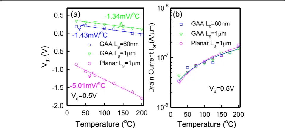
Figure 4a presents the measured Vthas a function of
temperature. The Vth is defined as the gate voltage at
Id= 10−9A. The temperature coefficients ofVthare−1.34
and −5.01 mV/°C for GAA and planar JL TFTs, respect-ively. According to [13], the variation of ∂Vth
∂T in n-type JL devices can be expressed as follows [13]:
∂Vth
∂T ¼
∂Vfb
∂T ‐ q
εSi
A P
2
þCqA
ox
" #
∂ND
∂T þ
1
q
∂ΔEc
∂T ; ð4Þ
where Vfb is the flat-band voltage, Cox is the gate
oxide capacitance per unit length, Ais the device cross-sectional area and Pis the gate perimeter. The first term in the right side of Equation 4 is depended on the flat-band voltage variation with temperature. For ND= 1 ×
1019cm−3, the value of∂Vfb
[image:4.595.58.537.488.704.2]∂T is approach to−0.49 mV/°C as the devices in [13], which has a P+ polycrystalline silicon gate and the same doping concentration. The second term
Figure 4Impact of temperature dependence on the (a)Vthand (b) on-state currents.For JL GAA TFTs (Lg= 1μm, 60 nm) and JL planar
represents the effect of incomplete ionization. The doped impurities are almost completely ionized at those temper-atures higher than room temperature. Thus, the doping concentration variation with the temperature ∂ND
∂T
has a slight dependence on temperature. The third term, de-pending on the electron effective mass, also has a smaller dependence on T than the other terms. The theoretical value of ∂Vth
∂T is about −0.49 mV/°C; although the ∂∂VTth of−1.34 mV/°C in JL GAA TFTs is larger than theoretical value, but is comparable with current SOI-based JNT (∂Vth ∂T approximately −1.63 mV/°C) [7] due to the use of the multi-gate structure and formation of a crystal-like na-nosheet channel with fewer traps by oxidation process. Therefore, JL TFTs with the GAA structure and ultra-thin channel shows an excellent immunity to the temperature dependence on Vth and competes with SOI-based JNT.
Figure 4b presents the measured on-current (Ion) as a
function of temperature. The Ion is defined as the drain
current atVg= 3 V for JL planar TFTs and atVg= 6 V for
JL GAA TFTs. The JL GAA TFTs show a slightly better
Ionvariation with temperature than the planar ones,
pos-sibly owing to a smaller∂Vth
∂T in JL GAA TFTs.
Conclusion
This work has presented a high-temperature operation of JL TFTs. The high temperature dependence of JL GAA and planar TFTs is also studied. The variation of parameters such as Vth, Ion, SS, and Ioff are analyzed as
well. The variation of the SS with temperature for JL GAA TFTs is close to the ideal value (0.2 mV/dec/K) owing to the ability of the oxidation process to form a nanosheet channel and crystal-like channel. Additionally,
Ioff is negligibly small for JL GAA TFTs, owing to
quantum confinement effect; itsEgof 1.35 eV is also
ex-tracted. The JL GAA TFTs have a smaller ∂Vth
∂T than that of JL planar TFTs owing to the GAA structure and ultra-thin channel. Moreover, the measured ∂Vth
∂T of JL GAA TFTs competes with that of SOI-based JNTs. Therefore, the JL GAA TFTs with a slight variation in tempera-ture performances along with simple fabrication are highly promising for future SOP and system-on-chip SOC applications.
Competing interests
The authors declare that they have no competing interests.
Authors’contributions
YCC and HB handled the experiment and drafted the manuscript. MH made the simulation plot and performed the electrical analysis. NH, JJ, and CS fabricated the samples and carried out the electrical characterization. YCW supervised the work and reviewed the manuscript. All authors read and approved the final manuscript.
Acknowledgements
The authors would like to acknowledge the National Science Council of Taiwan for supporting this research under Contract No. MOST
103-2221-E-007 -114 -MY3. The National Nano Device Laboratories is greatly appreciated for its technical support.
Author details
1Department of Engineering and System Science, National Tsing Hua
University, Section 2 Kuang Fu Road, Hsinchu 30013, Taiwan.2Department of Electronics Engineering & Institute of Electronics, National Chiao Tung University, 1001, Ta Hsueh Road, Hsinchu 30013, Taiwan.
Received: 8 April 2014 Accepted: 9 July 2014 Published: 13 August 2014
References
1. Lee CW, Afzalian A, Akhavan ND, Yan R, Ferain I, Colinge JP:Junctionless multigate field-effect transistor.Appl Phys Lett2009,94:053511. 2. Colinge JP, Lee CW, Afzalian A, Akhavan ND, Yan R, Ferain I, Razavi P,
O’Neil B, Blake A, White M, Kelleher AM, McCarthy B, Murphy R:Nanowire transistors without junctions.Nat Nanotechnol2010,5:225.
3. Colinge JP, Lee CW, Ferain I, Akhavan ND, Yan R, Razavi P, Yu R, Nazarov AN, Doria RT:Reduced electric field in junctionless transistors.Appl Phys Lett
2010,96:073510.
4. Lin HD, Lin CI, Huang TY:Characteristics of n-Type Junctionless Poly-Si Thin-Film Transistors With an Ultrathin Channel.IEEE Electron Device Lett
2012,33:53.
5. Su CJ, Tsai TI, Liou YL, Lin ZM, Lin HC, Chao TS:Gate-all-around junctionless transistors with heavily doped polysilicon nanowire channels.IEEE Electron Device Lett2011,32:521.
6. Rios R, Cappellani A, Armstrong M, Budrevich A, Gomez H, Pai R, Rahhal-orabi N, Kuhn K:Comparison of Junctionless and conventional trigate transistors with Lg down to 26 nm.IEEE Electron Device Lett
2011,32:1170.
7. Lee CW, Borne A, Ferain I, Afzalian A, Yan R, Akhavan ND, Razavi P, Colinge JP:High-temperature performance of silicon junctionless MOSFETs.
IEEE Electron Device2010,57:620.
8. Dimitriadis CA:Gate bias instability in hydrogenated polycrystalline silicon thin film transistors.J Appl Phys2000,88:3624.
9. Guo X, Ishii T, Silva SRP:Improving switching performance of thin-film transistors in disordered silicon.IEEE Electron Device Lett2008,29:588. 10. Sze SM, Ng K:Physics of Semiconductor Devices.3rd edition. New York: Wiley;
2007.
11. Synopsys, Inc:Sentaurus Device User Guide.Mountain View: Version I-2013.12; 2013.
12. Ancona MG, Iafrate GJ:Quantum correction to the equation of state of an electron gas in a semiconductor.Phys Rev B1989,39:9536.
13. Trevisoli RD, Doria RT, de Souza M, Pavanello MA:Threshold voltage in junctionless nanowire transistors.Semiconductor Sci Technol2011,26:1.
doi:10.1186/1556-276X-9-392
Cite this article as:Chenget al.:Temperature dependence of electronic behaviors in quantum dimension junctionless thin-film transistor.
Nanoscale Research Letters20149:392.
Submit your manuscript to a
journal and benefi t from:
7Convenient online submission
7Rigorous peer review
7Immediate publication on acceptance
7Open access: articles freely available online
7High visibility within the fi eld
7Retaining the copyright to your article