N A N O E X P R E S S
Open Access
Smooth ZnO:Al-AgNWs Composite
Electrode for Flexible Organic
Light-Emitting Device
Hu Wang
1,2, Kun Li
1,2, Ye Tao
2, Jun Li
2, Ye Li
1, Lan-Lan Gao
1*, Guang-Yong Jin
1and Yu Duan
1,2*Abstract
The high interest in organic light-emitting device (OLED) technology is largely due to their flexibility. Up to now, indium tin oxide (ITO) films have been widely used as transparent conductive electrodes (TCE) in organic opto-electronic devices. However, ITO films, typically deposited on glass are brittle and they make it difficult to produce flexible devices, restricting their use for flexible devices. In this study, we report on a nano-composite TCE, which is made of a silver nanowire (AgNW) network, combined with aluminum-doped zinc oxide (ZnO:Al, AZO) by atomic layer deposition. The AgNWs/AZO composite electrode on photopolymer substrate shows a low sheet resistance of only 8.6Ω/sq and a high optical transmittance of about 83% at 550 nm. These values are even comparable to conventional ITO on glass. In addition, the electrodes also have a very smooth surface (0.31 nm root-mean-square roughness), which is flat enough to contact the OLED stack. Flexible OLED were built with AgNWs/AZO electrodes, which suggests that this approach can replace conventional ITO TCEs in organic electronic devices in the future.
Keywords:Silver nanowires, Al-doped ZnO, Atomic layer deposition, Transparent conductive electrode, Organic light-emitting device
Background
Transparent conducting electrodes (TCEs) have been widely used in photo-electronic devices such as thin film transistors, thin film solar cells, and organic light-emitting devices (OLEDs) [1–3], due to their excellent optical and electrical properties, in particular, indium tin oxide (ITO) [4]. However, ITO has important disadvan-tages. It is increasingly expensive and hard to produce in a sustainable manner because of a limited supply of indium. In addition, its fragility is a mismatch with the demands by flexible electronics, the next generation light source, and display technology [5–7]. Recently, a variety of materials have been investigated as substitutes for ITO, including conjugated polymers [8], carbon nano-tubes (CNTs) [9], graphene [10], silver nanowires (AgNWs) [11, 12], and metal oxides such as zinc oxide (ZnO) [13, 14]. Among these alternatives, AgNWs, which uses one-dimensional nano-sized silver as the
primary material, are most promising because of their outstanding electrical, optical and mechanical properties, Furthermore, AgNWs films can be deposited using a low-cost solution process, Dong-Seok Leem et al. [15] fabricated P3HT:PCBM OSCs using AgNWs as the lower electrode, leading to high PCEs of up to 3.5%. Nonetheless, pure AgNWs films have several drawbacks, such as a high surface roughness, a large junction resist-ance, and a small contact area [16, 17]. The buried-layer structure, which comprises a AgNWs film and a metal− oxide layer, has been suggested as an alternative to over-come these issues [18–20]. Sanggil Nam et al.[21] had reported that AgNWs electrode embedded in NOA63 has an ultra-smooth surface with a root-mean-square (RMS) of 0.4 nm and Rpv of 4.557 nm.
In our previous work, we have prepared AgNWs/ZnO electrode in which ZnO as a conductive-bridging for AgNWs was deposited by low temperature (60 °C) ALD [22], but the sheet resistance was higher than AgNWs. In this work, we reported an AgNWs/AZO hybrid film on a photopolymer NOA63 substrate, where AZO was deposited 6 nm by ALD. AZO reduced the junction * Correspondence:[email protected];[email protected]
1College of Science, Changchun University of Science and Technology,
Changchun 130012, China
Full list of author information is available at the end of the article
resistance immensely by strengthening the junction con-nection of the AgNWs. It also increased the contact area by filling open spaces between the AgNWs. Macroscop-ically, AZO reduced the sheet resistance of the AgNWs film. It cut down the height difference between the AgNWs and the substrate, and smoothed out the surface roughness. A composited TCE with a low sheet resist-ance of 8.6Ω/sq, a transmittance of 83% at 550 nm, and less than 1 nm surface roughness was obtained.
Methods
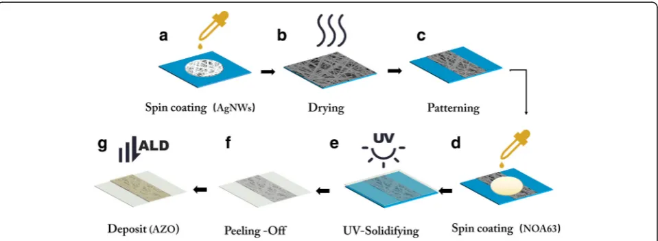
The procedures to fabricate the electrodes are shown in Fig. 1. Isopropanol-based solutions of AgNWs (XFNano Company, NanJing, China) with a ratio of length to diameter (70 nm × 100μm) were shaken in an ultrasonic machine for 5 min and deposited on a clean silicon sub-strate via spin coating at 6000 rpm for 30 s. We chose the large length diameter ratio of silver nanowires. This was because at the same concentration the longer nano-wires form films with better conductivity and a better surface topography. Then, the AgNWs film was dried in an oven at 150 °C for 10 min in order to remove solvent and to soften the AgNWs, followed by the“Patterning”, which means wiping off the AgNWs on both sides of silicon. An alcohol cotton ball was used to wipe off AgNWs and only leave the middle part (1 cm wide). Because the anode and cathode of our organic light-emitting device are crossed, they will be connected dir-ectly if we did not wipe off AgNWs on both sides. After patterning, NOA63 (Norland Optics, Norland Products, Cranbury, NJ, USA), a type of photoresist, was deposited on the AgNWs film by spin coating with 300 rpm for 15 s first, and then 600 rpm for 15 s. The samples were exposed to ultraviolet light at a 300–370-nm wavelength
for 4 min for solidifying, and a flexible AgNWs-only electrode was obtained.
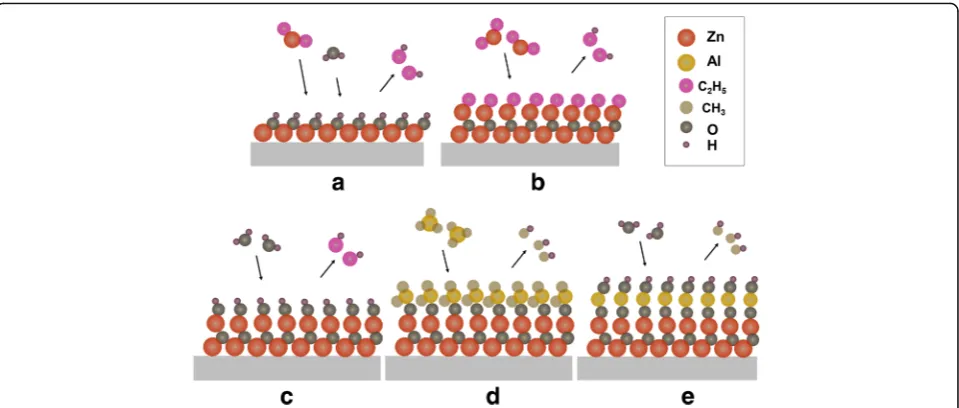
The AZO was grown with a Lab Nano 9100 ALD system (Ensure Nanotech Inc. Beijing, China) at 150 °C which could soften the AgNWs and made them intercon-nect better, and this temperature has little effect on the NOA63 and the electrode. The equation shown in Fig. 2 indicates that diethyl zinc ((C2H5)2Zn, DEZ) and tri-methyl aluminum (Al(CH3)3, TMA), re-spectively, react with H2O in the reaction chamber with a constant 20 sccm flow of high purity N2, which carries and purges the residual precursor va-pors at 0.1 Torr pressure. High purity nitrogen was used as the purging gas; the purging time was long enough to exhaust gaseous residual products, includ-ing gaseous precursors without reactions and gas-eous reaction products. So, there are almost no residual products in ALD process. As shown in Fig. 2a, DEZ and H2O react on the substrate surface, and –C2H5 react with H2O and generate one layer of –OH functional groups on the top of the sedi-mentary layer. Then, to access the DEZ, as shown in Fig. 2b, one of the –C2H5 on DEZ react with –OH and generate C2H6; this process is performed accord-ing to Eq. (1). For the next reaction, shown in Fig. 2c considering to Eq. (2), to access H2O, the –C2H5 react with H2O and generate –OH functional groups on the top of the sedimentary layer. This is the same for the process in Fig. 2a. Equations (1) and (2) rep-resent a reaction cycle, and then ZnO is grown layer by layer. The principle of growing Al2O3 is similar to ZnO, to access TMA, −CH3 on TMA react with –OH and generate CH4, then to access H2O, react with –CH3, and completes doping of Al—see Fig. 2d, (e) and Eqs. (3) and (4) [23].
Fig. 1The flow-process of fabricating flexible electrode.aDropping AgNWs solution and spin coating.bDrying in the oven at 150 °C.cPatterning electrode.dDropping NOA63 and spin coating.eExposing under ultraviolet light with 300–370 nm wavelength for 4 min.fPeeling the NOA63 off.
gDepositing AZO by ALD
[image:2.595.59.539.519.695.2]Surf−ZnðOHÞ þZnðCH2CH3Þ2→Surf−ZnOZnðCH2CH3Þ þC2H6
ð1Þ
Surf′−ZnðCH2CH3Þ þH2O→Surf′−ZnðOHÞ þC2H6 ð2Þ
Surf′−ZnðOHÞ þAlðCH3Þ3→Surf′−ZnOAlðCH3Þ2þCH4 ð3Þ
Surf″−AlðCH3Þ þH2O→Surf″−AlðOHÞ þCH4 ð4Þ
ZnO is accessed with the 0.03 s pulses, and after waiting 30 s, H2O is accessed to oxidize DEZ. Then it takes 100 s to purge completely both the C2H6and the residual gas. The growing of Al2O3 follows a cycle sequence: 0.02 s TMA dose, 30 s waiting, 0.02 s H2O dose, 100 s purge. According to the parameters above, we deposited 3 nm AZO as follows: 15 cycles ZnO/1 cycle Al2O3/15 cycles ZnO, and 6 nm of 20 cycles ZnO/1 cycle Al2O3/20 cycles ZnO/1 cycle Al2O3/20 cycles ZnO, and 9 nm of 22 cy-cles ZnO/1 cycle Al2O3/22 cycles ZnO/1 cycle Al2O3/ 22 cycles ZnO/1 cycle Al2O3/22 cycles ZnO. The doping ratio of Al was optimized at 3 at.% for all depositions.
Finally, we fabricated green light OLEDs with the AgNWs/AZO composite anode. The structure of the OLED was 2 nm MoO3grown on anode as a hole-buffer layer; 30 nm thick 4,4′,4″-tris (N-3-methylphenyl-N-phenylamino)-triphenylamine (m-MTDATA) as hole-injection layer; 20 nm thick N,N’-biphenyl N,N’-bis (1-naphenyl)-[1,1′-biphenyl]-4,4′-diamine (NPB) as a hole transport layer; 30 nm thick tris-(8-hydroxyquinoline) aluminum (Alq3) doped with 1% 10-(2-benzothiazolyl)- 2,3,6,7-tetrahydro-1,1,7,7-tetramethyl-1H,5H,11H-(1)-benzopyropyrano(6,7-8-I,j) quinolizin-11-one (C545T) as the main light-emitting layer; 20 nm of Alq3 as the
electron transport layer; 0.5 nm of Liq and 100 nm Al as the cathode. The active area is 0.1 cm2. An Agilent B2902A source meter and a Minolta lumi-nance meter LS-110 were used to measure the current density–voltage–luminance (I–V–L) character-istics of the flexible devices.
Results and Discussions
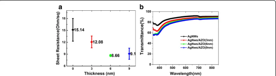
In order to compare the optical and electrical properties, we fabricated samples of AgNWs electrodes with differ-ent thicknesses of AZO, and we prepared an AgNWs-only sample for reference. Figure 3a shows the effect for composite electrodes with different thicknesses of AZO layers on the sheet resistance. The AgNWs-only film had floating values on for Rs from 12.7 to 18.0 Ω/sq because the rough surface of the electrode produces ran-dom connection with the four-point probe. The sample with 3, 6, and 9 nm AZO had 12.0 ± 1.5, 8.66 ± 0.4, and 9.1 ± 1.4Ω/sq, respectively [24]. For organic device elec-trodes, the optical transmittance is an important param-eter, because it directly affects the light output coupling. Figure 3b shows transmittances of different electrode grown with 0, 3, 6, 9 nm thickness AZO in the range of visible light wavelength. At 550 nm, the transmittance of the AgNWs-only electrode was 89%. In this work, the transmittance depended on both the concentration of AgNWs solution and the spin-coating speed. Here, we selected a 5 mg/ml concentration and 6000 rmp speed considering to our previous research [22]. The transmit-tance of the electrode for 3 nm AZO was 85% at 550 nm wavelength, for 6 nm AZO it was 83%, and for 9 nm AZO it was 81%. With the increase of the thick-ness of AZO, the transmittance decreased. For the
Fig. 2The schematics of the reaction process in ALD.aReaction DEZ and H2O reacting.bAccessing DEZ, reacting and discharging C2H6.cAccessing
[image:3.595.59.539.87.291.2]electrode, both the excellent conductivity and optical transmittance are necessary; however, the two properties usually mutually restrict; a thicker film tends to have a better conductivity but lower transmittance. In order to optimize the trade-off between transmittance and sheet resistance, the following figure of merit (ΦFM) [25], as defined by Haacke, was introduced into our work:
ΦFM¼T 10
RS ;
whereTis the transmittance at a wavelength of 550 nm
and Rs is the sheet resistance (Ω/sq). The ΦFM values
calculated by this formula are expected to be better the bigger they are. Here, we chose the four-test point
method for each sample and calculate ΦFM. In Table 1,
theΦFMof the three different samples was summarized.
ΦFM of AgNWs electrode with 3 nm AZO was 16.406,
with 6 nm it was 17.917 which is the highest value and with 9 nm it was 13.360. Although 3 nm AZO affected on transmittance less than thicker AZO, it had poor connectivity for AgNWs on substrate surface. This was not as good as the 6 and the 9 nm AZO layer. The rea-sons are that 3 nm was too thin to form a continuous AZO layer, so the reduction of Rs was limited. For the 9 nm AZO modified layer, we obtained a relatively low
Rs of 9.1 Ω/sq; however, the AZO film has a low
trans-mittance compared to the AgNWs-only electrode. If AZO is grown thicker, the Rs reduction of the composite electrode will slow down because AZO as a semiconductor
material itself is lacking carriers. The Rs was higher than for the AgNWs film according to the report by Manuela Göbelt, where the pure AZO film has an 18
times higher Rs (368 Ω/sq) than the heated AgNWs
network [26], while its transmittance will decrease.
Therefore, we optimized the thickness of the modified AZO layer of 6 nm. It was not only perfectly con-nected AgNWs on the surface of substrate and decreased sheet resistance of AgNWs film, but also had up to 83% light transmittance.
Furthermore, the AZO modified layer also contributed to the improved surface smoothness. Figure 4 shows the image taken with atomic force microscope (AFM) in tapping mode, including a three-dimensional diagram, planar diagram, and the height line profiles of the AgNWs on a silicon chip, as well as AgNWs embedded in NOA63, and AgNWs embedded NOA63 covered with AZO. The roughness of the directly prepared AgNWs on the silicon substrate is very high, and the maximum can reach several hundred nanometers. A RMS of 58.83 ± 0.05 nm and a maximum peak-to-valley (Rpv) of 276.46 ± 0.05 nm were measured. It was easy to cause short circuits in the devices because the total thickness of the organic layers of the devices is below 100 nm. The AgNWs em-bedded in the NOA63 film showed a surface with RMS of 0.37 ± 0.02 nm and Rpv of 5.28 ± 0.03 nm. This shows clearly that the NOA63 not only fills the open spaces, but also covers the protruding thorns and crossing knots of AgNWs. The use of NOA63 is a common method, but after peeling NOA63 off, the surface of electrode is not smooth enough. After the fabrication of the device, the first layer of MoO3was only 2 nm thick, so the roughness of surface of electrode must decrease. In this work, we introduced an AZO layer and measured the sur-face roughness of the AgNWs embedded NOA63 with AZO. The obtained RMS is 0.31 ± 0.01 nm, while the Rpv is 4.87 ± 0.02 nm. Both values are lower than the values for AgNWs embedded NOA63. This indicates the modified AZO layer also contributes significantly
[image:4.595.59.539.88.220.2]Fig. 3aThe averages and error values of sheet resistance of AgNWs-only and AgNWs with 3, 6, and 9 nm AZO electrodes.bThe transmittance of AgNWs-only and AgNWs with 3, 6, and 9 nm AZO electrodes in visible light range
Table 1Characteristic values of for all samples with different thicknesses for the AZO modified layer
Structure Thickness of AZO (nm)
Average of Rs (Ω/sq)
Transmittance at 550 nm
Figure of merit (ΦFM× 10−3)
AgNWs/AZO 3 12.0 85% 16.406
AgNWs/AZO 6 8.6 83% 17.917
AgNWs/AZO 9 9.1 81% 13.360
[image:4.595.56.291.665.733.2]to the improved surface smoothness [18, 27]. It also suggests the surface of the AgNWs electrode was not smooth enough alter peel off; the reasons may be at-tributed to the viscosity of NOA63. When NOA63 flows into the vacancy of the AgNWs, the high vis-cosity prevented NOA63 from permeating through and bonding with the AgNWs. Therefore, gaps be-tween AgNWs and NOA63 substrate are present on
nanoscale, see Fig. 4b. The AZO film improved the surface roughness further by filling these gaps. It thus created a smoother surface for the organic layer [28]. As we can see in Fig. 4c, a homogeneous surface was obtained by depositing the AZO film on AgNWs em-bedded on the NOA63 substrate.
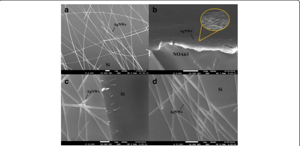
Figure 5a shows the SEM image of AgNWs on a sili-con substrate. As we know, the photoelectric properties
Fig. 4Three-dimensional AFM images in tapping mode, planar diagram and height line profiles of three samplesa. The AgNWs spin-coated on a silicon chip.bAgNWs embedded in NOA63.cAgNWs/AZO (6 nm) embedded NOA63 (5 × 5 um)
[image:5.595.59.539.87.305.2] [image:5.595.58.539.480.714.2]of AgNWs-based transparent electrodes depend on the density of meshwork. With increasing density, the con-ductivity increases due to the better connection between AgNWs, while transmittance decreases because of the reflection of AgNWs mesh. AgNWs with a large length to diameter ratio can effectively ensure high electrical conductivity, but it also reduces the reflection to balance its light transmittance. The plane graph of AgNWs em-bedded in NOA63 is shown in Fig. 5b. The AgNWs be-comes blurred in enlarged view, which suggests that AgNWs was embedded in NOA63. This was also in ac-cordance with the AFM result shown in Fig. 4b. Figure 5c and d presents a profile and plane photograph of the AgNWs/AZO composite electrode on a silicon sub-strate, the shadows on the AgNWs reveal an AZO film with a thickness of 6 nm blanketed AgNWs that form a core-shell structure and enhanced between the AgNWs [26].
Figure 6 shows I–V–L characteristic of the green or-ganic light-emitting device with the composite AgNWs/AZO electrode and AgNWs-only electrode. The thickness of AZO was 6 nm. It was observed that the green OLED with the AgNWs/AZO compos-ite electrode produces a higher current density than the AgNWs-only reference electrode when the voltage exceeded 9 V, see Fig. 6a. This illustrates that the AZO layer enhanced hole-injection of the AgNWs layer improved the carrier recombination. Figure 6b shows the luminance–voltage characteristics for the two electrodes; the maximum luminance of composite electrode was up to 10,000 cd/m2
at 14 V, which was brighter than for the OLED with AgNWs electrode under same voltage. However, the turn-on-voltage, which is defined as the required voltage to obtain 1 cd/m2 of light output, was higher than for the AgNWs electrode see Fig. 6b. The reason of this may be the work function of our composite electrode, which causes a bit slightly higher barrier for hole-junction at low current density.
Conclusions
We have demonstrated that AZO as a modified layer can improve both connectivity and surface roughness in flexible AgNWs electrodes. The best thickness of the AZO modified layer was 6 nm according to our experi-ments. The optimized AgNWs/AZO composite elec-trode shows a high transmittance of 83% and a low sheet resistance of 8.6Ω/sq, as well as a smooth surface of 0.31 nm root-mean-square roughness. These are com-parable to conventional ITO films. The green organic light-emitting device fabricated, using AgNWs/AZO as transparent conducting electrode, has a better I–V–L characteristic than the AgNWs-only device. These re-sults suggest that the smooth AgNWs/AZO composite electrode can be used for flexible organic light-emitting devices and other flexible devices without loss of optical and electrical performance.
Abbreviations
AgNWs:Silver nanowires; DEZ: [Zn(C2H5)2]: Diethylzinc; ITO: Indium tin oxide; TMA: Trimethylaluminium
Acknowledgements
This study was supported by the International Science and Technology Cooperation Program of China (2014DFG12390), the National High Technology Research and Development Program of China (Grant No. 2011AA03A110), National key research program of China (Grant No. 2016YFB0401001), the National Natural Science Foundation of China (Grant Nos.61675088, 61275024, 61377026, 61274002, and 61275033), the Scientific and Technological Developing Scheme of Jilin Province (Grant No. 20140101204JC, 20130206020GX, 20140520071JH, 20130102009JC), the Scientific and Technological Developing Scheme of Changchun (Grant No. 13GH02), and the Opened Fund of the State Key Laboratory on Integrated Optoelectronics No. IOSKL2012KF01. Prof. Duan wants to thank Dr. M. Mazeeo and Prof. G. Gigli from NNL in Lecce, Italy, for useful discussion.
Authors’contributions
HW and KL carried out the design of the study and drafted this manuscript. YD, LLG, and GYJ conceived of the study and participated in its design and coordination. YT, YL, and JL carried out the preparation of the samples and characteristic measurements. All authors read and approved the final manuscript.
Competing interests
The authors declare that they have no competing interests.
Fig. 6I–V–L characteristic of the green light-emitting device.aCurrent density–voltage characteristics of the AgNWs/AZO (6 nm) composite electrode and the referential AgNWs-only electrode.bLuminance–voltage characteristics of the AgNWs/AZO(6 nm) composite electrode and the AgNWs-only reference electrode
[image:6.595.59.539.88.216.2]Author details
1College of Science, Changchun University of Science and Technology,
Changchun 130012, China.2State Key Laboratory on Integrated
Optoelectronics, College of Electronic Science and Engineering, Jilin University, Jilin 130012, China.
Received: 18 December 2016 Accepted: 8 January 2017
References
1. Xia YJ, Sun K, Ouyang JY (2012) Solution-processed metallic conducting polymer films as transparent electrode of optoelectronic devices. Adv Mater 24(18):2436–2440
2. Hecht DS, Hu LB, Irvin G (2011) Emerging transparent electrodes based on thin films of carbon nanotubes, graphene, and metallic nanostructures. Adv Mater 23(13):1482–1513
3. Fortunato E, Ginley D, Hosono H, Paine DC (2007) Transparent conducting oxides for photovoltaics. MRS Bull 32(3):242–247
4. Helander MG, Wang ZB, Qiu J, Greiner MT, Puzzo DP, Liu ZW, Lu ZH (2011) Chlorinated indium Tin oxide electrodes with high work function for organic device compatibility. Science 332(6032):944–947
5. Cheong HG, Triambulo RE, Lee GH, Yi IS, Park JW (2014) Silver nanowire network transparent electrodes with highly enhanced flexibility by welding for application in flexible organic light-emitting diodes. ACS Appl Mater Interfaces 6(10):7846–7855
6. Wu JB, Agrawal M, Becerril HA, Bao ZN, Liu ZF, Chen YS, Peumans P (2010) Organic light-emitting diodes on solution-processed graphene transparent electrodes. ACS Nano 4(1):43–48
7. Morales-Masis M, Dauzou F, Jeangros Q, Dabirian A, Lifka H, Gierth R, Ruske M, Moet D, Hessler-Wyser A, Ballif C (2016) An indium-free anode for large-area flexible OLEDs: defect-free transparent conductive zinc tin oxide. Adv Funct Mater 26(3):384–392
8. Benor A, Takizawa SY, Perez-Bolivar C, Anzenbacher P (2010) Efficiency improvement of fluorescent OLEDs by tuning the working function of PEDOT:PSS using UV-ozone exposure. Org Electron 11(5):938–945 9. Chien YM, Lefevre F, Shih I, Izquierdo R (2010) A solution processed top
emission OLED with transparent carbon nanotube electrodes. Nanotechnology 21(13).
10. Han TH, Lee Y, Choi MR, Woo SH, Bae SH, Hong BH, Ahn JH, Lee TW (2012) Extremely efficient flexible organic light-emitting diodes with modified graphene anode. Nat Photonics 6(2):105–110
11. Cui HF, Zhang YF, Li CN (2014) Flexible organic light-emitting devices with a smooth and transparent silver nanowire electrode. Optical Engineering 53(7). 12. Tokuno T, Nogi M, Jiu JT, Sugahara T, Suganuma K (2012) Transparent
electrodes fabricated via the self-assembly of silver nanowires using a bubble template. Langmuir 28(25):9298–9302
13. Zhao JQ, Xie SJ, Han SH, Yang ZW, Ye LN, Yang TL (2000) Organic light-emitting diodes with AZO films as electrodes. Synth Met 114(3):251–254 14. Kim H, Horwitz JS, Kim WH, Makinen AJ, Kafafi ZH, Chrisey DB (2002) Doped
ZnO thin films as anode materials for organic light-emitting diodes. Thin Solid Films 420:539–543
15. Leem DS, Edwards A, Faist M, Nelson J, Bradley DDC, de Mello JC (2011) Efficient organic solar cells with solution-processed silver nanowire electrodes. Adv Mat 23(38):4371–5
16. Madaria AR, Kumar A, Zhou CW (2011) Large scale, highly conductive and patterned transparent films of silver nanowires on arbitrary substrates and their application in touch screens. Nanotechnology 22(24):7
17. Xu QS, Shen WF, Huang QJ, Yang Y, Tan RQ, Zhu K, Dai N, Song WJ (2014) Flexible transparent conductive films on PET substrates with an AZO/ AgNW/AZO sandwich structure. J Mater Chem C 2(19):3750–3755 18. Huang QJ, Shen WF, Fang XZ, Chen GF, Yang Y, Huang JH, Tan RQ, Song
WJ (2015) Highly thermostable, flexible, transparent, and conductive films on polyimide substrate with an AZO/AgNW/AZO structure. ACS Appl Mater Interfaces 7(7):4299–4305
19. Im HG, Jin J, Ko JH, Lee J, Lee JY, Bae BS (2014) Flexible transparent conducting composite films using a monolithically embedded AgNW electrode with robust performance stability. Nanoscale 6(2):711–715
20. Lee S, Shin S, Lee S, Seo J, Lee J, Son S, Cho HJ, Algadi H, Al-Sayari S, Kim DE, Lee T (2015) Ag nanowire reinforced highly stretchable conductive fibers for wearable electronics. Adv Funct Mater 25(21):3114–3121
21. Nam S, Song M, Kim DH, Cho B, Lee HM, Kwon JD, Park SG, Nam KS, Jeong Y, Kwon SH, Park YC, Jin SH, Kang JW, Jo S, Kim CS (2014) Ultrasmooth, extremely deformable and shape recoverable Ag nanowire embedded transparent electrode. Sci Reports 4.
22. Duan YH, Duan Y, Chen P, Tao Y, Yang YQ, Zhao Y (2015) High-performance flexible Ag nanowire electrode with low-temperature atomic-layer-deposition fabrication of conductive-bridging ZnO film. Nanoscale Res Lett 10:1–6 23. Li HY, Liu YF, Duan Y, Yang YQ, Lu YN (2015) Method for aluminum oxide
thin films prepared through low temperature atomic layer deposition for encapsulating organic electroluminescent devices. Materials 8(2):600–610 24. Wang MQ, Choy KL (2016) All-nonvacuum-processed CIGS solar cells using
scalable Ag NWs/AZO-based transparent electrodes. ACS Appl Mater Interfaces 8(26):16640–16648
25. Haacke G (1976) New figure of merit for transparent conductors. J Appl Phys 47(9):4086–4089
26. Gobelt M, Keding R, Schmitt SW, Hoffmann B, Jackle S, Latzel M, Radmilovic VV, Radmilovic VR, Spiecker E, Christiansen S (2015) Encapsulation of silver nanowire networks by atomic layer deposition for indium-free transparent electrodes. Nano Energy 16:196–206
27. Wang JZ, Ni DF, Zhang TJ, Wang DF, Liang K (2015) Silver nanowires/ZnO:Al bilayer structures for highly stable transparent conductive electrodes. J Mater Sci: Mater Electron 26(10):8035–8039
28. Chalh M, Vedraine S, Lucas B, Ratier B (2016) Plasmonic Ag nanowire network embedded in zinc oxide nanoparticles for inverted organic solar cells electrode. Sol Energy Mater Sol Cells 152:34–41
Submit your manuscript to a
journal and benefi t from:
7 Convenient online submission
7 Rigorous peer review
7 Immediate publication on acceptance
7 Open access: articles freely available online
7 High visibility within the fi eld
7 Retaining the copyright to your article