N A N O E X P R E S S
Nanoscratch Characterization of GaN Epilayers
on c- and a-Axis Sapphire Substrates
Meng-Hung Lin• Hua-Chiang Wen• Yeau-Ren Jeng• Chang-Pin Chou
Received: 13 May 2010 / Accepted: 26 July 2010 / Published online: 7 August 2010
ÓThe Author(s) 2010. This article is published with open access at Springerlink.com
Abstract In this study, we used metal organic chemical vapor deposition to form gallium nitride (GaN) epilayers on c- and a-axis sapphire substrates and then used the nanoscratch technique and atomic force microscopy (AFM) to determine the nanotribological behavior and deforma-tion characteristics of the GaN epilayers, respectively. The AFM morphological studies revealed that pile-up phe-nomena occurred on both sides of the scratches formed on the GaN epilayers. It is suggested that cracking dominates in the case of GaN epilayers while ploughing during the process of scratching; the appearances of the scratched surfaces were significantly different for the GaN epilayers on the c- and a-axis sapphire substrates. In addition, compared to the c-axis substrate, we obtained higher values of the coefficient of friction (l) and deeper penetration of the scratches on the GaN a-axis sapphire sample when we set the ramped force at 4,000lN. This discrepancy sug-gests that GaN epilayers grown on c-axis sapphire have higher shear resistances than those formed on a-axis sap-phire. The occurrence of pile-up events indicates that the generation and motion of individual dislocation, which we measured under the sites of critical brittle transitions of the scratch track, resulted in ductile and/or brittle properties as
a result of the deformed and strain-hardened lattice structure.
Keywords Gallium nitride Metal organic chemical vapor depositionNanoscratchAtomic force microscopy
Introduction
GaN-related III–nitride materials are highly attractive semiconductor materials because of their great potential for the development of optoelectronic devices in blue/green light emitting diodes, semiconductor lasers, and optical detectors [1–4]. The most common orientation of sapphire used as a substrate for GaN is c-axis sapphire. Although GaN epilayers on sapphire substrates generally exhibit a large lattice mismatch (ca. 13.9%), causing in-plane tensile strain of the sample, the lattice mismatch of the GaN films on a-axis (1120) sapphire is less (2%) than that on c-axis (0001) sapphire (13.9%), suggesting that excellent quality GaN can be grown with improved surface morphology [5]. Furthermore, compared with bulk single crystals, the deformation properties of thin films are more strongly correlated with their geometrical dimensions and defect structure of the material. Indeed, misfit dislocations at the interface play an important role in determining such properties as carrier mobility and luminescence efficiency. Unfortunately, mechanical damages to GaN epilayers, such as film cracking and interface delamination caused by thermal stress or chemical–mechanical polishing, usually decrease the processing yield and the reliability of their applications in microelectronic devices [6–8]. Surface measurements have been made possible through the development of instruments that continuously measure force and displacement during the process of making an
M.-H. LinC.-P. Chou
Department of Mechanical Engineering,
National Chiao Tung University, Hsinchu 300, Taiwan
H.-C. Wen (&)
Department of Materials Science and Engineering, National Chung Hsing University, Taichung 40227, Taiwan e-mail: [email protected]
Y.-R. Jeng
Department of Mechanical Engineering,
indentation [9–12]. Slip band movement [13,14] and dis-location nucleation mechanisms [15] have been proposed to explain ‘‘pop-in’’ events. Most of these studies have been performed using c-axis GaN epilayers and bulk single crystals [16]. This nanoscratch technology, which directly processes the surfaces of materials using a diamond particle or tip of nano size, is attractive for several reasons: the free selection of materials, the simple alternation of the design principles, and the convenient initial facilities [17,18]. The values ofH(Hardness) and residual stress are two of the most significant parameters for characterizing tribological film [19,20]. Comparisons of the nanotribological behavior of GaN epilayers grown on c- and a-axis sapphire substrates have not been reported previously in detail.
In this article, we describe our investigation into the nanotribological characterization of GaN epilayers. We investigated the pile-up-induced impairment of GaN epi-layers on c- and a-axis sapphire substrates using a nano-scratch system and atomic force microscopy (AFM).
Experimental Details
The GaN epilayers used in this study were grown using metal-organic chemical vapor deposition (MOCVD) onto both c-plane (0001) and a-plane (1120) sapphire substrates. To fabricate the GaN epilayers, a 10-nm-thick AlN buffer layer was grown on the sapphire substrate, and then both GaN epilayers (thickness: ca. 2lm) were grown on top of the buffer layer through MOCVD at 1,100°C, using triethylgallium (TEGa), trimethylaluminum (TMAl), and ammonia (NH3) as the gallium, aluminum, and nitrogen
sources, respectively. The GaN epilayers grown on c-plane (0001) and a-plane (1120) sapphire had a [0001] orienta-tion and a [1 1 2 0] orientaorienta-tion.
The nanotribological properties of GaN epilayers were determined by combining AFM (Digital Instruments Nanoscope III) together with a nanoindentation measure-ment system (Hysitron), operated at a constant scan speed of 2lm s-1. For the GaN epilayer/sapphire systems, constant forces of 2,000 and 4,000lN were applied. The maximum load was then maintained while forming 10-l m-long scratches. Surface profiles before and after scratching were obtained by scanning the tip at a 0.02-mN normal load (i.e., a load sufficiently small that it produced no measurable displacement). After scratching, the wear tracks were imaged using AFM.
Results and Discussion
The GaN epilayers were deposited onto different sapphire substrates using MOCVD. Sapphire substrate surfaces have
a specific epitaxial orientation (c- and a-axis), resulting in aspect-oriented nuclei. Figure1 presents AFM images obtained after operating the nanoscratch measurement system at ramped loads of 2,000 and 4,000lN; the images correspond to surface profiles on the GaN epilayers. We find that the nanoscratch depth is related to both the type of GaN epilayer (c- or a-axis sapphire) and the applied ramped load. Figure1a reveals that the surface of the GaN/ c-axis sapphire underwent sample pile-up on surface areas during slip processing at a ramped load at 2,000 lN. Between the groove and the film, the surface material appears to reveal the effects of elasticity as a result of elastic deformation during the nanoscratch tests. Figure1b evinces that the transition is affected by the contact pres-sure, the changing from purely elastic to elastoplastic contact upon doubling the ramped force of 4,000 lN. Figure1c displays the surface of the GaN/a-axis sapphire that underwent sample pile-up on the surface areas during slip processing at a ramped load of 2,000lN; it reveals that the surface material also exhibited an elastic reaction as a result of elastic deformation between the groove and film. Figure1d, however, reveals that a transition from purely elastic to elastoplastic contact occurred only upon initially applying the ramped force of 4,000 lN; subse-quently, it became a complete plastic contact. In the duc-tile-regime machining part (elastoplastic deformation) of the scratch track, we observed a slightly machined surface without cracks (Fig.1d), because elastic–plastic deforma-tion occurred. In the brittle transideforma-tion part of the scratch track, we also observed several brittle regions. The brittle-regime machining part of the scratch track exhibited a deep profile. The bulge edge scenarios provided evidence for a significant reduction relative to the applied load at 2,000lN in the average scratch depth on the GaN/c-axis sapphire (Fig. 1a, b). Furthermore, we observed nano-scratch deformation of the GaN/a-axis sapphire samples (Fig.1c, d) in terms of the deep profiles of their nano-scratch traces, presumably because the GaN/a-axis sap-phire sample featured weak bonds relative to those of the GaN/c-axis sapphire sample. The deep profile distribution of the a-axis GaN sample suggests that it was softer than its c-axis counterpart. Thus, the transition from purely elastic to elastoplastic contact was revealed in the nanoscratch traces and in the depth of the pile-up.
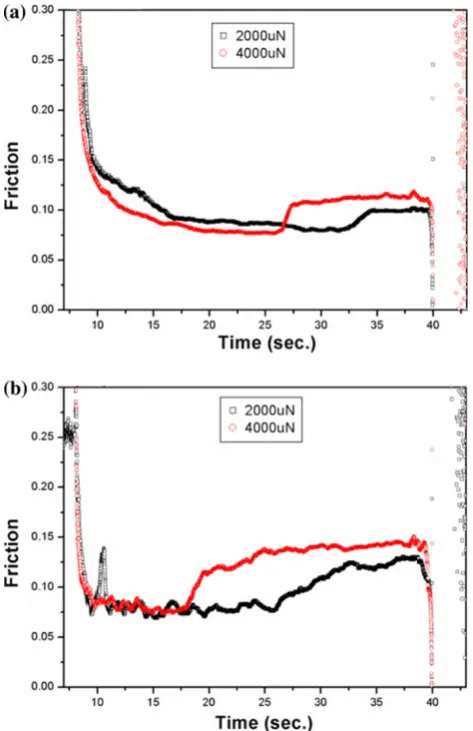
strongly adhesive film providing a slighter fluctuation in itslprofile during the nanoscratch tests (Fig. 2a). Hence, the nanoscratch deformation of the GaN/a-axis sapphire sample resulted inl profiles that featured rather irregular oscillation (Fig.2b). Thus, lower adhesion reflects the presence of interlinks and rearrangements under a higher ramped load, not only involving the weaker GaN bonds but also resulting in higher values of the depth profile and thel values (Table1).
The fluctuation profile from a nanoscratch tests does not depend exclusively on the plasticity or the value ofH; it is also related to the adhesive strength between the film and the substrate. While the contact area between the tool and the GaN surface increases, the pressure under the tool becomes insufficient to drive the transformation to a denser crystal structure. Thus, the deformation theory cannot be accommodated in a ductile manner. From studies of nanomachining processing, both tribological and chemical effects, rather than physical deformation and fracture, are believed to become dominant. In this scenario, the average measured residual stress in the cracking zone is much lower than that in the crack-free zone, because the elastic strain is released by cracking. From the nanotribological point of view, curvature and/or distribution in the values
of lsignal the onset of adhesive failure, such as cracking or delamination resulting from the interaction between the sliding stylus and the debris formed on the nanoscratch track [21,22]. Several factors can affect the value ofHof a film, including the packing factor, stoichiometry, residual stress, preferred orientation, and grain size. In our experi-ments, the orientation of the GaN sample not only affected its nanotribological performance but also its scratching resistance; thus, the volume of the removed material from nanoscratch tests can be measured to determine the role of the orientation of the GaN sample. This approach can be used to explain the nanotribological behavior of the GaN sample; for example, the profile of GaN/a-axis sapphire sample reveals more serious wear of the components (Fig.1) and more unwanted self-excited oscillations (Fig.2) than that of the GaN/c-axis sapphire sample. Thus, the GaN/c-axis sapphire sample revealed relatively small oscillations with respect to the ramped load. Taken toge-ther, our findings reveal that the nanoscratch deformation of the GaN samples was influenced primarily by the ori-entation of the sapphire substrate. The mechanisms for the dislocation recovery from elastic and/or plastic deforma-tion appear to be associated with the activadeforma-tion of dislo-cation sources brought about by the nanoscratching of the Fig. 1 3D AFM images of
scratch tracks formed in GaN films on sapphire substrates:
[image:3.595.204.546.57.398.2]GaN sample. The plastic deformation prior to nanoscrat-ching was associated with the individual movement of a small number of new nucleation sites; large shear stress was quickly accumulated underneath the indenter tip. When the local stress underneath the tip reached high-level cycles, a burst of collective dislocation movement on the slip system was activated, resulting in a release of local stress. The extensive interactions between the dislocations
slipping along the surface of the GaN/a-axis sapphire sample, therefore, confined the brittle transition part of the scratch track, resulting in ductile and/or brittle properties because of the deformed and strain-hardened lattice structure.
Conclusion
We employed a combination of nanoindentation and AFM techniques to investigate the contact-induced deformation behavior of GaN films on c- and a-axis sapphire substrates. We observed three separate scratch processes in the ductile, brittle transition (elastic–plastic deformation), and brittle regions. AFM morphological studies of the bulge edge scenarios provided evidence for significant reductions in the average scratch depth for the GaN/c-axis sapphire. It suggested that the substrate orientation dominated the extent of ploughing in the GaN epilayers during the scratching process. In addition, this discrepancy suggested that c-axis sapphire–grown GaN epilayers have higher shear resistance than those grown on a-axis sapphire. Pile-up events indicated the generation and motion of individual dislocations measured under the critical brittle transition part of the scratch track, result in ductile and/or brittle properties.
Acknowledgments This research was supported by the National Science Council of the Republic of China (NSC-98-2221-E-009-069) and by the National Nano Device Laboratories in Taiwan (NDL97-C04SG-088, NDL97-C05SG-087).
Open Access This article is distributed under the terms of the Creative Commons Attribution Noncommercial License which per-mits any noncommercial use, distribution, and reproduction in any medium, provided the original author(s) and source are credited.
References
1. F.A. Ponce, D.P. Bour, Nature386, 351 (1997)
2. S. Nakamura, T. Mukai, M. Senoh, J. Appl. Phys. 76, 8189 (1994)
3. T. Nagatomo, T. Kuboyama, H. Minamino, O. Omoto, Jpn. J. Appl. Phys.28, L1334 (1989)
4. N. Yoshimoto, T. Matsuoka, T. Sasaki, A. Katsui, Appl. Phys. Lett.59, 2251 (1991)
5. L. Liu, J.H. Edgar, Mater. Sci. Eng. R37, 61 (2002)
6. J.B. Pethica, R. Hutchings, W.C. Oliver, Philos. Mag. A48, 593 (1983)
7. W.C. Oliver, R. Hutchings, J.B. Pethica, inASTM STP 889, ed. by P.J. Blau, B.R. Lawn (American Society for Testing and Materials, Philadelphia, 1986)
8. M.F. Doerner, W.D. Nix, J. Mater. Res.1, 601 (1986)
9. J.B. Pethica, inIon Implantation into Metals, ed. by V. Ashworth, W. Grant, R. Procter (Pergamon Press, Oxford, 1982)
10. J.L. Loubet, J.M. Georges, O. Marchesini, G. Meille, J. Tribol
106, 43 (1984)
[image:4.595.52.289.57.423.2]Fig. 2 Typical profiles of the coefficient of friction (l) plotted with respect to the scratch duration at ramped loads of 2,000 and 4,000lN for GaN films onac-axis andba-axis sapphire substrates
Table 1 Critical lateral forces and values ofl determined from nanoscratch trace depths within GaN films on c- and a-axis sapphire substrates
Sample Normal load (lN)
Coefficient of friction
[image:4.595.50.289.517.600.2]11. D. Newey, M.A. Wilkens, H.M. Pollock, J. Phys. E: Sci. Instrum.
15, 119 (1982)
12. D. Stone, W.R. LaFontaine, P. Alexopoulos, T.-W. Wu, C.-Y. Li, J. Mater. Res.3, 141 (1988)
13. S.O. Kucheyev, J.E. Bradby, J.S. Williams, C. Jagadish, M.V. Swain, G. Li, Appl. Phys. Lett.78, 156 (2001)
14. S.O. Kucheyev, J.E. Bradby, J.S. Williams, C. Jagadish, M. Toth, M.R. Phillips, M.V. Swain, Appl. Phys. Lett. 77, 3373 (2000)
15. R. Nowak, M. Pessa, M. Suganuma, M. Leszczynski, I. Grzegory, S. Porowski, F. Yoshida, Appl. Phys. Lett.75, 2070 (1999) 16. T. Wei, Q. Hu, R. Duan, J. Wang, Y. Zeng, J. Li, Y. Yang,
Y. Liu, Nanoscale Res. Lett.4, 753 (2009)
17. L.L. Sohn, R.L. Willet, Appl. Phys. Lett.67, 1552 (1995) 18. K. Ashida, N. Morita, Y. Shosida, JSME Int. J., Ser. C44, 244
(2001)
19. W. Meredith, G. Horsburgh, G.D. Brownlie, K.A. Prior, B.C. Cavenett, W. Rothwell, A.J. Dann, J. Cryst. Growth 159, 103 (1996)
20. C. Jin, B. Zhang, Z. Ling, J. Wang, X. Hou, Y. Segawa, X. Wang, J. Appl. Phys.81, 5148 (1997)
21. J.M. Sa´nchez, S. El-Mansy, B. Sun, T. Scherban, N. Fang, D. Pantuso, W. Ford, M.R. Elizalde, J.M. Martı´nez-Esnaola, A. Martı´n-Meizoso, J. Gil-Sevillano, M. Fuentes, J. Maiz, Acta Mater.47, 4405 (1999)