International Journal of Emerging Technology and Advanced Engineering
Website: www.ijetae.com (ISSN 2250-2459,ISO 9001:2008 Certified Journal, Volume 3, Issue 12, December 2013)
514
Analysis And Design of Low Power Content Addressable
Memory (CAM) Cell
Yuvana K
1, Balavenkateswarlu P
2, Mohammed Abbas T
3, Ashok S
4 1PG Scholar , 2,3,4Assistant Professor, Vel Tech Multi Tech Dr. Rangarajan Dr. Sakunthala Engineering College, Chennai
Abstract— Content Addressable Memory (CAM) is a high
performance search engine, which access the data based on its contents in a single clock cycle .Due to parallel Match Line(ML) comparison, CAM is Power-Hungry. To overcome this drawback we need to reduce the power consumption of the CAM when we search the data. This paper proposes an idea for improving power and performance of the system. In existing CAM architecture uses basic 10T CAM cell. For this we replace the basic 10T CAM cell with a 4T CAM cell.The proposed XOR CAM of 4T is compared with traditional XOR CAM 10T. The simulation results show the success of the method. This CAM cell is designed using 65nm technology.
Keywords— CAM CELL, Low power, XOR, XNOR, NOR Type, NAND Type.
I. INTRODUCTION
Most memory devices store and retrieve data by addressing specific memory location. As a result, this path often becomes the limiting factor for the systems that rely on fast memory access. The time required to store an item in memory can be reduced considerably if the time can be identified for access by its content rather than by its address. A memory that is accessed in this way is called Content Addressable Memory (CAM). To achieve the effective function of data searching, the data comparison architecture of cam is usually implemented in parallel operation structure. However due to parallel process characteristic, power consumption is always an important concern while designing the CAM circuitry. (i.e.) Content addressable memories simultaneously compare an input word to all the contents of the memory and return the address of matching locations in a single clock cycle.
A CAM architecture is shown in Fig.1. This figure shows a CAM consisting of 4 words, with each word containing 3 bits arranged horizontally (corresponding to 3 CAM cells). There is a match line corresponding to each word. feeding into match line sense amplifiers (MLSAs), and there is a differential search line pair corresponding to each bit of the search word. A CAM search operation begins with loading the data word into the search-data registers followed by precharging all match lines high, putting them all temporarily in the match state.
[image:1.612.343.550.334.479.2]Next, the search line drivers broadcast the search word onto the differential search lines, and each CAM core cell compares its stored bit against the bit on its corresponding search lines. Match lines on which all bits match remain in the precharged-high state. Match lines that have at least one bit that misses, discharge to ground. The MLSA then detects whether its match line has a matching condition or miss condition. Finally, the encoder maps the match line of the matching location to its encoded address.
Fig 1.Block diagram of CAM Architecture
International Journal of Emerging Technology and Advanced Engineering
Website: www.ijetae.com (ISSN 2250-2459,ISO 9001:2008 Certified Journal, Volume 3, Issue 12, December 2013)
515 So we need to explore modifications to it so that area, power and performance can be improved. So we are designing 4 transistor CAM cell[6] such that these can be effectively used in many applications.
II. BASIC CAMCELL
A. OVERVIEW OF CAM AND RAM
The RAM has two major operations: Write and Read. (i.e.) user supplies the memory address and the RAM returns the data stored in that address. A CAM has three major operations: Write, Search and Read.(i.e.)user supplies the data word and CAM search its entire memory to see the supplied data word. If the data word is found, the CAM returns one or more storage address where the word was found. The are two types of CAM .They are Binary CAM (BCAM)and Ternary CAM(TCAM) where BCAM stores 0’s and 1’s and TCAM stores 0’s, 1’s and don’t care. CAM is used in various application like IP Packets in network routers, Broad ATM communication system and Image coding.
B. BASIC OPERATION OF CAM CELL
The basic CAM cell is based on the static memory cell . Data is stored in two cross coupled inverters. The two NMOS transistors controlled by the word line allow the CAM to be written. The four additional transistors used for matching. The bit storage portion is a standard 6T static RAM (SRAM) cell. Hence, this cell performs READ and WRITE operations similar to an SRAM cell. Third operation is MATCH operation.
[image:2.612.384.504.432.553.2]
Fig 2. Block diagram of CAM Cell
For matching a data bit with stored bit. First Leave the wordline low then Precharge match line. Place key on bitline. Match line evaluated.
III. DESIGN OFCAMCELL
A. NAND TYPE CAM CELL (7T)
[image:2.612.95.223.503.617.2]The NAND cell implements the comparison between the stored bit, D, and corresponding search data on the corresponding search lines, (SL,~SL ), using the three comparison transistors M1,MD, and MDB , which are all typically minimum-size to maintain high cell density. We illustrate the bit-comparison operation of a NAND cell through an example[1]. Consider the case of a match when SL =1 and D=1 . Pass transistor MD is ON and passes the logic ―1‖ on the SL to node B. Node B is the bit-match node which is logic ―1‖ if there is a match in the cell. The logic ―1‖ on node B turns ON transistor M1 . Note that M1 is also turned ON in the other match case when SL =0 and D=0. . In this case, the transistor MDB passes a logic high to raise node B. The remaining cases, where SL not equal to D , result in a miss condition, and accordingly node B is logic is ―0‖ and the transistor M1 is OFF. Node B is a pass-transistor implementation of the XNOR function SL xnor D. The NAND nature of this cell becomes clear when multiple NAND cells are serially connected. In this case, the MLn and MLn+1 and nodes are joined to form a word. A serial NMOS chain of all the Mi transistors resembles the pull down path of a CMOS NAND logic gate.
Fig 3. NAND CAM CELL(7T)
A match condition for the entire word occurs only if every cell in a word is in the match condition.
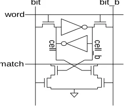
B. NOR TYPE CAM CELL(8T)
The NOR cell implements the comparison between the complementary stored bit, D (and ~D ), and the complementary search data on the complementary search line, SL (and ~SL ), using four comparison transistors, M1 through M4 , which are all typically minimum-size to maintain high cell density.
bit bit_b
word
match
ce
ll cell_
International Journal of Emerging Technology and Advanced Engineering
Website: www.ijetae.com (ISSN 2250-2459,ISO 9001:2008 Certified Journal, Volume 3, Issue 12, December 2013)
516
Fig 4. NOR CAM CELL(8T)
These transistors implement the pull down path of a dynamic XNOR logic gate with inputs SL and D. Each pair of transistors, M1/M3 and M2/M4, forms a pull down path from the match line, ML, such that a mismatch of SL and D activates least one of the pull down paths, connecting ML to ground[1]. A match of SL and D disables both pull down paths, disconnecting ML from ground. The NOR nature of this cell becomes clear when multiple cells are connected in parallel to form a CAM word by shorting the ML of each cell to the ML of adjacent cells. The pull down paths connect in parallel resembling the pulldown path of a CMOS NOR logic gate. There is a match condition given ML only if every individual cell in the word has a match.
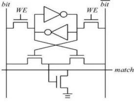
C. XOR AND XNOR CAM CELL(9T)
Basic CAM cell consists of both store unit for storing the data and compare unit for comparing the data as shown in Fig.5a and 5b. Data is stored in two cross coupled inverters. The two NMOS transistors controlled by the word line allow the CAM to be written. The three additional transistors used for matching.
[image:3.612.373.526.148.270.2]
Fig. 5a XOR CAM cell (9T)
Fig. 5b XNOR CAM cell (9T)
The bit storage portion is a standard 6T static RAM (SRAM) cell. Hence, this cell performs READ and WRITE operations similar to an SRAM cell. Third operation is search operation. In Different applications the compare unit can be designed with XOR type or XNOR type blocks[4]. The main operation of CAM cell can be described as: when the cross coupled inverters store the data „1‟ and then the bit and nbit(bit bar/bit) line has the data „1‟ and „0‟ respectively. Now one of the two pull down transistors will be ON state and the other will be OFF state so that there won’t be any transistor path to discharge the match line and hence it remains in High-impedance state. Now if the bit and nbit line has the data „0‟ and „1‟ respectively, then in the compare unit one of the pull down transistor will be in ON state so that the fast pull down transistor moves to ON state. This discharges the match line indicating that the data have been matched.
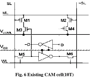
D. EXISTING CAM CELL(10T)
[image:3.612.105.242.510.616.2]International Journal of Emerging Technology and Advanced Engineering
Website: www.ijetae.com (ISSN 2250-2459,ISO 9001:2008 Certified Journal, Volume 3, Issue 12, December 2013)
[image:4.612.90.248.296.430.2]517 The gated-power transistor Px, is controlled by a feedback loop, denoted as ―Power Control‖ which will automatically turn off Px once the voltage on the ML reaches a certain threshold[4]. At the beginning of each cycle, the ML is first initialized by a global control signal EN. At this time, signal EN is set to low and the power transistor Px is turned OFF. This will make the signal ML and C1 initialized to ground and VDD, respectively. After that, signal EN turns HIGH and initiates the COMPARE phase. If one or more mismatches happen in the CAM cells, the ML will be charged up. Interestingly, all the cells of a row will share the limited current offered by the transistor Px, despite whatever number of mismatches.
Fig. 6 Existing CAM cell(10T)
When the voltage of the ML reaches the threshold voltage of transistor M8[4]. Voltage at node C1 will be pulled down. After a certain but very minor delay, the NAND2 gate will be toggled and thus the power transistor Px is turned off again. As a result, the ML is not fully charged to VDD, but limited to some voltage slightly above the threshold voltage of M8[4].
E. MODIFIED CAM CELL (4T)
[image:4.612.358.526.347.499.2]This modified 4T CAM cell design consists of 4 nmos transistors and the cells are arranged such that the two transistors (tc1 and tco) are used to store the data and the remaining two transistors (tw1 and tw0) are used to write the data[8]. The gates of tc1 („a‟) and tco („b‟) are used as storage capacitance elements so that it can be used to store the data.
Fig. 7 XOR CAM cell(4T)
When the transistors tw1 and tw0 are in ON state the data can be transferred to the nodes a and b and then these can be read using transistors tc1 and tc0.
Fig. 8 XNOR CAM cell(4T)
International Journal of Emerging Technology and Advanced Engineering
Website: www.ijetae.com (ISSN 2250-2459,ISO 9001:2008 Certified Journal, Volume 3, Issue 12, December 2013)
518
IV. SIMULATION RESULT AND ANALYSIS
[image:5.612.334.551.123.323.2]Fig .9 Waveform of NAND CAM CELL(7T) circuit in LTspice
[image:5.612.62.275.134.296.2]Fig .10 Waveform of NOR CAM CELL(8T) circuit in LTspice
Fig .11 Waveform of XOR CAM CELL(9T) circuit in LTspice
[image:5.612.59.279.321.701.2]Fig .12 Waveform of Existing CAM CELL(10T) circuit in LTspice
Fig .13 Waveform of XOR CAM CELL(4T) circuit in LTspice Table I
A Power And Delay Comparison
TRANSISTORS POWER(µW) DELAY(ns) POWER DELAY PRODUCT (fJ)
4T XOR CAM (Proposed)
0.4639 1.99675 0.09262*
10T XOR CAM (Existing)
3.8713 2.02593 0.78429*
9T XOR CAM 1.5974 2.00157 0.31973*
7T NAND CAM 5.6906 2.52747 1.43828*
[image:5.612.332.558.349.517.2]International Journal of Emerging Technology and Advanced Engineering
Website: www.ijetae.com (ISSN 2250-2459,ISO 9001:2008 Certified Journal, Volume 3, Issue 12, December 2013)
519 From the simulation report it shows that 4T XOR CAM cell consumes less power and delay when compared to other CAM cell transistor levels.
V. CONCLUSION AND FUTURE WORK
A new XOR CAM Cell 4T have beed designed in this paper. The various design of CAM Cell and proposed XOR CAM is simulated with a 65nm CMOS technology. Further the energy (power-delay product) saved through this circuit is more when compared to the Existing circuit has shown in the table. Therefore the proposed design can be use in low power application of CAM and also in CAM architectures such as Hybrid, Banked and Gated ML sensing technique.
REFERENCES
[1] K.Pagiamtzis and A. Sheikholesami, ―Content addressable
memory (CAM) circuits and architectures: A tutorial and survey,‖ IEEE J. Solid State Circuits, Mar . 2006.
[2] Kuo-Hsing Cheng, Chia-Hung Wei, Jiannchyi Rau,―Design of
Low-Power Content Addressable Memory Cell‖ Solid-State Circuits.
[3] Byung-Do Yang and Lee-Sup Kim, ―A Low-Power CAM Using
Pulsed NAND–NOR Match-Line and Charge-RecyclingSearch-Line Driver‖ IEEE JOURNAL OF SOLID-STATE CIRCUITS, VOL. 40, NO. 8, AUGUST 2005.
[4] Anh-Tuan Do, Shoushun Chen, Zhi-Hui Kong, and Kiat Seng ―A
High Speed Low Power CAM With a Parity Bit and Power-Gated ML Sensing‖ IEEE Trans.Very Large Scale Integr.(VLSI) Syst., VOL. 21, NO. 1, pp.151 -156 JAN 2013.
[5] A. T. Do, S. S. Chen, Z. H. Kong, and K. S. Yeo in ―An and-type
match-line scheme for high-performance energy-efficient content
addressable memories‖Proc. IEEE Int. Symp. Circuits Syst.
(ISCAS), 2011, pp. 2573–2576.
[6] Jose G.Delgado –Frias, Andy Yu and Jabulani Nyathi, ―A Dynamic
Content Addressable Memory Cell‖, in VLSI Systems, Vol 99, No:1, Sep 1999.
[7] N.Mohan and M.Sachdev, ―Low – leakage storage cells for ternary
content addressable memories.‖ IEEE Trans.Very Large Scale Integr.(VLSI) Syst.,May 2009.
[8] Yen-Jen Chang and Yuan Hong Liao Hybrid-type CAM design for
both power and performance efficiency in VLSI systems, Vol No:8,Aug 2008.
[9] Xiao-Liang Tan,Anh-Tuan Do,Shou-Shun Chen,