Study and Design of a Full Bridge DC / DC
Power Converter
E. Baghaz
1,*, S. Bounouar
1, R. Bendaoud
1, B. Zohal
1, N. K. M'Sirdi
2, A. Naamane
2, N. Benaya
3,
N. El Akchioui
3, M. Benhmida
11
Laboratory of Electronics, Instrumentation and Energy (LEIE), Faculty of Sciences, El Jadida, Morocco
2Laboratory of Informatics and Systems, Aix-Marseille University, France
3Laboratory of R&D in Engineering Sciences, Faculty of Sciences and Techniques Al Hoceima,
Abdelmalek Essaâdi University, Morocco
Copyright©2019 by authors, all rights reserved. Authors agree that this article remains permanently open access under the terms of the Creative Commons Attribution License 4.0 International License
Abstract
In this paper, a converter DC/DC for power applications is developed: battery charger for photovoltaic system, vehicle charger, helicopter power supply. It consists of using a Full-Bridge DC/DC converter which is controlled by a new analog control, designed and analyzed during this work. This control has been dimensioned so that it ensures a smooth switching of the transistors, which makes it possible to reduce the losses of power, and consequently increases the efficiency of the overall system. It allows also to increase the current and to lower the voltage to the desired value; a large generated current which reaches 50A.Keywords
Suply Power, DC-DC Converter, PV System, Battery, Efficiency, PWM Signal1. Introduction
Although the field of power electronics has experienced a significant degree of maturity. While, this field suffers from low efficiency and the high cost of electronic circuits. As an example, conventional DC / DC converters (Boost, Buck, ...) are easy to implement, they only require a single PWM signal to control the power switch. While, this type of converters are intended for limited applications in current and voltage [1-4]. To fix this problem, there are several structures of DC / DC converters of alternative power which are used in power applications [8-18].Bor-Ren Lin et al. [17] proposed a full-bridge DC/DC converter with parallel-connected output and
without output inductor, which makes it possible to generate a voltage and a current successively 48V and 20A under a chopping frequency of 100 kHz. This structure has a yield of 90.2%. In the Ref. [18], Texas Instrument has proposed a powerful DC / DC converter structure with a performance of 93%, it can generate a voltage of 12V and a current of 50A. However, in the same reference [18], the authors have not showed and given the operating principle of the UCC28950 command used.
In this context, the study of the functioning a new DC / DC power converter is investigated; It is the full bridge (FB) DC / DC converter [18]. Then, an analog control is developed, which ensures the transistors soft switching. In order to develop a high-performance product, we used high-performance electronic components (transistor and diode) based on silicon carbide. The electrothermal study of these components, allowed us to control their power losses, by following the evolution of their temperature during their operation. The obtained results are compared with those of converter designed and realized by Texas Instrument [18]. This comparison shows that the system designed in this work presents similar results to that of Texas Instrument.
Figure 1. Controlled Full Bridge DC / DC Converter by a Soft Switching Analog Control
2. Converter Full Bridge DC / DC with
a New Analog Control
It is a full Bridge power DC / DC converter (Figure 1), sized according to well-defined specifications, for charging batteries for PV installations. This converter allows to deliver at the output a voltage of 12V, a high current of 50A to accelerate the charging of the batteries, and it operates at a hash frequency. In our contribution, we have developed an analog control, which ensures a smooth control of the six transistors of the converter. In order to improve these performances, we have equipped this converter with silicon carbide-based transistors (C2M0025120D) and diodes (C3D04060A) [22].
2.1. Full Bridge DC/DC Converter
2.1.1. Description of the Full Bridge DC / DC Converter Figure 2 shows a DC / DC converter phase shifted in full bridge. As the transistors TA, TB, TC, and TD form the
complete bridge on the primary side of the transformer T2,
they switch with a duty cycle of almost 0.5. Next, TE, and
TF represent the transistors on the secondary side of the
transformer T2.While, LOut and COut form the output filter.
The inductance Lr is intended to assist the T2 transformer
leakage inductance, during resonant operation with the internal capacitance of the Mosfet, and facilitates zero voltage switching (ZVT).Then, in order to design a high-performance product, we used silicon carbide-based transistors (C2M0025120D). To follow their operations, we carried out an electrothermal study of this transistor
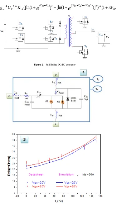
(figure 3 and 4), which allows us to follow the evolution of the junction temperature during its operation. From Figure 3A, we deduce the equation of the current drain-source (IDS) of the transistor Eq.(1), which is the difference between the direct current IG1 Eq.(2) and the inverse one IG2 Eq.(3) [20].
(1)
(2)
(3) By replacing equations (2) and (3) as well as the formula of the nip (Vp) in that of (1), we obtain the final equation of the current Drain-Source (Ids) Eq.( 4) [ 21].
Figure 3B shows the results of simulation and those of datasheet [22], the variation of the resistance Drain-Source (Rdson) as a function of the temperature, for a value of current of 50A. It appears that the electrothermal model developed during this work has a precision close to the optimal operating conditions (datasheet), even in the case of very high temperatures (150 ° C), which confirms the characteristic of operation at high temperature. SIC transistors. Then, in Fig. 3C, we have represented the variation of the drain-source current (Ids) as a function of the voltage at the output of the transistor SIC (Vds) for different Grid-Source voltage values (Vgs) and a temperature of 25 °. C. It appears that there is a very good agreement between the simulation results, represented by lines, and those of datasheet, represented by lines.
1
(
)
2(
)
DS G P s G P D
I
=
I
V
−
V
−
I
V
−
V
2 1 *[ln(1 exp[ ])]
2 *
P s
G S
T
V V
I =I + −
U
2
2
*[ln(1 exp[
])]
2 *
P D
G S
T
V
V
I
=
I
+
−
(4)
Figure 2. Full Bridge DC/DC converter
( ) (( ) * )
2 2 2
2 *
*
*
([ln(1
VDS Vth]
[ln(1
VDS Vth n VDS)] ) * (1
)
DS m T S DS
I
g
U
K
e
e
V
α
λ
− − −
[image:3.595.122.494.71.722.2]Figure 3. A: Electrical model of the power transistor SIC (C2M0080120D), B: Variation of resistance Rdson as a function of the junction temperature,
C: Variation of Ids current as a function of Vds, for different values of Vgs
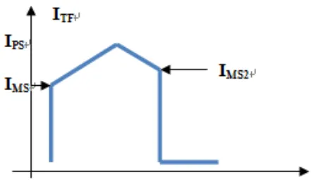
Figure 4. Form of the current of the transistor TF of
Figure 2
2.1.2. Dimensioning of the Full Bridge DC / DC Converter Based on the reference [18], we have dimensioned the Full Bridge converter of figure 2 according to the specifications of this application: a continuous input voltage of 410V, hashing frequency of 100 kHz transistors, a voltage 12V output and 50A output current.
Calculation of the Different Elements of the Transformer T2
Transistor transformation ratio (n): is calculated
from equation 5: VINMIN is the minimum input voltage
(410V), VRdson is the voltage drop of the transistor, it
is estimated to be 0.3V, αMax is the value of the
maximum duty cycle and VOut is at the output voltage
of the DC / DC converter.
(5)
Typical cyclical report: it is the duty cycle of the
PWM signals which controls the transistors on the secondary side of the transformer (TE and TF).
(6)
Ripple of inductor current LOut: it represents 20%
of the total current at the output of the DC / DC converter.
(7)
Transformer magnetization inductance: it allows
reducing the increase of the magnetization current resulting from the increase of the signal Cs (figure 1). Its value is calculated by the following equation, Fsw is the frequency of hashing of the transistors (100kHz).
(8)
Calculation of the Filter Elements in the Output
Output inductance (LOut): it represents one of the
elements of the RC filter at the output of the converter.
(9)
Capacitor at the output (COut): it is based on the
ripple of the output voltage of the DC / DC converter.
(
2 *
) *
21
INMIN Rdson Max
P
N Out Rdson
V
V
N
n
N
V
V
α
−
=
=
=
+
(
) *
0.64
(
2 *
)
Out Rdson
Typ
IN Rdson
V
V
n
V
V
α
=
+
≈
−
600
* 0.2
* 0.2 10
12
Out Lout
Out
P
I
A
V
∆
=
=
=
* (1
)
2.92
* 0.5
* 2 *
IN Typ
MAG
Lout
SW
V
L
mH
I
F
n
α
−
≥
∆
=
* (1
)
2
* 2 *
Out Typ
Out
Lout SW
V
L
H
I
F
α
µ
−
=
=
[image:4.595.61.285.336.469.2]The time required for the LOut to change 90% of its
current is described by the following equation:
(10)
In the following equation (11), we considered that 90% of the output voltage ripple (VOnd) is due to the internal
resistance of the COut capacitance and the COut capacitance
occupies 10% of this ripple.
(11)
Equations concern the currents of transistors TE
and TF on the secondary side
The signal form of the current flowing in the transistor TF is represented in FIG. 4. The quantities IPS, IMS and IMS2
are represented by the following equations:
(12)
(13)
(14)
2.2. Analog Control Design with Soft Switching
The analogcontrol designed in this work is based on the image of the input generator current and the output voltage of the DC / DC converter.
2.2.1. Dimensioning of the Analog Control
In order to design a simple analog control, adaptable to high power applications and meeting the great challenges of power electronics, we have designed an analog control that consists of:
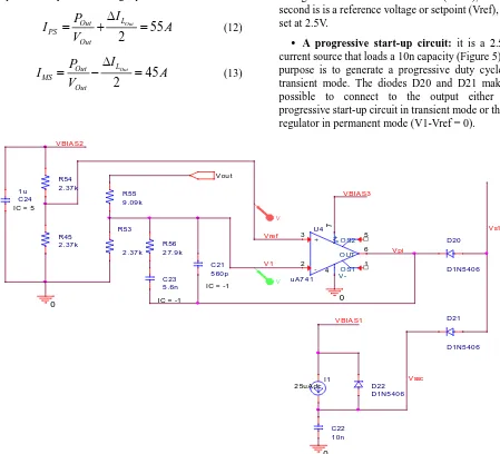
A proportional and integral PI controller: it
consists of regulating the output voltage to a given reference. As shown in Figure 5, the proportional and integral amplifier PI is connected to its input two signals: the first is a fraction (V1) of the output voltage of the DC / DC converter (VOut), and the second is is a reference voltage or setpoint (Vref), it is set at 2.5V.
A progressive start-up circuit: it is a 2.5μA
[image:5.595.74.523.326.734.2]current source that loads a 10n capacity (Figure 5), its purpose is to generate a progressive duty cycle in transient mode. The diodes D20 and D21 make it possible to connect to the output either the progressive start-up circuit in transient mode or the PI regulator in permanent mode (V1-Vref = 0).
Figure 5. Proportional Regulator and Connected Integral of a Progressive Load Circuit
1
*
* 0.9
7.5
Out Out Out OutL
P
V
t
S
V
µ
=
=
1* 0.9 *
5.6
* 0.1
Out Out Out ondP
t
V
C
mH
V
≥
=
55
2
Out L Out PS OutI
P
I
A
V
∆
=
+
=
45
2
Out L Out MS OutI
P
I
A
V
∆
=
−
=
250
2
Out L MS PSI
I
=
I
−
∆
=
A
V
V
U4
u A7 4 1 + 3 -2 V+ 7 V -4
O UT 6
O S1 1 O S2 5
V s1
C21 5 60 p
IC = -1 R45
2 .37 k
V BIA S3
D20
D1N5 40 6
0
C23 5 .6n
IC = -1 R53
2 .37 k V pi
V 1
0
V re f V BIA S2
R54 2 .37 k
C24 1 u
IC = 5
R55 9 .09 k
R56 2 7.9 k
V ou t
D21
D1N5 40 6
D22 D1N5 40 6 I1
2 5u A dc
V ssc
C22 1 0n
V BIA S1
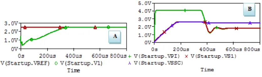
Figure 6. Signals Generated by the Circuit of Figure 5
We have shown in Figure 6, the simulation results, using the Pspice software. It appears that, at the transient (0 to 0.5ms), we see that in Figure 6A, the reference voltage or setpoint is set (Vref) at 2.5V. However, the voltage V1, is a fraction of the output voltage of the converter (VOut), increases gradually by almost 1V until it merges with the reference voltage. Beyond 0.5ms (steady state), it is clear that the difference between the two signals V1 and Vref is zero. Then, it is noted in FIG. 6B that the voltage Vs1 (in red), at the circuit output of FIG. 5, is equal to that generated by the progressive charging circuit VSSC (in purple). The voltage at the output of the regulator PI is equal to that of the power supply (3.2V) (in green). While at steady state, the voltage Vs1 is equal to that generated by the regulator PI (2.4V).
The acquisition of current was performed using a transformer with a transformation ratio (m) of 100 and the maximum voltage applied to the CS pin is Vp = 2V. From these data, we calculate the values of the resistors (R1 and Rcs) of Figure 7:
Figure 7. Input current acquisition circuit
(15)
Knowing that the nominal peak current (Ip1) is described by the following equation:
(16)
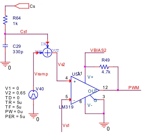
(17) The signal representing the current image at the input of the Full Bridge DC / DC converter is added to a sawtooth signal (Vramp) (Figure 8), using a summator. Then, the obtained signal is compared with the generated signal Vs1 by the circuit of FIG. As a result, this comparison results in a PWM signal.
0
CS
Rcs D20
DN4 1 48
T 1
N = 1 00
R1
V in p ut
4 10 V dc
0 DC/DC Con verte r
1
(
0.3)
20.89
(
*1.1)
p CS
p
V
R
I
n
−
=
=
Ω
1 1
*
1
(
) *
6.88
*
2
* 2 *
INMIN MAX
L p
MAG SW
V
D
I
Ps
I
Vs
η
m
L
F
∆
=
+
+
=
7
*
CS800
[image:6.595.88.532.356.633.2]Figure 8. Comparison of the Image Signal of the Input Current with the Signal Vs1 of Figure 6
2.2.2. Validation the Dimentioning of the Analog Control with Soft Switching
In order to validate our study concerning the analog control, some have been done on PsPice; the results are shown in Figure 9.
Figure 9. Generated Signals by the circuits of Figures 7 and 8: C: Signal Cs, image of the current at the input of the DC / DC converter (in green) and that in sawtooth (in purple); D: Comparison between a signal Vs2 of Figure 8 with that Vs1 of Figure 5; E: PWM signal at the output of the comparator of Figure 8
V s1 V ra m p
P WM U5A
L M3 1 9
O UT 1 2
+
4
-5
G 3
V +
1 1
V
-6
V BIA S2
R49
4 .7k
0
IN1 OUT IN2
R64 1 k
Cs1
C29 3 30 p
0
Cs
0
V 40
T D = 0
T F = 5u P W = 0 u P ER = 5 u V 1 = 0
T R = 5u V 2 = 0.6 5
[image:7.595.179.417.377.716.2]By connecting the PWM signal of Figure 9 E to the Flip Flop JK flip-flop input (Figure 10), its Q output changes the state only if the PWM signal connected to its CLK input is at the rising edge (Figure 11F). In order to ensure ZVS switching (soft switching), we applied a 360ns delay to the rising edge of two Q and 𝑄� of Flip Flop JK (Figure 11 G and H), this allows us to have two PWM signals QC and QD of the transistors TC and TD of Figure 2.
Figure 10. PWM signals connected to transistors TC and TD
Figure 11. Circuit signals of Figure 10: F: PWM CLK signal flip flop JK (pink) and the output Q (green); G: Q signal shifted by 360ns (in red); H: PWM signal Q ̅ (in red) shifted by 360ns
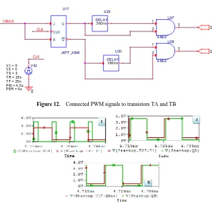
Following the same principle, we generated the other two PWM signals from the second arm of the Full Bridge DC / DC converter (Figure 12). Such as, by connecting a CLK signal with a duty cycle of 0.05 to the CLK input of the Flip Flop JK, resulting in two Q and Q� outputs. By imposing a 360ns delay on the rising edge of each output in the same way, we deduce the other two PWM signals (QA and QB) from the primary part. FIG. 13 represents the simulation results of the signals generated by the circuit of FIG. 13.
U21
JKFF_A B M
J CLK K
Q
Q
P WM V BIA S
U11
A ND2
1 2
3
U12
A ND2
1 2
3
Q C
Q D
U25
3 60 n s
DEL A Y
U26
3 60 n s
[image:8.595.112.487.136.266.2] [image:8.595.179.417.293.630.2]Figure 12. Connected PWM signals to transistors TA and TB
Figure 13. I: connected CLK signal (in green) to the input of Flip Flop JK and the output (in red); J: PWM signal QA (in green) obtained by shifting each rising edge of the signal to the output Q of the flip-flop JK (in red); K: PWM signal QD (in green) obtained by shifting each rising edge of the signal to the output (Q) ̅ of the JK flip-flop (in red)
The circuit of FIG. 15 makes it possible to generate two PWM signals, which control the transistors on the secondary side of the transformer (TE and TF) of FIG. 2. It consists in connecting the two PWM Out C and Out A signals to the two R inputs. And S of an RS flip-flop. The results obtained are shown in FIG.
Figure 14. Connected PWM signals to transistors on the secondary side of the transformer
Figure 15. Signals of the circuit of Figure 16: L: PWM Signal QA and QC are connected to the input of an RS flip-flop. M: PWM signal Out E which controls the transistor TE of FIG. 2. N: PWM signal QB and QD are connected to the input of an RS flip-flop. O: PWM signal Out F which controls the transistor TF of FIG 2
U27
A ND2 1 2
3
U28
A ND2 1 2
3 U29
3 60 n s DEL A Y
U30 3 60 n s DEL A Y
Q B Q A
CLK V BIA S
U17
JKFF_A B M
J
CLK
K Q
Q
0 V 42 T D = 0 T F = 25 n P W = 4 .5 u P ER = 5 u V 1 = 5 T R = 25 n V 2 = 0
CLK
U4
RSFF
S E
1
CLK
2
RE
3
Q 4
Q 5
U5
RSFF
S E
1
CLK
2
RE
3
Q 4
Q 5
V BIA S2 V BIA S2 O UT A
O UT C O UT D
O UT B
[image:9.595.140.461.81.207.2] [image:9.595.145.427.457.542.2] [image:9.595.157.440.573.715.2]Figure 16. Complete Circuit of the Switching Power Supply Designed 0 0 0 C19 5n U37 C3D10065A A 1 K 2 CASE 3 C20 5n U38 C3D10065A A 1 K 2 CASE 3 L3 2uH L6 26uH I V V V V C15 5n C16 5n C17 5n C3_2
ESR = 0.01
X = 1 C = 330u
IC = 400
C18 5n
V1 410Vdc
OUT C U39
C2M 0080120D D 1 G 2 S 3
T J 4 T C 5
U40 C2M 0080120D D 1 G 2 S 3
T J 4 T C 5
U41 C2M 0080120D D 1 G 2 S 3
T J 4 T C 5
U42 C2M 0080120D D 1 G 2 S 3 T J 4
T C 5
R52 240m CS VOUT V2 25Vdc V3 25Vdc V4 25Vdc V5 25Vdc 0 0 R1_2 8 0 0 0 U6 IR2111 1 1 2 2 3 3 U7 IR2111 1 1 2 2 3 3 0 0 OUT F D1 DN4148 Q6 FDP032N08 Q5 FDP032N08 T 1
N = 100 R2_2
4.87k
C14 125m D11
M URS360T 3 D5 M URS360T 3
OUT E OUT B OUT A VOUTP CS Startup Startup Cs Vout QC QD QA QB OUT C OUT D U43 RSFF SE 1 CLK 2 RE 3 Q 4 Q 5 U44 RSFF SE 1 CLK 2 RE 3 Q 4 Q 5 VBIAS2 VBIAS2 OUT A OUT C OUT B
OUT D OUT F OUT E V37 5Vdc VBIAS2 0 U22 C3D10065A A 1 K 2
CASE 3 T 2
LLEAK = 7.5u NP1 = 21
RP1 = 0.215
LM = 2.6m NS1 = 1
RCORE = 100K RS1 = 0.58m
NS2 = 1
RS2 = 0.58m U2 IR2111 1 1 2 2 3 3 U3 IR2111 1 1 2 2 3 3 U4 IR2111 1 1 2 2 3 3 U5 IR2111 1 1 2 2 3 3 U23 C3D10065A A 1 K 2 CASE 3 OUT A OUT B OUT D U24 C3D10065A A 1 K 2
CASE 3 U25
C3D10065A
A
1 K
2
[image:10.808.54.769.78.471.2]3. Results and Interpretations
Figure 16 shows the complete circuit of the switching power supply, implanted in the Pspice simulator. The different values of each electronic component used were defined based on the theoretical study of paragraph II.1.2.We represent in the following, the different simulation results obtained.
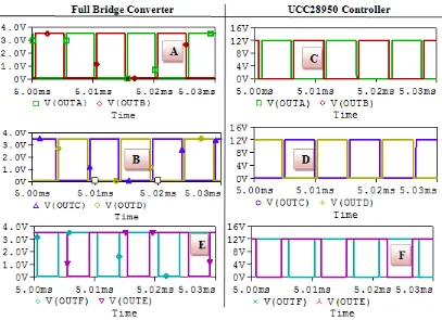
3.1. Comparison of the Performance of the Designed Controller and Those of the UCC28950 Controller
We have shown in Figure 17 on the left, the different signals delivered by the DC / DC conversion system designed in this work. On the same figure on the right, we have represented the same signals generated by the Full Bridge DC / DC converter, designed by Texas Instrument [18]. The purpose of this comparison is to clearly show the qualities of the product designed in in work. The results obtained show that:
The signals PWM OUTA, B, C and D generated by the two systems show that they have the same duty cycle of 0.47, the same frequency of 100 kHz. The difference in amplitude is explained by the fact that the PWM signals of the designed control have been visualized at the output of the AND gate of FIGS. 11 and 13, the maximum amplitude that can reach is 3.5V. So to amplify this amplitude, we used a driver IR2111, which allows to play a role of an adapter between the control part and the power part (DC / DC converter).
The PWM OUTE, F signals generated by the two commands have the same duty ratio of 0.62, which validates the theoretical value calculated by equation 2, which is 0.63.
Figure 17. PWM OUT signals A, B, C and D on the primary side and those on secondary side OUTE, F are generated by the designed control (Figure 17A, B and E) and those generated by UCC28950 (Figure 17C, D and F).
[image:11.595.95.502.313.608.2]Figure 18. Voltages and currents at the input and at the output of the transformer of the DC / DC converter are generated by the designed control on the left and those generated by UCC28950 on the right: A and B: Voltage at the input of the transformer; C and D: Current at the input of the transformer; E and F: Current at the output of the transformer.
The currents (figure 19 A and B), which flow in the inductance of the output of the DC / DC converter, of two commands are identical. Then, its ripple equals to 11A, which corresponds to that of equation 3, it is of the order of 10A.
[image:12.595.87.494.82.499.2] [image:12.595.285.495.595.727.2] The voltage, current and power generated by the DC / DC conversion system designed (Figure 20 A and B) are successively 12V, 50A and 600W. They are identical with those generated by the UCC28950 (Figure 20 C and D).
Figure 20. Electrical quantities at the output of the DC / DC converter generated by the two commands:A (C): Voltage and Current Generated by Analog Control (UCC28950) B (D): Power generated by the analog control (UCC28950) E (F): Overall efficiency of the converter controlled by the analog control (UCC28950)
The efficiency presented by the system developed during this work is of the order of 92% (Figure 21E), it is almost identical to that generated by the Texas Instrument system, which is 93% (Figure 21F).
Figure 21. Overall efficiency of the converter controlled by the analog control (UCC28950)
3.2. Losses in a Transistor of the DC / DC Converter Controlled by the Analog Control
This study consists of studying the losses of powers dissipated in each transistor of the designed converter. We have shown in FIG. 22 the current of the drain C and the voltage VDS of the transistor TA of the DC / DC converter of FIG. 3. It should be noted that the current is multiplied by 100 times in order to clearly note the power losses during transistor switching. It seems that:
[image:13.595.91.501.116.334.2] [image:13.595.70.505.410.552.2]Figure.22. Vds voltage and Id current of the transistor TA of the DC / DC converter of Fig. 3. A and B: Vds voltage and current Id at the opening and closing of the transistor. C: Loss dissipated in the transistor TA.
4. Conclusions
In this paper, we have designed a high current DC / DC converter for PV applications. It is dimensioned based on the following specifications: a voltage of 12V, a current of 50A, and a hash frequency of 100 kHz. It is a full-frame DC / DC converter controlled by an analog control, developed and designed during this work. This application is specially developed for PV lighting installations, it ensures a large current adjustable according to the voltage of the batteries (12V, 24V, ...), which ensures a fast charge of the batteries. In order to improve its efficiency, we have equipped this converter with power switches based on silicon carbide. The electrothermal study carried out of the transistor used (C2M0025120D) makes it possible to clearly show these advantages with respect to the other families of transistors, which are a high response time and a high temperature resistance.
The results obtained show, on the one hand, that the product designed has efficiency, and on the other hand that they are comparable with those of the Texas Instrument converter.
REFERENCES
M. Melhaoui, E. Baghaz, K. Hirech, M. F. Yaden and K. [1]
Kassmi. Contribution to the improvement of the MPPT control functioning of Photovoltaic systems. International Review of Electrical Engineering (I.R.E.E.), v. 9, n. 2, p. 393-400, apr. 2014. ISSN 1827-6679.
E. Baghaz, M. Melhaoui, F. Yaden, K. Hirech, K. [2]
Kassmi.Design, realization and optimization of the photovoltaic systems equipped with analog and digital MPPT commands .Energy Procedia 42 (2013) 270 – 279.
Elhadi BAGHAZ.Architectures discrétisées de gestion de [3]
l’énergie fournie par les systèmes photovoltaïques. Thèse soutenue à l’université Mohamed Premier d’Oujda, Juin 2015.
E. Baghaz, M. Melhaoui, K. Kassmi .Design and Realization [4]
of a Discretized Photovoltaic System. Universal Journal of Electrical and Electronic Engineering Vol. 2(2), pp. 70 – 80, 2014.
Joydip Jana, Hiranmay Samanta, Konika Das Bhattacharya, [5]
Hiranmay Saha. Design and development of high efficiency five stage battery charge controller with improved MPPT performance for Solar PV Systems. International Journal of Renewable Energy Research, Vol.8, No.2, June, 2018.
Bassim M.H. Jassim, Harith Mohammed Jasim.Modelling of [6]
a Solar Array Simulator based on Multiple DC-DC Converters. International Journal of Renewable Energy Research, Vol.8, No.2, Jun, 2018.
T. Arunkumari, V.Indragandh.A Novel Single Switch High [7]
Step Up DC-DC Converter for PV BAsed Application. International Journal of Renewable Energy research,Vol. 8, No. 2, June, 2018.
L. Balogh, “The current-doubler rectifier: An alternative [8]
rectification technique for push-pull and bridge converters,” Unitrode Integrated Circuit Corporation, Design note, DN-63, 2001, pp. 1–5.
L. Balogh, “Design Review: 100 W, 400 KHz DC-DC [9]
converter with current doubler synchronous rectification achieves 92% efficiency”. Texas Intrument, Design Review, 2001, pp.1–40.
N.H. Kutkut, D.M. Divan, R.W. Gasjoigne, “An improved [10]
full bridge zero voltage switching PWM converter using a two inductor rectifier,” IEEE Trans. Ind. Applicat., vol. 31, n°. 1, pp. 119–126, Jan. /Feb. 1995.
R. Redl, L. Balogh, D.W. Edwards, “Optimum ZVS [11]
APEC’94, 1994, vol. 1, pp. 159–165.
L. Zhao, H. Li, Z. Li, “High efficiency variable-frequency [12]
full-bridge converter with a load adaptive control method based on the loss mode,’’ Energies, vol. 8, 2015, pp. 2647– 2673.
D. R. Strek, “Compact isolated high frequency DC/DC [13]
converters using self driven synchronous rectification,” PhD Virginia Polytechnic Institute and State University, 2003.
S. Cetin, “Performance analysis of a self driven phase shifted [14]
full bridge converter for data center applications, ‘Advances in Engineering Mechanics and Materials, p. 41–43.
Z. Sun, B. Eng, “Full bridge DC/DC converter with zero [15]
current switching synchronous rectification for auxiliary power units,”McMaster University, 2014.
M. O’Loughlin, “UCC28950 600-W, phase-shifted, [16]
full-bridge application report,” TI Lit. No. SLUA560B, pp. 1–30, Sept. 2010.
Lin, B.R., Shiau, T.Y ‘Zero-voltage switching full-bridge [17]
DC/DC converter with parallel-connected output and without output inductor’, IET Power Electron., 2013, 6, (3), pp. 505–515.
http://www.ti.com/lit/ds/symlink/ucc28950.pdf,January,201 [18]
9.
http://www.wolfspeed.com/media/downloads/161/C2M002 [19]
5120D.pdf, January, 2019.
Matthias Bucher, Christophe Lallement and Christian C. Enz. [20]
An Efficient Parameter Extraction Methodology for the EKV MOST Model. Proc. 1996 IEEE Int. Conference on Microelectronic Test Structures, Vol. 9, pp. 145-150, Trento, Italy, March 26-28, 1996.
Bejoy N. Pushpakaran, Stephen B. Bayne, Gangyao Wang, [21]
John Mookken. FAST AND ACCURATE
ELECTRO-THERMAL BEHAVIORAL MODEL OF A
COMMERCIAL SiC 1200V, 80 mΩ POWER MOSFET.