Georgia State University
ScholarWorks @ Georgia State University
Physics and Astronomy Dissertations
Department of Physics and Astronomy
12-17-2015
Optical and Transport Properties of Quantum
Dots in Dot-In-A-Well Systems and Graphene-Like
Materials
Venkata Chaganti
Follow this and additional works at:
https://scholarworks.gsu.edu/phy_astr_diss
This Dissertation is brought to you for free and open access by the Department of Physics and Astronomy at ScholarWorks @ Georgia State University. It has been accepted for inclusion in Physics and Astronomy Dissertations by an authorized administrator of ScholarWorks @ Georgia State University. For more information, please [email protected].
Recommended Citation
Chaganti, Venkata, "Optical and Transport Properties of Quantum Dots in Dot-In-A-Well Systems and Graphene-Like Materials." Dissertation, Georgia State University, 2015.
OPTICAL AND TRANSPORT PROPERTIES OF QUANTUM DOTS IN DOT-IN-A-WELL
SYSTEMS AND GRAPHENE-LIKE MATERIALS
by
VENKATA CHAGANTI
Under the Direction of Vadym Apalkov, PhD
ABSTRACT
Quantum dots exhibit strongly size-dependent optical and electrical
properties. The abilityto join the dots into complex assemblies creates many opportunities for scientific discovery. This motivated our present research work on QDIPs, DWELLs, and graphene like QDs. The intention of this research was to study the size dependent achievements of QDIPs, DWELLs, and graphene like QDs with those of competitive technologies, with the emphasis on the material properties, device structure, and
their impact on the device performance.
self-assembled QD structure is analyzed theoretically with twenty-hole levels (Intraband optical transitions within the valence band) and twenty-electron energy levels (DWELL). Continuing the efforts to study self-assembled QDs we extended our work to graphene like quantum dots (graphene and germanene) to study the electronic transport properties.
We study numerically the intraband optical transitions within the valence band of InxGa1-xAs/GaAs pyramidal quantum dots. We analyze the possibility of tuning of corresponding absorption spectra by varying the size and composition of the dots. Both ‘x ’ and the size of the quantum dot base are varied.
We have found that the absorption spectra of such quantum dots are more sensitive to the in-plane incident light.
We present numerically obtained absorption optical spectra of n-doped InAs/In0.15Ga0.85As/GaAs quantum dot-in-a-well systems. The absorption spectra are mainly determined by the size of the quantum dot and have weak dependence on the thickness of the quantum well and position of the dot in a well. The dot-in-a-well system is sensitive to both in-plane and out-of-plane polarizations of the incident light with much stronger absorption intensities for the in-plane-polarized light.
We also present theoretically obtained I-V characteristics of graphene quantum dots, which are realized as a small piece of monolayer graphene. We describe graphene within the nearest-neighbor tight-binding model. The current versus the bias voltage has typical step-like shape, which is due to discrete energy spectrum of the quantum dot. The current through the dot system also depends on the position of the electrodes relative to the quantum dot.
Application of external electric field results in rotation of electron spin by approximately 0.50, where the direction of rotation depends on the electron energy.
INDEX WORDS: Quantum Dots, Quantum Dot Infrared Photodetector, Quantum Dot-in-a-well
OPTICAL AND TRANSPORT PROPERTIES OF QUANTUM DOTS IN DOT-IN-A-WELL
SYSTEMS AND GRAPHENE-LIKE MATERIALS
by
VENKATA CHAGANTI
A Dissertation Submitted in Partial Fulfillment of the Requirements for the Degree of
Doctor of Philosophy
in the College of Arts and Sciences
Georgia State University
Copyright by
Venkata R Chaganti
OPTICAL AND TRANSPORT PROPERTIES OF QUANTUM DOTS IN DOT-IN-A-WELL
SYSTEMS AND GRAPHENE-LIKE MATERIALS
by
VENKATA CHAGANTI
Committee Chair:
Vadym Apalkov
Committee:
Unil Perera
Mukesh Damala
Ramesh Mani
Russel White
Brian Thoms
Electronic Version Approved:
Office of Graduate Studies
College of Arts and Sciences
Georgia State University
iv
DEDICATION
I dedicate my dissertation to God, family and friends. A special feeling of gratitude to my
elder sister Surya Kumari whose words of encouragement and push for tenacity ring in my ears.
Special thanks to my younger sister and my mother for their continuous support and
encouragement. A heart filled thanks to my friends who have helped me and driven me the extra
mile to complete my work in time. There are no words to complete my expression for the support
given by my family.
v
ACKNOWLEDGEMENTS
Firstly, I would like to express my sincere gratitude to my advisor Prof. Vadym Apalkov
for the continuous support of my Ph.D. study and research work.
I would like to thank the rest of my thesis committee: Prof. Unil Perera, Prof. Ramesh
Mani, Prof. Mukesh Dhamala, Prof. Brian Thoms, and Prof. Russel White for their insightful
comments and encouragement.
My sincere thanks also goes to Prof. Steve Manson, Prof. Stockman, and Prof. Dietz, who
provided me an opportunity to take their classes.
I thank all my fellow graduates Mr. Sampath, Ms. Indika, Ms. Thakshila, Dr. Sahil, Dr.
Chand, Mr. Jitto and specially Dr. Mohammad Javani who helped me all these years with most
useful stimulating discussions. I thank the rest of the graduate students who have been supportive
vi
TABLE OF CONTENTS
ACKNOWLEDGEMENTS ... v
LIST OF TABLES ... ix
LIST OF FIGURES ... x
1
INTRODUCTION... 1
1.1
Quantum dots as artificial atoms ... 1
1.2
Quantum dot infrared photodetectors ... 5
1.3
Graphene quantum dots ... 10
1.4
Buckled graphene-like materials ... 13
1.5
Data Collection and Analysis Methods ... 15
1.5.1
All about NEXTNANO Software Package ... 15
1.5.2
All about Matlab ... 17
1.5.3
FORTRAN ... 18
2
RESULTS ANS DISCUSSIONS ... 19
2.1
Research Questions ... 19
2.2
Intraband Optical Transition in InGaAs/GaAs Pyramidal Quantum Dots . 21
2.2.1
Model and Main Equations ... 21
2.2.2
Results and Discussion ... 24
2.3
Optical properties of dot-in-a-well systems ... 33
vii
2.3.2
Results and Discussion ... 37
2.4 I-V Characteristics of Graphene Quantum Dots ... 47
2.4.1 Model and Main Equations ... 47
2.4.2. Results and Discussion ... 50
2.5 Germanene quantum dots: energy spectrum and spin texture ... 56
2.5.1 Model and Main Equations ... 56
2.5.2 Results and Discussions ... 58
3
CONCLUSIONS AND RECOMMENDATIONS ... 68
3.1.1
Recommendation(In
xGa
1-xAs/GaAs quantum dot) ... 69
3.2
Conclusions and Recommendations for “Theoretical study of intraband
optical transitions in conduction band of a dot-in-a-well system”... 69
3.2.1
Recommendations (DWELL) ... 70
3.3
Conclusions and Recommendations for “I-V characteristic of graphene
quantum dots and molecules” ... 70
3.3.1
Recommendations (I-V characteristics of Graphene quantum dot) ... 70
3.4
Conclusions and Recommendations for “Germanene quantum dots: energy
spectrum and spin texture” ... 71
3.4.1
Recommendations (Silicene and Germanene quantum dots) ... 71
3.5
Overall conclusions of Dissertation ... 72
ix
LIST OF TABLES
Table 1Pyramidal quantum dots dimensions………22
Table
2Parameters
of
In
xGa
1-xAs
pyramidal
quantum
dots………..22
Error! Bookmark not defined.
Table 3Parameters of the 8x8 kp model………23
Table4 First intensity peak positions……….27
Table5 Second peak intensity positions ………27
Table6 Dimensions for dot-in-well ………...36
Table7 Parameters of DWELL ……….36
Table8 Optical Transitions for Two peaks for x- polarized light………..41
x
LIST OF FIGURES
Figure 1 Density of States in
Semiconductor………..3Error! Bookmark not defined.
Figure 2 Buckled Silicene / Germanene Structure……….13
Figure 3Shape and position of Pyramidal QD.………..17
Figure 4X-polarized Optical Transitions for QD for x = 0.7……….22
Figure 5X-polarized Optical Transitions for QD for x = 1.0……….22
Figure 6Z-polarized Optical Transitions for x = 0.7………..25
Figure 7Z-polarized Optical Transitions for x = 1.0………..25
Figure 8Ratio of Intensities Ix/Iz for the QD……….26
Figure 9First moment for X-polarized light for QD………..27
Figure 10Second moment of X-polarized light for QD……….28
Figure 11Second moment of Z-polarized light for QD……….28
Figure 12Schematic illustration of the dot-in-a-well system……….31
Figure 13Absorption spectra for x-polarized light for dot-in-a-well system……….34
Figure 14Absorption spectra of DWELL system for x&z polarized light……….35
Figure 15First moments of x&z polarized light of DWELL……….38
Figure 16Second moment of the x-polarized light………40
Figure 17Second moment for z-polarized light of DWELL………..41
Figure 18Ratio of intensities of Ix/Iz of the DWELL………42
Figure 19Schematic view of graphene quantum dot and molecule………...44
Figure 10 I-V characteristic of graphene QD………47
xi
Figure 12Saturation Current of QD and molecule………...49
Figure 13Difference in Current……….50
Figure 14Germanene QD………..52
Figure 15Energy Spectra of Germanene………...55
Figure 16 Spin angle as a function of E………56
Figure 17 In-plane component of the spin for different values of E……….58
Figure 18 Spatial distribution of in-plan component of spin………...60
Figure 19 Tunneling current through 13 atoms Germanene………...61
Figure 20 Tunneling current through 27 atoms Germanene………...62
1
1 INTRODUCTION
1.1 Quantum dots as artificial atoms
My research focuses on self assembled semiconductor quantum dots or "artificial atoms" that are zero dimensional systems, the electron dynamics in which is restricted in all three spatial directions [10]. A quantum dot is a semiconductor nanostructure that confines the motion of conduction band electrons, valence band holes, or excitons (bound pairs of conduction band electrons and valence band holes) in all three spatial directions. Zero dimensionality of the system results in discrete energy spectra, which can be tuned externally through the nature and strength of confinement potential. The confinement can be due to electrostatic potentials such as that are generated by external electrodes, doping, strain, impurities, etc. Such quantum dots usually have large size (≈100 nm) with large number of electrons and show unique
transport properties [17], such as Kondo effect [18] and Coulomb blockade [17]. Also the presence of an interface between different semiconductor materials (e.g. in core-shell nanocrystal systems), the presence of the semiconductor surface (e.g. semiconductor nanocrystal), or a combination of these can produce the required confinement[19]. In this case, the trapping potential is produced by conduction or valence band offsets of the corresponding materials. Such quantum dots can have small size (≈ 10 nm) and can be
grown by Stranski-Krastanow technique.
The properties of such designed quantum dots are similar to the properties of the
2
agents for medical imaging [15] and qubits [16] in quantum computing are also under discussion.
Quantum dots are just not a doorway to Nanoscale Physics but also one of the most studied objects in physics. Due to small nanoscale size of the quantum dots, their properties are described quantum mechanically. With the help of quantum dots, quantum behavior on a nanoscale that is larger than the atomic scale can be probed. Even though the physics of these devices is closer to classical physics than that of atoms, we can still consider the behavior of quantum dots to be sufficiently exhibiting quantum phenomena.
The electron wave functions in the quantum dot are spatially localized within the dot but could extend over many periods of the crystal lattice. A quantum dot contains a small number of elementary electric charges in the form of conduction band electrons, valence band holes, or excitons. Colloidal semiconductor nanocrystals can be considered as small quantum dots within a range of 2 to 10 nm and may contain few atoms to few thousands of atoms within the quantum dot volume. Self-assembled quantum dots could be anywhere between 10 to 50 nm in size.
3
The discrete energy spectrum of a quantum dot is illustrated in Figure 1 [19], where the discrete
density of states is shown. The band gap (conduction and valence) of the quantum dots and the interlevel
energy separation can be tuned with size. Therefore the frequency of optical transitions within the
quantum dot, which is the frequency of transitions between the discrete levels of the dot, can be
controlled by the size of the dot. The energy required to add or remove a charge to a quantum dot depends
on the size of the quantum dot and hence the electrical transport also depends on the size of the quantum
dot. Therefore both optical and electrical transport in a quantum dot can be controlled by its size and its
composition. For example, the color of a solution of quantum dots changes as the sizes of semiconductor
crystal quantum dots change [87]. Different solutions made of the same semiconductor
nano-crystals but of different sizes exhibit strikingly different colors. This property nowadays is used in
producing quantum dot TVs, laptops, and phones, which show a big benefit of using colloidal quantum
4
Significant advances in the fabrication of molecular wires and diode switches demonstrated successful realization of individual molecules as tiny switches and wires, which are on million times smaller than those of conventional microchips. To provide ever faster and cheaper computers, the size of the microelectronic components should be of the size of atoms or molecules. But the fabrication of complete molecular circuits is difficult because inter-molecular connections are difficult to realize. This difficulty can be overcome by monomolecular electronics, in which a single molecule will integrate the elementary functions and interconnections required for computing. In this relation, fabrication of artificial atoms and molecules with specific transport properties becomes very important. One type of such
artificial atoms (molecules) is semiconductor quantum dot (coupled quantum dots). The quantum dots can be used as a building block of nano-scale devices. In this relation it is important to understand the
transport characteristics, i.e., I-V characteristics of such quantum dots.
5
1.2 Quantum dot infrared photodetectors
Infrared photodetectors were the subject of intensive experimental and theoretical research for the last few decades [1]. Such photodetectors are based on either intrinsic free carrier and impurity absorptions of incident light or intersubband photoabsorption in low-dimensional systems, such as quantum wells or quantum dots. One of the main problems of infrared photodetectors is to achieve desirable high temperature photoresponse at controllable frequency. Recently, highly p-doped GaAs/Alx Ga1-x As semiconductor photodetectors, operating at high temperature in the wavelength range of 3–5 μm, were reported [2,3]. The photoresponse of such photodetectors is due to optical transitions between heavy (light) hole and split-off subbands [2,3]. According to the authors a GaAs/AlGaAs heterojunction with a threshold wavelength of ≈ 20 μm has indicated an operating temperature of 130 K for split-off response in the range of 1.5–5 μm with a peak D* of 1.0 x10⁸ Jones. Analysis suggested that practical devices with optimized parameters were capable of achieving room temperature operation with higher specific detectivity. The photoresponse of split-off photodetectors can be controlled by the composition of the material of the photodetector and the strength of its doping, although the frequency range of its photoresponse is still relatively broad.
One way to make the photoresponse of the photodetector narrow and increase its operation temperature is to reduce the dimensionality of the active element of the system, i.e., to introduce additional dimensional quantization. This is realized in quantum well [4] and quantum dot [5]
photodetectors, where the active elements are quantum wells and quantum dots, respectively. Therefore, in these photodetectors, the absorption of the incident light occur between the states of quantum well (quantum well photodetectors) or between the states of quantum dot (quantum dot photodetector).
6
1. QDIP is sensitive to all directions of polarizations of the light, both perpendicular and parallel to the growth direction, while QWIPs is sensitive only to the light polarized perpendicularly to the growth direction, which is due to corresponding absorption selection rules. The selection rules in QDIPs are inherently different, and normal incidence absorption is observed.
2. Thermal generation of electrons is significantly reduced due to the energy quantization in all three dimensions. As a result, the electron relaxation time from excited states increases due to phonon bottleneck. Generation by LO phonons is prohibited unless the gap between the discrete energy levels equals exactly to that of the phonon. Such restriction does not apply to quantum wells, since the levels are quantized only in the growth direction and a continuum exists in the other two directions. Thus, it is expected that signal to noise ratio in QDIPs will be significantly larger than that of QWIPs.
3. Lower than in QWIP dark current in QDIPs is expected which is due to 3D quantum confinement of the electron wavefunctions in the quantum dots.
7
(QDIP) that responded with strong resonance peaks in the ≈10 μm wavelength range were presented [23] and reported to be in good agreement with the experimental data generated earlier. Using a combined quaternary In0.21 Al0.21 Ga0.58 As and GaAs capping, it was demonstrated that a four color infrared response peaks were observed in the midwave- (5.7 μm), longwave- (9.0 μm and 14.5 μm), and far- (17 μm) infrared regions in the InAs/GaAs QDs [24].
Quantum dot infrared photodetectors have shown some unique characteristics. It was reported
experimentally that QDIP have high gain of 750 at temperature 77 K and bias voltage of 0.7 V [6], high
detectivity of 3.6 x 1010 cm Hz1/2 /W [7] and 33 x 1011 cm Hz1/2/W at 78 K [8], comparable to the
state-of-the-art quantum well infrared photodetectors in a similar wavelength range. Such high detectivity at
bias voltage of 1.4 V corresponds to photoresponse peaks at 9.3 and 8.7 μm for positive and negative bias, respectively.
In Ref.[9], the authors reported high-temperature (240 – 300 K) operation of a tunneling quantum-dot infrared photodetector. The device has displayed two-color characteristics with
photoresponse peaks at ≈ 6 μm and 17 μm. The extremely low dark current density of 1.55 A / cm2 at 300
K for 1 V bias is made possible by the tunnel filter. It was shown that for the 17 μm absorption, the measured peak responsivity was 0.16 A/W (300 K) for a bias of 2 V and the specific detectivity D* was 1.5 x 107 cm Hz1/2/W (280 K) for bias of 1 V.
The thermal generation rate in quantum dots could be significantly smaller than in quantum wells.
This results in much improved signal to noise ratio [14].
Discrete energy levels in quantum dots open another possibility of realizing optical transitions
between different types of quantum states and correspondingly multipeak structure of the photoresponse.
The transitions in quantum dot photodetectors can be of different types: intraband transitions between the
confined states of the quantum dot and bound-to-continuum transitions (transitions between the bound
states of the quantum dot and the states of the continuum) [20,88], which results in multi-peak structure.
8
color infrared response peaks were observed in the mid-infrared (5.7 μm), long-wavelength infrared (9.0 μm and 14.5 μm), and far-infrared (17 μm) regions in the InAs/GaAs QDs [24]. Narrow spectral widths
(7% to 9%) were reported at each of these wavelengths including responsivity value 95.3 mA/W at 14.5 μm. Using strain field and multi-band k.p. theory, authors mapped specific bound and
bound-to-quasi-bound transitions to the long-wavelength and mid-infrared responses, respectively. The double-peak structure of photoresponse in multiple-stacked InAs/GaAs quantum dot photodetectors has been also reported in Ref. [21].
Depending on the doping of the quantum dot system, the quantum dot photodetector can be of n-type or p-n-type. In n-n-type quantum dot photodetectors, the optical transitions occur between the quantized levels in the conduction band, while in p-type quantum dot photodetectors, the photoresponse is due to optical transitions between the quantized states of the valence bands. Since in semiconductor quantum dots, there are three types of valence bands: heavy hole valence band, light hole band, and spin-orbit split-off band, there are additional features and additional lines in the optical spectra of such systems.
Although the quantum dot photodetector are expected to show better characteristics than quantum well photodetectors, the present quantum dot devices have not fully demonstrated the potential
advantages [27]. The dominant infrared response in quantum dot photodetectors, realized so far, is polarized in the growth direction and the observed dark currents were usually several orders of magnitude higher than those for quantum well photodetectors; while ideally they should be lower.
In addition to QDIP, quantum rings photodetectors [25] and photodetectors, based on quantum dot superlattices [25] were reported. Compared to QDIP, In(Ga)As quantum ring infrared photodetectors under normal incidence configuration have shown wider photocurrent spectra, more responsitivity with temperature change, and lower dark current activation energy [25].
9
types of optical transitions: (i) between the states of QD and (ii) between the states of QD and the states of quantum well. Using femtosecond spectroscopy, long carrier lifetimes have been reported [28] in
DWELL hetero-structures and it was demonstrated that these structures are bias-tunable and are able to operate in the mid infrared (MIR, 3-5 μm), long infrared (LIR, 8-12 μm) and very long infrared (VLIR, > 4 μm) regimes with the peak of the spectral response gradually red shifting as the thickness of the InGaAs
layer is increased from 10 Å to 60Å. Seller et al. [29] has demonstrated the optimized growth of DWELL QD devices for 1.3μm lasers in which far-IR modulation technique was applied to determine the electron
and hole quantization energies of QDs. It was reported that electron and hole quantization energies of 46.7 ± 0.2 and 13 ± 1 meV, respectively were obtained for the DWELL QD device.
A typical two-color photoresponse was reported [30,31] for InAs/InGaAs DWELL detector at 130 meV– 160 meV (9 μ m – 7 μ m) and at 230 meV (5 μ m) and the possibility of tuning of the spectral range by varying the QW thickness was observed. The active region of the structure consisted of multiple layers of InAs QDs in In0.15 Ga0.85 As quantum well. It was shown that spectral response has a peak at 5.5 μm for lower biases and at 8–10 μm for higher biases. Three-color InAs-InGaAs quantum DWELL
detectors, which have different sizes of quantum wells and quantum dots, were reported [32]. The photoresponse of such DWELL detector was at three distinct wavelengths: 6.25 μ m, 10.5 μm and 23.3 μm. The first two peaks correspond to the bound-to-bound transitions between the ground state in the dot
and the states in the well, while the long wavelength response corresponds to optical transitions between the states of the dot.
10
1.3 Graphene quantum dots
Recently, a new type of quantum dots [43-46], based on graphene-like materials [47-49] was introduced. The graphene-like materials are semimetals with low energy dispersion relation of relativistic Dirac type [47,48,50,51]. The examples of such materials are monolayer graphene, which is just a single layer of carbon atoms, and the surface states of 3D topological insulators [49, 52-57], which were first predicted theoretically and then observed experimentally in BixSb1-x, Bi2Te3, Sb2Te3, and Bi2Se3 materials.
The field of graphene-related research has grown at a spectacular pace since single-layer flakes were first isolated in 2004. What began as an exciting material for fundamental physics has now became the focus of efforts by scientists in a wide range of disciplines. Organic and material chemists are working on new synthetic routes to high-quality single layers, while engineers are designing novel devices to exploit graphene’s extraordinary properties.
A major issue with graphene-based logic devices is their poor Ion / Ioff ratios [82]. Conductivity in graphene is minimized under zero gate bias, but devices are essentially impossible to turn off at any reasonable temperature because thermal energy and fluctuations are more than sufficient to produce large carrier populations. While a number of approaches have been suggested, the most straightforward way to minimize the off current in graphene-based devices is to introduce an appreciable band gap. Therefore search for methods to introduce an appreciable band gap in graphene has become imperative. Research on
graphene’s electronic properties is now matured but is unlikely to start fading any time soon, especially
because of the virtually unexplored opportunity to control quantum transport by strain engineering and
various structural modifications. Research on graphene’s non-electronic properties is just gearing up, and
this should bring up new phenomena that can hopefully prove equally fascinating and sustain, if not
expand, the graphene boom. Therefore it is essential that more research on the electronic properties of
graphene is needed.
Graphene is a single (Fig. 1.4.1b) atomic layer of graphite, sufficiently isolated from its
environment to be considered as freestanding but atomic planes of one-atom-thick materials such as
11
growth of low-dimensional crystals. But one can grow a monolayer inside or on top of another crystal (as
an inherent part of a 3D system).
Graphene’s electronic properties are unique and different from those of any other known
condensed matter system. The reasons are the following: (1) Graphene’s electron spectrum is described
by a Dirac-like equation rather than the Schrödinger equation. The latter – so successful for understanding
of quantum properties of other materials – does not work for graphene’s charge carriers with zero
effective mass. (2) Electron waves in graphene propagate within a layer that is only one atom thick, which
makes them accessible and amenable to various scanning probes, as well as sensitive to the proximity of
other materials such as high-κ dielectrics, superconductors, ferromagnetics, etc. (3) Graphene electrons
can cover submicron distance without scattering, even in samples placed on an atomically rough
substrate, covered with adsorbents and at room temperature T. (4) Due to the massless nature of the
carriers and suppressed backscattering, quantum effects in graphene are robust and can survive even at
room temperature. Also, it is easy to foresee the revisiting of lateral superlattices, magnetic focusing,
electron optics and many interference and ballistic effects studied previously in the conventional
two-dimensional electronic systems, which is expected to have more uses than thought. The electro- and
magneto- optics of graphene are still under preliminary studies and we expect graphene to offer many
unexplored opportunities.
Research on bended, folded and scrolled graphene is also gearing up. Furthermore, graphene and
turbostratic graphene offer a vast opportunity for scanning probe microscopy and we can look forward to
many possible experiments that can observe supercritical screening, detect local magnetic moments, map
wave functions in quantizing fields, etc. Quantum Hall Effect and its possibility have already been
tormenting graphene researchers who occasionally observe plateau-like features at fractional fillings, only
12
Graphene is an ultimate incarnation of the surface: It has two faces with no bulk left in between. While
this surface’s physics is currently at the center of attention, its chemistry remains largely unexplored.
Despite a lot of possible findings and applications, graphene chemistry has so far attracted little interest
from professional chemists. One reason is of course that graphene is neither a standard surface nor a
standard molecule. However, the main obstacle has probably been the lack of samples suitable for
traditional chemistry.
Non-electronic properties of graphene such as how it melts, or what its melting point is, or even
the order of the phase transition are unknown. Experimental progress in studying graphene’s
thermodynamic properties has been hindered by small sizes of available crystals. On the other hand, even
the theoretical progress is slow because small sizes have proven to be a problem also in molecular
dynamics and other numerical approaches, which struggle to grasp the underlying physics when studying
crystals of only a few nm in size.
Furthermore, transport properties of real graphene devices have turned out to be much more complicated than theoretical quantum electrodynamics, and some basic questions about graphene’s electronic properties still remain to be answered. For example, there is no consensus about the scattering mechanism that currently limits μ, little understanding of transport properties near NP and no evidence for
many predicted interaction effects. In spite of the above known qualities of graphene, materials like
graphene-based quantum dots, p-n junctions, nanoribbons, quantum point contacts, and magneto transport
near NP have not received even a fraction of the attention they deserve [103].
Most of the research is currently around graphene’s long-term prospects in computer electronics.
It looks that applications are least discussed and remain unnoticed even within parts of the graphene community. An extreme example of the former is an idea about graphene becoming the base electronic material “beyond the Si age”. Although this possibility cannot be ruled out, it is so far beyond the horizon
13
deal with graphene’s gapless spectrum and, recently, nanoribbon transistors with large on-off current
ratios at room T were demonstrated [103]. Nevertheless, the prospect of “graphenium inside” remains as distant as ever. This is not because of graphene shortfalls but rather because experimental tools to define structures with atomic precision are lacking. More efforts in this direction are needed but the progress is expected to be painstakingly slow and depend on technological developments outside the research area.
Specific feature of quantum dots in graphene-like materials is that, due to the Klein paradox, i.e. gapless nature of electron energy spectrum, the electrons in these systems cannot be localize by any confinement potential but can be only trapped for a long enough time [44,45]. The electron localization in the trapping potential can be achieved in such system if a finite gap in the energy spectrum is
introduced. This can be done, for example, in bilayer graphene or in thin topological insulator nanofilms, where the coupling of degenerate states at two surfaces of the nanofilm opens a gap in the energy
spectrum.
The quantum dots in graphene-like materials can be also realized as a nanosize graphene flake. The electron is localized in this case within the region of graphene flake irrespective of the magnitude of the band gap. Such graphene quantum dots have been realized experimentally [43]. Connected to
tunneling contacts, the graphene quantum dots show Coulomb charging phenomena. Transport properties of such constructed graphene quantum dots are not well studied and understood.
1.4 Buckled graphene-like materials
(a) (b)
FIG 1.4.1 (a) Buckled Silicene/Germanene Structure and (b) Graphene
14
germanium with hexagonal lattice structures, where the low energy charge carriers are also massless Dirac fermions [67-73]. Experimentally, the 2D silicene was synthesized on Ag (111) [69-72] and zirconium diboride substrates [73], while germanene was grown on Ag [74] and Pt [75] substrates. The main difference between silicene, germanene and graphene is that due to a larger radius of Si, Ge atom compared to C atom, the corresponding hexagonal lattices in germanene and silicene have buckled structure [76] - two sublattices in silicene and germanene are displaced vertically by finite distance Lz. The silicene and germanene have also large spin-orbit interactions, which open finite band gaps in the energy dispersion at the Dirac points Δso ≈ 1.55 - 7.9 meV for silicene [63,77] and Δso ≈ 24 - 93 meV for germanene [63,77]. The corresponding spin-orbit-induced gap in graphene is much smaller, 25 μeV [78]. The buckled structure of silicene and germanene lattices allows also for the band gap to be controlled by an external perpendicular electric field [79], where the size of the band gap increases almost linearly with the magnitude of the electric field. In particular, the gap closes at a certain critical value of electric field. Topological phase transition occurs from a topological insulator to a band insulator with the increase of the electric field [79]. It is also possible to generate helical zero modes anywhere in a silicene sheet by adjusting the electric field locally to this critical value. The region may act as a quantum wire or a quantum dot surrounded by topological and/or band insulators.
Due the finite controllable band gap in silicene and germanene monolayers, the quantum dots with localized electron states are expected in these systems, where the dots are created by confinement potential. Similar to graphene, silicene/germanene quantum dots can be also created as nanosize flake of silicene/germanene monolayer. Although both graphene and silicene/germanene have honeycomb lattice structure, the main difference between graphene and silicene/germanene quantum dots is that the
15
1.5 Data Collection and Analysis Methods
This section describes and justifies all methods and tools used for collection and analysis of the data (manual and/or computational).
1.5.1 All about NEXTNANO Software Package
[http://www.nextnano.com/nextnano3/overview/overview.htm]NEXTNANO [80] is a simulator for calculating, in a consistent manner, the realistic electronic structure of three-dimensional heterostructure quantum devices under bias and its current density close to equilibrium. The electronic structure is calculated fully quantum mechanically, whereas the current is determined by employing a semi-classical concept of local Fermi levels that are calculated self-consistently.
1.5.1.1 What is the method of NEXTNANO program?
The nano-device simulator solves the 8-band-k.p-Schrödinger-Poisson equation for arbitrarily shaped 3D heterostructure device geometries, and for any (III-V and Si/Ge) combination of materials and alloys. It includes band offsets of the minimal and higher band edges, absolute deformation potentials, local density exchange and correlations (i.e. the Kohn-Sham equations), total elastic strain energy, that is minimized for the whole device, the long-range Hartree potential, induced by charged impurity
16
1.5.1.2 How successful was NEXTNANO in the past?
Piezoelectric fields and electron-hole localization in quantum dots
NEXTNANO simulator was applied to study theoretically single quantum-dot photodiodes consisting of self-assembled InGaAs quantum dots with a diameter of 30-40 nm and heights of 4-8 nm that are embedded in the intrinsic region of a Schottky diode.
Towards fully quantum mechanical 3D device simulation Ref. [104] Nonequilibrium band structure of nano-devices Ref. [105]
What kind of input is needed?
dimension of sample (1D, 2D or 3D) materials and shape of the heterostructure applied bias if any
doping if any
Where are the quantum regions, where are the classical regions? Specification of desired output
1.5.1.3 What kind of output can be calculated?
band structure strain
piezo- and pyroelectric charges electron/hole densities (space charge) electrostatic potential
current
17
1.5.1.4 What is the structure ("Setup") of the program?
The input file is processed, i.e. the material data are read in from the database and the geometry
will be mapped on the grid. The strain is calculated.
The band edges are calculated by taking into account the van-de-Walle model and the strain.
This can possibly lead to a splitting of degenerate energy states.
The piezoelectric and pyro-electric polarization charges are determined.
The program sets up quantum regions and allocates quantum states, and all other relevant
variables that contain the physical solutions. The main program starts.
A starting value for the potential is determined.
The nonlinear Poisson equation in thermodynamic equilibrium is determined leading to the
built-in potential.
Eventually the results are written into the specified files.
1.5.2 All about Matlab
[http://www.mathworks.com/products/matlab/] MATLAB® is the high-level language and interactive environment used by millions of engineers and scientists worldwide. It lets you explore and visualize ideas and collaborate across disciplines including signal and image processing, communications, control systems, and computational finance.
18
1.5.2.1 Numeric Computation
MATLAB provides a range of numerical computation methods for analyzing data, developing algorithms, and creating models. The MATLAB language includes mathematical functions that support common engineering and science operations. Core math functions use processor-optimized libraries to provide fast execution of vector and matrix calculations. Available methods include:
Interpolation and regression Differentiation and integration Linear systems of equations Fourier analysis
Eigenvalues and singular values Ordinary differential equations (ODEs) Sparse matrices
MATLAB add-on products provide functions in specialized areas such as statistics, optimization, signal analysis, and machine learning.
1.5.3 FORTRAN
Fortran (previously FORTRAN, derived from Formula Translating System) is a general-purpose, imperativeprogramming language that is especially suited to numeric computation and scientific computing. For scientific and engineering applications, Fortran came to dominate this area of
19
2 RESULTS ANS DISCUSSIONS
2.1 Research Questions
This dissertation focuses on study of optical properties of semiconductor quantum dots in relation to quantum dot infrared photodetectors, transport properties (I-V characteristics) of graphene quantum dots and molecules (combination of two or more dots), and energy spectrum and spin texture of
germanene quantum dots.
Taking into account the results obtained in Refs. 2 and 3, where the split-off bulk p-doped photodetectors were introduced, we study the corresponding p-doped quantum dot photodetectors, addressing the possibility of tuning the photoresponse frequency of such quantum dot photodetectors. Namely, we study numerically the intraband optical absorptions within the valence bands of p-doped semiconductor quantum dots of type Inx Ga1-x As/GaAs. In application to quantum dot photodetectors, we study how the size of the dot and its composition affect the optical transitions within the dot. The
quantum dots under investigation can be realized experimentally by Stranski-Krastanow growth technique, which can provide relatively high control over the size of the quantum dot. The electronic states and optical transitions in an isolated quantum dot were found numerically within 8 band kp model with the use of NEXTNANO [80] software package. We have calculated the absorption spectra for both z and x polarized light, where z-direction is the growth direction. The size of the base of the dot has been varied from 5 nm to 21nm for different values of In content: x=0.1, x=0.3, x=0.5, x=0.7, x=0.9, and x=1.0. Such sizes and compositions of the quantum dot were chosen arbitrary just to illustrate the
possibility of tuning of optical properties of p-doped quantum dots by varying the geometry and structure of the dot and also to determine the extent of such tunability. The problem of tunability of optical
20
Another topic of this dissertation is study of n-doped DWELL photodetectors [30, 31], where the problem of tunability of photoresponse frequency of such photodetectors were addressed. Namely, we study numerically the intraband optical absorptions within the conduction band of InAs/Inx Ga1-x As/GaAs DWELL structures. We study how the size of the dot, the size of the quantum well, and the position of the dot within the well affect both the frequency and the intensity of optical transitions. The electronic states and optical transitions in DWELL system were found numerically within the effective mass model by employing the Nextnano [80] software package. We have found numerically the
absorption spectra for both z and x polarized light, where z-direction is the growth direction. The size of the base of QD has been varied from 5 nm to 15 nm and the thickness of QW has been varied from 6 nm to 15 nm. In all calculations we assume that the In content is x = 0.15 and the doping of the DWELL photodetector corresponds to 1 electron per quantum dot.
The third topic of the dissertation is study the transport properties of quantum dots, which are based on special type of semiconductor material - graphene. Namely, we consider graphene quantum dots [35-42] as nanoscale pieces of monolayer graphene and we study I-V characteristics of such quantum dots connected to two electrodes with tunneling connections. We study how the size of graphene quantum dot and positions and orientations of electrodes affect the I-V characteristics of metal-graphene quantum dot-metal junction. The importance of this study is related to possible application of graphene quantum dots in nanoelectronic devices.
21
dots to perpendicular electric field. Understanding of spin texture of germanene quantum dots, which is nontrivial due to relatively strong spin-orbit interaction, is important for spintronics applications of germanene quantum dots.
2.2 Intraband Optical Transition in InGaAs/GaAs Pyramidal Quantum Dots
2.2.1 Model and Main Equations
We consider an isolated semiconductor QD of type InxGa1-xAs/GaAs. We assume that the QD has a pyramidal shape with a square base. The four sides of the pyramidal QD are oriented in the (011), (0-11), (101) and (-101) directions, respectively. Such QD is characterized by two geometric parameters: the size
of the base, 𝑏 of the dot, which is the size of the corresponding square; and the height, ℎ of the dot. In all calculations below we fixed the ratio ℎ/𝑏 and assumed that ℎ = 𝑏/3. Under this condition, the size of the
QD is determined by only one parameter, e.g. the size of the base of the dot, 𝑏, which we call below just the size of the QD. The thickness of the substrate above and below quantum dot is 15 nm in all three
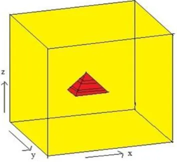
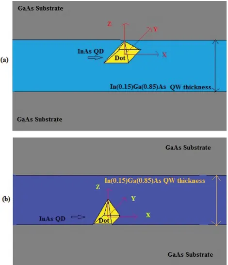
[image:36.612.116.293.456.618.2]directions, 𝑥, 𝑦, and 𝑧, while the thickness of the wetting layer is 0.5 nm. The shape of the QD and the orientation of the QD in the substrate layer are shown schematically in Fig. 2.2.1.1.
FIG. 2.2.1.1 Shape and position of pyramidal quantum dot InxGa1-xAs. Substrate is GaAs and is 15 nm thick on all sides. For the
quantum dot of type InxGa1-xAs/GaAs, the InxGa1-xAs is the material of the quantum dot itself and GaAs provide the trapping
22
We describe such QD within k.p model. The corresponding Hamiltonian include the states of one conduction band and three valence bands. To find the eigenenergies and eigenfunctions of k.p Hamiltonian we use Nextnano software package. This package calculates the electronic and optoelectronic properties of semiconductor nanostructures. The geometric and Hamiltonian parameters, used in the simulations of the quantum dots, are shown in Tables 2.2.1.1-2.2.1.3. Tables 2.2.1.1 and 2.2.1.2 list the sizes of the quantum dot system, which include the sizes of the wetting layers, and geometric orientation of the quantum dot, while the Table 2.2.1.3 shows the parameters of 8-band kp Hamiltonian.
TABLE 2.2.1.1 Pyramidal quantum dots dimensions. Base is a square with equal width and length. Height is always 1/3
the base width.
23
TABLE 2.2.1.3. Parameters of the 8x8 kp model. The interpolation equation for all parameters is given by p[x]= p[0](1-x)
+ p[1]x- bow_p × x(1 – x).
To find the intraband optical transitions within the valence band we calculate 20 valence, i.e., hole, states and then find the optical transitions between these states. The optical transitions (absorption) in such system are allowed only at a finite p-doping of the quantum dot system. Such p-doping introduces a finite number of holes into the system. We assume that the hole concentration is low enough, so that each quantum dot is occupied by one hole only. In this case we do no need to take into account interaction between the
holes and at low temperature only the ground state is occupied. Thus only the ground hole state, 𝜓̂0(𝑟⃗), of
the valence band is occupied, where 𝑟⃗ is a 3D coordinate vector.
Then the absorption spectrum is determined by intensities of optical transitions between the ground
state, 𝜓̂0(𝑟⃗), and excited hole states, 𝜓̂𝑓(𝑟⃗). Within the 8 band k.p model, each wavefunction, 𝜓̂𝑖(𝑟⃗), has
8 components, 𝜓̂𝑖(𝑟⃗) = (𝜓𝑖,1, … , 𝜓𝑖,8), where the components determine the expansion coefficients in the
original basis of the Bloch wavefunctions, 𝑢𝑘(𝑟⃗), where 𝑘 = 1 … 8. Then the wavefunction of a hole in the 8 band k.p model has the following form
Ψ𝑖(𝑟⃗) = ∑8𝑘=1𝜓𝑖,𝑘(𝑟⃗) 𝑢𝑘(𝑟⃗), (2.2.1.1)
With numerically calculated hole wavefunctions, we can find the intensity of optical transition, i.e.
24
for x and z polarized light, respectively. Here 𝑧-direction is the growth direction. The frequency
corresponding to such transition is 𝜔𝑓 = (𝐸𝑓− 𝐸0)/ℏ. Equations (2.2.1.2) and (2.2.1.3) determine the
discrete optical absorption spectra. Below for each absorption peak we introduce the finite Gaussian broadening with the width of 3 meV. The absorption spectra is also characterized by the total intensity
𝐼(𝑠)= ∑ 𝐼 𝑓
(𝑠)
𝑓 , 𝑠 = 𝑥, 𝑧, the first moment, 𝜔𝑎𝑣 (𝑠)
= ∑ 𝜔𝑓𝐼𝑓 (𝑠)/𝐼(𝑠)
𝑓 , 𝑠 = 𝑥, 𝑧 and the second moment 𝑤 =
√∑(𝜔𝑓−𝜔𝑎𝑣 (𝑠)
)2𝐼𝑓(𝑠)
𝐼(𝑠) .
2.2.2 Results and Discussion
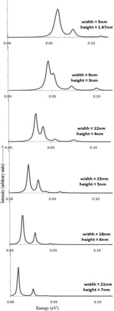
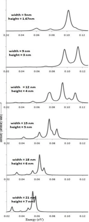
The intraband absorption spectra of the p-doped InxGa1-xAs/GaAs QD are shown in Figs. 2.2.2.1 and 2.2.2.2 for x-polarized light and two different In contents: x =1.0, i.e., InAs/GaAs QD (Fig. 2.2.2.1) and x = 0.7, i.e., In0.7Ga0.3As/GaAs QD (Fig. 2.2.2.2). The results are shown for different sizes of the pyramidal QDs. The properties of two main peaks in the absorption spectra of x-polarized light are summarized in Tables 2.2.2.1 and 2.2.2.2. We observe that the structures of the optical spectra have weak dependence on x (composition of the QD). The composition of the QD mainly determines the energy scale, i.e., the positions of the peaks in the absorption spectra of x-polarized light. The absorption spectra of z-polarized light (for “In” content x = 0.7 and 1.0), which is shown in Figs. 2.2.2.3 and 2.2.2.4, have different behavior. Similar to x-polarized light, the spectra of z-polarized light are red shifted with increasing size of the dot. In Fig. 2.2.2.5, we show the ratio of the intensities of absorption peaks, Ix/Iz,
𝐼𝑓(𝑥)(𝜔𝑓) = |∫ 𝑑𝑟⃗ Ψ0∗(𝑟⃗) 𝑥 Ψ𝑓(𝑟⃗)| 2
, (2.2.1.2)
𝐼𝑓(𝑧)(𝜔𝑓) = |∫ 𝑑𝑟⃗ Ψ0∗(𝑟⃗) 𝑧 Ψ𝑓(𝑟⃗)| 2
25
where for x- and z-polarized light, we consider only the absorption peaks with the highest intensities. The results are shown for QDs with In content x = 0.5, 0.7, and 1.0.
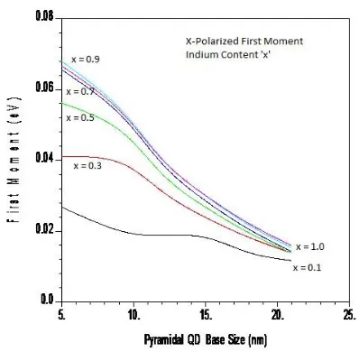
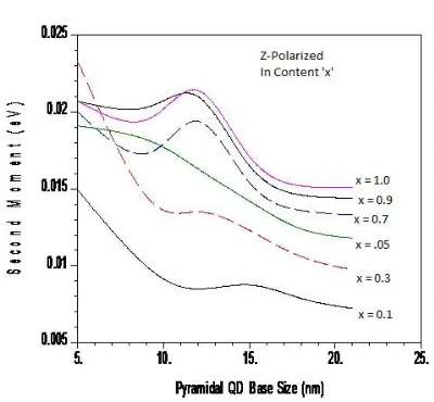
In Figs. 2.2.2.6 and 2.2.2.7, the first moment of the absorption spectra of p-doped QD is shown as a function of size of QD for different “In” content. The results are shown for both x- and z-polarized light. Figures 2.2.2.8 and 2.2.2.9 give, respectively, the second moment of the corresponding absorption spectra of x- and z-polarized incident light. For large sizes of the quantum dots, > 10 nm, the first moments of the absorption spectra have weak dependence on the “In” content of the Inx Ga 1-x As/GaAs quantum dot. The photoresponse to z-polarized light is at higher frequency than the photoresponse to x-polarized light. For sizes 12 nm and above, we can see a monotonic decrease in the second moment for all the values of “In” content “x.” We can observe that the energy of the second moment of x-polarized and z-polarized is about
26
FIG. 2.2.2.1 X-polarized optical transition intensities of
InxGa1-xAs pyramidal quantum dots for base widths 5nm to
21nm. Height=width/3. Indium content is x = 0.7.
FIG. 2.2.2.2 X-polarized optical transition intensities of
InxGa1-xAs pyramidal quantum dots for base widths 5nm to
[image:41.612.76.271.83.613.2]27
TABLE 2.2.2.1 First intensity peak positions for InxGa1-xAs pyramidal QDs with different sizes and with different “indium”
content. Sizes are in “nm” and position of the peak at energy in “eV.”
TABLE 2.2.2.2 Second intensity peak positions for InxGa1-xAs pyramidal QDs with different sizes and with different “Indium”
content. Sizes are in “nm” and position of the peak at energy in “eV.”
The intraband absorption spectra of the p-doped InxGa1-xAs/GaAs quantum dot are shown in Figs. 2.2.2.1 and 2.2.2.2 for x-polarized light and two different In contents: x = 1, i.e., InAs/GaAs quantum dot (Fig. 2.2.2.2) and x = 0.7, i.e., In0.7Ga0..3As/GaAs quantum dot (Fig. 2.2.2.1). The results are shown for different sizes of pyramidal QDs. In both cases, x = 1 and x = 0.7, we can clearly see the general
tendency: with increasing the size of the dot, the absorption spectra are red-shifted. This is a property of a single particle absorption spectra and it follows directly from the general properties of the energy levels in QDs: with increasing the size of the dot, the energy separation between the levels decreases. The structure of the absorption spectra also depends on the size of the dot. For small sizes, b ≈ 5 nm, and for large sizes,
28
dependence on x . The composition of the QD (the value of x) mainly determines the energy scale, i.e., the positions of the peaks in the absorption spectra of x-polarized light. The properties of the two main peaks in the absorption spectra of x-polarized light are summarized in Tables 2.2.2.1 and 2.2.2.2. We can see that the highest intensity peak is at almost the same frequency for the quantum dots (with In content x = 0.7; x = 0.9, and x = 1). The second highest intensity peak occurs at a lower frequency for x = 0.7 than for x = 1 and x= 0.9 quantum dots. For all sizes excepting 5 nm quantum dot with “In” content x
= 0.7, 0.5, and 1.0, the higher intensity absorption peak has the lower frequency than the low intensity peak.
The absorption spectra of z-polarized light (for “In” content x = 0.7 and 1.0), which is shown in Figs. 2.2.2.3 and 2.2.2.4, have different behavior. Although similar to x-polarized light, the spectra of z-polarized light are red-shifted with increasing the size of the dot, the structure of the absorption spectra of z-polarized light is different from the one of x-polarized light. The absorption peak positions and relative intensities of the peaks strongly depend now on the composition of the InxGa1-xAs/GaAs quantum dot, i.e., on the value of x. This is more clearly visible at intermediates sizes of the quantum dots. For example, at the base width of b = 12 nm, for the quantum dot with x = 0.7 (Fig. 2.2.2.3), the
high-intensity absorption peak is at intermediate frequency, while for the quantum dot with x =1 (Fig. 2.2.2.4), the high-intensity peak is at low frequency. At intermediate QD sizes, the absorption spectra have many peaks with comparable intensities. Results obtained here are comparable to the results obtained by Ref. 20 in which it was reported that “mid-infrared absorption between confined levels of undoped InAs/GaAs
self-organized QDs has shown intraband absorption in the range 90-250 meV along the growth direction (z).” Hole energies presented in this paper are found to be in qualitative agreement with the theoretical
29
FIG. 2.2.2.3. Z-polarized optical transition intensities of InxGa1-xAs pyramidal quantum dots for base widths 5 nm to 21 nm. Indium content is x= 0.7
[image:44.612.81.270.74.544.2]30
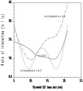
FIG. 2.2.2.5. Plot of X-polarized intensity to Z-polarized intensity as a function of base size (nm) of the InxGa1_xAs pyramidal
quantum dots. Ix to Iz increased from about 5 to 40 as the base size of the pyramid increased from 5 nm to 21 nm.
In addition to different structures of the absorption spectra, the x- and z-polarized lights have quite different intensities. Namely, the intensity of the absorption peak of x-polarized light is larger than the intensity of the absorption peak of z-polarized light. In Fig. 2.2.2.5, we show the ratio of the intensities of absorption peaks, Ix/Iz, for x- and z-polarized light. We consider only the absorption peaks with the highest intensities with the QDs having In content x = 0.5, 0.7, and 1.0. These data show that the
31
decreases with decreasing the In content. The strength of the suppression of the ratio of intensities with decreasing In content, x, depends on the size of the dot. For example, for QD with size 16 nm, the ratio of intensities decreases by a factor of 2 (see Fig. 2.2.2.5) when the In content is changed from x = 1.0 to x = 0.7, while for QD with size 12 nm, the ratio of intensities does not depend on the In content (for the values of x= 0.5, 0.7, and 1.0). Therefore, from the data of Fig. 2.2.2.5, we can conclude that the p-doped QD mainly absorbs the x-polarized light.
In Figs. 2.2.2.6 and 2.2.2.7, respectively, we show, for the x-polarized and z-polarized incident light, the first moment of the absorption spectra as a function of the size of the QD for different “In” content. Except for z-polarized light and In0.7 Ga0.3 As/GaAs QD, the first moment of the spectrum is red-shifted with increasing the size of the dot. Therefore, the first moment monotonically decreases with
increasing the size of the dot. For the absorption spectrum of z-polarized light and In0.7
[image:46.612.324.523.248.443.2]Ga0.3As/GaAs QD, the first moment as a function of the dot size has a maximum at dot size ≈10 nm.
FIG. 2.2.2.6. Plot of first moment (eV) of X-polarization as
a function of base size (nm) of the InxGa1-xAs pyramidal
quantum dots. First moment of X-polarization is below that
of Z-polarization (Fig. 2.2.2.7) by about 0.06 eV and the
32
FIG. 2.2.2.7. Plot of first moment (eV) of Z-polarization as
a function of base size (nm) of the InxGa1-xAs pyramidal
quantum dots. First moment of X-polarization is below that
of Z-polarization by about 0.06 eV and the difference is
maintained as the size increased.
FIG. 2.2.2.8. Plot of second moment (eV) of X-.
FIG. 2.2.2.9. Plot of second moment (eV) of Z-polarization
as a function of base size (nm) of the InxGa1-xAs pyramidal
quantum dots.
polarization as a function of base size (nm) of the
InxGa1-xAs pyramidal quantum dots
[image:47.612.324.524.319.504.2]33
can conclude (Figs. 2.2.2.6 and 2.2.2.7) that the frequency of absorbed z-polarized light is larger than the frequency of absorbed x-polarized light by ≈ 50 meV. Therefore, the photoresponse to the z-polarized light is at higher frequency than the photoresponse to the x-polarized light. Figs. 2.2.2.8 and 2.2.2.9 give, respectively, the second moments of the absorption spectra of x-polarized and z-polarized incident light. For the QD sizes 12 nm and above, we can see a monotonic decrease in the second moment for all the values of “In” content “x.” We observe that the values of the second moment of x-polarized and z-polarized absorption spectra are about the same for a given “In” content or “x” value.
Summarizing the analysis of optical spectra of p-doped InxGa1-xAs/GaAs we can conclude that optical spectra is sensitive to the size of QD and In content. The QD is sensitive to both x- and z-polarized light. For a given size of the quantum dot, the absorption frequency of z-polarized light is higher than the absorption frequency of x-polarized light by ≈ 50 meV. With increasing the size of the quantum dot, the absorption spectra is shifted to lower energies, which allows tuning the absorption frequency of the quantum dot system. For x-polarized light, the corresponding wavelength of absorbed light changes from 21.4 μm to 250 μm as the size of the base of the quantum dot increases from 5 nm to 21 nm. For
z-polarized light, the corresponding wavelength increases from 11.8 μm to 19.8 μm with increasing the size of the dot from 5 nm to 21 nm. The frequency of the light, absorbed by InxGa1-xAs/GaAs quantum dot, has weak dependence on In content of the quantum dot, except for the quantum dot of a small size, < 10 nm.
2.3 Optical properties of dot-in-a-well systems
2.3.1 Model and Main Equation
34
with a square base. The four sides of pyramidal QD are oriented in the (011), (0-11), (101) and (-101) directions, respectively. Such QD is characterized by two geometric parameters: the size of the base, 𝑏, of
the dot, which is the size of corresponding square; and the height, ℎ of the dot. In all calculations below we fixed the ratio ℎ/𝑏 assuming that ℎ = 𝑏/3. Under this condition, the size of the quantum dot is determined
by only one parameter, e.g. the size of the base of the dot, 𝑏, which we call below just the size of the quantum dot. In our calculations, we vary both the size of QD and the thickness of QW. The thickness of
substrate above and below quantum well is 15 nm in all three directions, 𝑥, 𝑦, and 𝑧. The shape and position of the QD and orientation of the QD in the quantum well and substrate layer are shown schematically in Fig. 2.3.1.1a and Fig. 2.3.1.1b. In all calculations below we assumed that In content is 0.15 , i.e., we
consider InAs/In0.15Ga0.85As/GaAs DWELL systems.
To find energy spectrum and corresponding wave functions of DWELL system we employ one band (conduction band) effective mass model. To do this we use NEXTNANO software package [80]. This package calculates the electronic and optoelectronic properties of semiconductor nanostructures. The geometric parameters, used in simulations of quantum dots and quantum wells, are shown in Tables 2.3.1.1 and 2.3.1.2, where the sizes of DWELL system, geometric orientation of the quantum dot, and parameters of the model are listed. The Hamiltonian of this model is given by,
𝐻 = 𝑝⃗ 1
35
FIG. 2.3.1.1
Schematic illustration of the dot-in-a-well system. The quantum dot (InAs) is at the
36
TABLE 2.3.1.1Dimensions of the quantum well and the pyramidal quantum dot, which are used in our calculations. The dot base is a square and we define the dot size as the length, b, of the side of the square. The dot height is 1/3 of the dot size, h = b/3.
TABLE 2.3.1.2. Parameters of the numerical model of DWELL system.
To find the intraband optical transitions within the conduction band of the system, we calculate 20 eigenstates of the system and then find the optical matrix elements between these states. The optical transitions (absorption) in such system are allowed only at a finite n-doping of the quantum dot system. Such n-doping introduces a finite number of electrons into the quantum dot. We assume that the electron concentration is low enough, so that each quantum dot is occupied by one electron only. In this case we do no need to take into account inter-electron interactions, and at low temperature, only the ground electron state, Ψ0(𝑟⃗), of the system is occupied, where 𝑟⃗ is 3D coordinate vector. Then the intensity of optical
transition, i.e. intensity of optical absorption, from the initial ground state, Ψ0(𝑟⃗), with energy 𝐸0 to the
37
for x and z polarized light, respectively. Here 𝑧-direction is the growth direction. The frequency
corresponding to such transition is 𝜔𝑓 = (𝐸𝑓− 𝐸0)/ℏ. Equations (2.3.1.2) and (2.3.1.3) determine the
discrete optical absorption spectra. Below, for each absorption peak we introduce the finite Gaussian
broadening with the width of 3 meV. The absorption spectra is also characterized by total intensity 𝐼(𝑠)=
∑ 𝐼𝑓 𝑓(𝑠), 𝑠 = 𝑥, 𝑧, the first moment, 𝜔𝑎𝑣 (𝑠)
= ∑ 𝜔𝑓𝐼𝑓 (𝑠)/𝐼(𝑠)
𝑓 , 𝑠 = 𝑥, 𝑧 and the second moment 𝑤(𝑠)=
√∑(𝜔𝑓−𝜔𝑎𝑣(𝑠)) 2
𝐼𝑓(𝑠)
𝐼(𝑠)
2.3.2 Results and Discussion
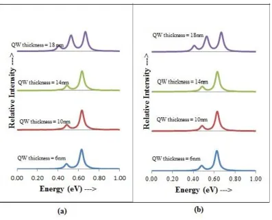
The absorption spectra of n-doped InAs/In0.15Ga0.85As/GaAs QWELL system with the dot size of 5 nm are shown in Fig. 2.3.2.1 for x-polarized light and for two different positions of the QD: at the bottom of the QW (Fig. 2.3.2.1(a)) and at the top of the QW (Fig. 2.3.2.1(b)). The results are shown for different thicknesses of the quantum well, which is varied in the range between 6 nm and 18 nm. The general tendency is clearly visible from the data shown in Fig. 2.3.2.1. Namely, the absorption spectra have very weak dependence on the position of the QD, i.e. the spectra shown in the left panel are almost identical to the corresponding spectra shown in the right panel. Another feature of the optical spectra shown in Fig. 2.3.2.1 is a weak dependence of the spectra on the thickness of the QW, hwell. For the thickness of the well less than 18 nm the spectrum consists of two main peaks separated by ≈ 100 meV. The positions of the
𝐼𝑓(𝑥)(𝜔𝑓) = |∫ 𝑑𝑟⃗ Ψ0∗(𝑟⃗) 𝑥 Ψ𝑓(𝑟⃗)| 2
, (2.3.1.2)
𝐼𝑓(𝑧)(𝜔𝑓) = |∫ 𝑑𝑟⃗ Ψ0∗(𝑟⃗) 𝑧 Ψ𝑓(𝑟⃗)| 2
38
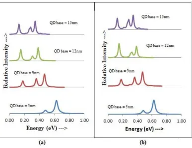
[image:53.612.75.472.295.616.2]peaks and their relative intensities do not depend on the QW thickness. The dependence on the well thickness occurs at larger values of hwell ≥ 18 nm. For the QW with the thickness of 18 nm, the optical spectrum has three well-separated peaks, which is different from small thickness behavior. Weak dependence of the optical spectra of DWELL system on the QW thickness was also reported in Ref. [89]. The data shown in Fig. 2.3.2.1 illustrates that the optical spectra have weak dependence on the position of the QD within the well. Although the results of Fig. 2.3.2.1 corresponds to a given size of the QD and the x-polarized light, the weak dependence of the spectra on hwell is also observed for other sizes of the QD and for z-polarized light. Therefore below (see Fig. 2.3.2.2) we show the absorption spectra of DWELL system only for one position of the dot in the well, e.g., for the QD at the bottom of the well.
FIG. 2.3.2.1 Absorption spectra for x-polarized light. The size of the quantum dot is 5 nm. The dot is (a) at the bottom and (b) at
the top of the quantum well.
39
FIG. 2.3.2.2. Absorption spectra of DWELL system for (a) x-polarized light and (b) z-polarized light. The thickness of the
quantum well is 6 nm. The dot is at the bottom of the well.
The characteristics of two main peaks (see Fig. 2.3.2.1) in the absorption spectra of x-polarized light are summarized in Table 2.3.2.1. To compare the actual position of the absorption peaks for x- and z-polarized light, we summarize in Table 2.3.2.2 the properties of two main peaks of the absorption spectra of z-polarized light (the second peak has much smaller intensity than the main peak). The main peak for z-polarized light corresponds to optical transitions from the ground state of the dot to either the states of the substrate or the states of the QW. Although the optical spectra show weak sensitivity to the QW size, they are sensitive to the size of the QD. The dependence of the absorption spectra on the dot size is
40
absorption spectra in QD systems: with increasing the size of the dot the energy separation between the levels decreases, which results in red shifting of the absorption spectra.
For x-polarized light [see Fig. 2.3.2.2(a)], the shape of the absorption spectra strongly depends on the size of the dot. For the dot of small size, b∼ 5 nm, there is one main absorption peak. With increasing the size of the dot, more peaks appear in the absorption spectra and the spectra show multipeak structure. Redistribution of the absorption intensities between the peaks has non-monotonic dependence on the dot size. The characteristics of two main peaks in the absorption spectra of x-polarized light are summarized in Table 2.3.2.1. The frequency of the optical transition is red shifted as the size of the dot increases and, as it was mentioned before, the frequency is independent on the size of the quantum well for the same dot size. For the quantum dot of small size, b = 5 nm, the optical transitions occur between the states of the QD and substrate, while at larger dot size, b = 9 and 12 nm, the transitions occur between the states of the QD and the QW.
41
TABLE 2.3.2.1 Optical transitions corresponding to two main peaks of the absorption spectra are listed for x-polarized
light.
TABLE 2.3.2.2 Optical transitions corresponding to two main peaks of the absorption spectra are listed for z-polarized