Hewlett-Packard
98041A Disc Interface
Installation and Service Manual
-HEWLET~". PACKARD
Warranty Statement
Hewlett-Packard products are warranted against defects in materials and workmanship. For Hewlett-Packard Desktop Computer Division products sold in the U.S.A. and Canada, tllis warranty applies for ninety (90) days from date of delivery. * Hewlett-Packard will, at its option, repair or replace equipment which proves to be defective during the warranty period. This warranty includes labor, parts. and surface travel costs, if any. Equipment returned to Hewlett-Packard for repair must be shipped freight prepaid. Repairs necessitated by misuse of the equipment, or by hardware, software, or interfacing not provided by Hewlett-Packard are not covered by this warranty.
NO OTHER WARRANTY IS EXPFlESSED OR IMPLIED, INCLUDING, BUT NOT LIMITED TO, THE IMPLIED WARRANTIES OF MERCHANTABILITY AND FITNESS FOR A PARTICULAR PURPOSE. HEWLETI-PACKARD SHALL NOT BE LIABLE FOR CO \JSEQUENTIAL DAMAGES.
* For other countries, contact your local Sales and Service Office to
98041A Disc Interface
Installation and Service Manual
Hewlett-Packard Desktop Computer Division
3404 East Harmony Road, Fort Collins, Colorado 80525 (For World-wide Sales and Service Offices see back of manual.)
iii
Chapter 1: General Inforolation
Introduction ... 1
Equipment Supplied ... 1
Specifications ... 2
Technical Specifications ... 2
Chapter 2: Installation Power Requirements ... 3
Grounding Requirements ... . ... 3
Fuses ... 4
Power Cords ... 4
Installing the Disc Interface ... 5
Interface Select Code ... 6
HP-IB Capabilities ... 7
Connecting Mass Storage Controllers ... 7
Interconnecting Cables ... 7
Cable Length Restrictions ... 8
ROM Requirements ... 9
Mass Storage Unit Installation ... 9
Rack Mounting ... . . . 9
Chapter 3: Theory of Operation and Service Disc Interface General Description ... 11
System Operation Overview ... 12
Interface Logic Levels ... 12
Interface Card Operation ... 12
The Al I/O Control Board ... 12
The A2 Data Logic Board ... 13
Central Data Unit Operation ... 13
The A3 Support Board ... 14
The A4 HP-IB Board ... 14
The I/O Regis tE~rs ... 14
The PHI Chip. . . 15
The FIFO Buffer ... . . . .. 1 7 The PHI Access Control ... 17
The Byte Packing Control ... 18
iv
The Interrupt Request Logic ... 18
The HP-IB Transceivers ... . 18
The AS HP-IB Connector Board .. . 18
The A6 Power Supply Board ... 19
Interface Block Diagram ... 21
Sequential Operation Description ... 23
Non-DMA Output Operation ... 23
Non-DMA Input Operation ... 23
Computer DMA Output Operation ... 24
Computer DMA Input Operation ... 26
Additional Theory of Operation ... 29
The PHI Access and Byte Packing Control State Machines ... 29
Byte Packing Control State Diagram ... 31
PHI Access Control State Diagram. . ... 33
Servicing the Disc Interface ... 35
Disc Interface Disassembly Procedur es ... 35
Al and A2 Assembly Access ... 36
A3 thru A 7 Assembly Access ... 37
Removing the A4 HP-IB Board ... 38
Removing the A6 Power Supply Board ... 38
Removing the A3 Support Boare ... 40
Removir:tg the AS HP-IB Connector Board ... 40
Removing the A 7 I/O Cable As~embly ... 42
Replacing the PHI Chip (A4U 1) ... . ... 44
Adjusting the PHI Internal Timing. . . . .. . ... 45
Procedure ... . ... 45
Glossary of Line and Signal Name Abbreviations ... 48
Al I/O Control Board Al Replaceable Parts. . . .. . ... 51
A 1 Component Locator. . . .. . ... 51
A 1 Schematic Diagram. . . .. ... 51
A2 Data Logic Board A2 Replaceable Parts . . . .. . ... 53
A2 Component Locator ... . A2 Schematic Diagram ... . A3 Support Board A3 Replaceable Parts ... . A3 Component Locator ... . A3 Schematic Diagram ... . ... 53
... 53
. ... 55
. ... 55
v
A4 HP-IB Board
A4 Replaceable Parts ... 57
A4 Component Locator ... 58
A4 Schematics Diagram Part 1 ... 59
A4 Replaceable Parts ... 61
A4 Component Locator ... 62
A4 Schematic Diagram Part 2 ... 63
A4 Replaceable Parts ... 65
A4 Component Locator ... 66
A4 Schematic Diagram Part 3 ... 67
AS HP-IB Connector Board AS Replaceable Parts ... 69
A6 Power Supply Board A6 Replaceable Parts ... 71
A6 Component Locator ... 71
A6 Schematic Diagram ... 71
A 7 I/O Cable Assembly A 7 Replaceable Parts ... 73
A 7 Connector Wiring Diagrams ... 73
Chassis and Case Components ... 75
Appendix ... 77
13037 Disc Controller Service Notes ... 78
Sales and Service Offices ... 82
Figures Line Voltage Switches ... 3
Power Cords ... 5
HP 98041A Disc InterfacE~ ... 6
Interface Select Code Swilch ... 6
Standard HP-IB Cables ... 7
Example System ConfigUirations ... 8
Basic Control Machine Structure ... 29
Structure of the Controller Circuitry ... 30
Interface Card Disassembly ... 36
A3 thru A 7 Assembly Access ... 37
Removing the A4 HP-IB Board · ... 38
Removing the A6 Power Supply Board ... 39
Removing the A3 Support Board ... 40
Removing the A5 HP-IB Connector Board ... 41
vi
Removing and Replacing the PHI Chip ... 44 Adjusting the PHI Chip . . . .. ... . . . . ... 45
Service Kit Component Locations .... 47
Tables
General Information 1
Chapter
1
General Information
Introduction
The HP 98041A Disc Interface connects an HP System 45 Desktop Computer to a wide variety of high speed, mass storage peripherals.
This manual provides you with 98041A equipment specifications, installation procedures and general mass storage system information. In addition, service information including the theory of operation for the interface, replaceable parts lists, component locators and schematics is provided.
I:quipment Supplied
The following items are supplied with each disc interface.
Description Quantity Part Number
Installation Manual 1 98041-90000
Power Cord 1 8120-1378*
Spare Fuse
.75A,250V,NB 1 2110-0033
1.5A,250V,NB 1 2110-0043
Rack Mount Hardware
Screws 4 2680-0103
Washer 4 3050-0257
2 General Information
Specifications
The following specifications are for the 98041A Disc Interface only. Refer to the Installation and Service Manuals for each mass storage unit in the system for its specifications and operating limitations.
Technical Specifications
Environme ntal
Operating Temp: 00 C to 550 C Non-Operating Temp: -400
C to 650 C Relative Humidity: 0 to 95% at 250 to 400
C (770 to 1040 F) thout condensation
Physical Dimensions
Power Requirements
Installation 3
Chapter
2
Installation
The disc interface operates from power line voltages of 100, 120,220 or 240 volts ac. The range of operation is within +5% and -10% of each nominal voltage. Two switches on the disc interface back panel permit selection of anyone of the four nominal volta~ges (see Figure 2:.11. The line frequency must be within 48 to 66 Hz. The disc interface requires a maximum of 120 voltamps.
CAUTION
THE DISC INTERFACE MAY BE DAMAGED IF THE LINE VOLTAGE SWITCH SETTINGS ARE INCORRECT. CHECK THE SWITCH SETTINGS BEFORE APPLYING POWER.
IL~m
iL'AlE IL'Aill
I?O IQOiL'A~
9
IQO\
@~
(~
a5
@~
@
I~
L~~
L750mA J L750mA J L750mA J
IOO~ts 120 Volts 220 Volts 240 Volts
(I.5A Fu .. ) O.5A Fuse) (.75A FUM) . (~A Fuse)
Figure 2·1: Line Voltage Switches
Grounding Requirements
4 installation
Fuses
The disc interface must be fitted with a 1.5 amp normal blow fuse for 100-120 volt operation or a .75 amp normal blow fuse for 220-240 volt operation. Fuse part numbers are listed in the Equipment Supplied Table in Chapter 1.
WARNING
BEFORE CHANGING THE FUSE, BE SURE THAT THE DISC INTERFACE IS DISCONNECTED FROM ANY POWER SOURCE.
To remove a fuse, press in on the cap of the fuse holder and twist the cap in the direction indicated by the arrow on the cap. Pull the cap free and remove the fuse.
To install a fuse, place either end of the fuse into the pocket in the cap and reinstall the cap by preSSing in on the cap and twisting it in the opposite direction from the arrow.
Always be sure that the correct fuse is used. The wrong fuse could result in damage to the disc interface if a malfunction or unusual line voltage occurs.
Power Cords
Power cords supplied by HP will have polarities matched to the power-input socket on the equipment, as shown below:
• L = Line or Active Conductor (also called 'live' or 'hot')
• N
=
Neutral or Identified ConductorWARNING
IF IT IS NECESSAHY TO REPLACE THE POWER CORD, THE REPLACE-MENT CORD MUST HAVE THE SAME POLARITY AS THE ORIGINAL, OTHERWISE A SAFETY HAZARD FROM ELECTRICAL SHOCK TO PER-SONNEL, WHICH COULD RESULT IN INJURY OR DEATH, MIGHT EXIST. IN ADDITION, THE EQUIPMENT COULD BE SEVERELY DAM-AGED IF EVEN A RELATIVELY MINOR INTERNAL FAILURE OCCUR-RED.
Installation
5
Power cords with different plugs ar,e available for the equipment; the part number of each cord is shown in Figure 2-2. Each plug has a ground connector. The cord packaged with the equipment depends upon where the equipment is to be delivered.
~~~
"/~~L'\i ~
L [
812001371 ' 8120.-2
~~(e
\ ~ ,. / ~N
L [
812().2104
~
CALCULATORPOMR·INP\JT SOCKET
1 UL and CSA approved for use in the United States of America and Canada with equipment set
for either 100 or 120 Vat; operation.
2UL and CSA approved for use in the United Stat . . of America and Canada with equipment set for either 200 or 240 Vac operation.
Figure 2-2: Power Cords
Installing the Disc Interface
[image:13.612.208.482.343.477.2]6 Installation
[image:14.612.213.346.563.703.2]Plug the disc interface I/O card into anyone of the I/O slots in the back of the computer. The mass storage controller unit (or units) connect to the HP-IB connector located on the back of the 98041A central data unit. Figure 2-3 shows a 98041A Disc Interface connected to a System 45 computer and an HP 13037B Disc Controller with a 7906A Disc Drive.
Figue 2-3: Connecting the HP 98041A Disc Interface
Interface Select Code
The 98041A is preset at the factory to select code 12. Select code 12 is the computer's default select code whenever a MASS STORAGE IS statement is executed specifying a mass storage unit that is connected to a 98041. Refer to "Mass Storage Operations" in the computer Operating and Programming manual for details concerning mass storage program statements.
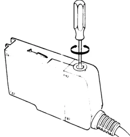
If you need to change the select code setting on the disc interface, it can be set to any value from 1 to 12. The select code switch is accessible through a small hole on the top of the I/O card case (Figure 2-4). To change the setting, rotate the switch using a small screwdriver until the small arrow on the switch points to the desired select code number.
Installation
7
HP-IB Capabilities
Although the 98041A Disc Interface is a valid implementation of the HP-IB IEEE standard 488-1975, the special use of specific secondary commands that are unique to specific mass storage controllers does not permit using other HP-IB peripherals (such as Plotters, Printers, Tape Drives, etc.) with the 98041. All other HP-IB peripherals should be connected to the computer via a 98034A HP-IB Interface.
NOTE
Although both interfaces use the same type of connector, only properly designed mass stora!:Je controllers should be connected to the 98041A Disc Interface and general HP-IB peripherls should be connected to the 98034A HP-IB Interface.
Refer to Supplement A to this manual for a complete list of the HP mass storage units that are compatible with the 98041A.
Connecting Mass Storage Controllers
A maximum of two mass storage controller units may be connected to an HP 98041A Disc Interface. These controllers can be separate units that can each control several disc drives, or a controller and a disc drive built into one unit.
Interconnecting Cables
Standard HP-IB cables are used to connect the mass storage controller units in your system to the disc interface. Listed in Figure 2-5 are the accessory numbers of the various cables that are available.
Length
1 metre
2 metres
4 metres
Accessory Number
10631A 106318 10631C
8
InstallationCable Length Restrictions
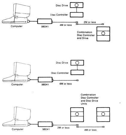
The total cable length connecting the disc interface with the mass storage controllers connected to it must be less than or equal to 6 metres. The cable may be distributed between the disc interface and the mass storage controllers in any manner that is practical, as long as the total length does not exceed 6 metres. This cable length restriction does not, however, include any cables used to connect a controller to its various disc drives. Refer to the installation manual for each disc drive and disc controller unit in your system for information concerning the cables and connections between those units. Figure 2-6 shows example system configurations using the allowable cable length of 6 metres between the disc interface and various disc controller units.
Computer
Computer
Computer
98041
98041
98041
Disc Drive
~
Disc Controller
0
4M or less
2M or less o
Combination Disc Controller and Drive
DlscDrive
~
Disc Controller
0
6M or less
2M or less c
Combination Disc Controller and Disc Drive Units
[image:16.615.107.528.262.711.2]4M or less
Figure 2-6: Examlple System Configurations
o
Installation 9
ROM Requirements
The disc interface requires that the Mass Storage ROM be properly installed in the computer to provide the statements necessary to store data on the mass storage units. Refer to the Mass Storage Techniques Manual for ROM installation and programming information.
Mass Storage Unit Installation
The installation procedure for the various mass storage units that are compatible with the disc interface are contained in their respective Installation and Service Manuals. Refer to Supplement A for a listing of the manual part number of each compatible unit.
Rack Mounting
Rack Mounting
Theory of Operation 11
Chapter
3
Theory of Operation and Service
Disc Interface General Description
The 98041A Disc Interface consists of two physical components as shown in the typical system block diagram below.
• An Interfac~~ card and cable
98041
• A Central Data Unit
DiSC~
Drive
Disc Controller
CI
The Interface card connects to any of the computer's I/O slots. The central data unit is attached to the interface card's 3 metre cable. Up to two disc controllers can be connected to the central data unit via standard HP-IB cables with a total cable length of 6 metres or less. Each disc controller is then connected to the disc drives according to its specific installation requirements.
Diagnostic Test Program
A Diagnostic Test Program is availia.ble on the 98041A Test Cartridge (P /N 98041-90010) for use with the System 45 Desktop Computer. This test can be used to verify the .operation of the disc interface and the mass
I storage units in the system.
The 98041A Disc Interface Diagnostic Program Manual (P /N 98041-90031) contains the necessary informa-tion for loading and running the dias!nostic test.
12
Theory of OperationSystem Operation Overview
The general function of the disc interface is to transfe" data to and from various mass storage devices consisting of disc controllers and disc drives. The disc interfac 2 converts the computer's mass storage instructions into
HP-IB disc controller commands. Additionally, the interface converts the computer's 16-bit data into two 8-bit bytes that are useable by the discs and also compensates for the input/ output speed differences between the computer and the disc controllers.
A block diagram of the disc interface is on page . Unfold the diagram for reference as you read this section. Following the block diagram is an operational explanation of the various components of the disc interface. Complete schematic diagrams, component locators and replaceable parts lists are given for each assembly. A glossary of signal abbreviations is included with the schematics.
Interface Logic Levels
The Disc Interface uses TTL logic levels. Throughout this manual, all logic levels and signal levels will be referred to as either "high" (~ 2V) or 'low' (~ 0.8V)
Theory of the Interface Card Operation
The interface card contains two printed circuit assemblies: the Al I/O Control Board and the A2 Data Logic Board. These assemblies consist of driver, receiver and terminator components for the 16 data lines, 5 status lines and 6 control lines as well as part of the I/O control logic.
The Al I/O Control Board
The I/O control board assembly (P /N 98041-66501) contains the drivers for the 6 control lines. These lines and their functions are defined as follows.
The ICI and IC2 lines from the computer's I/O control specify the type of I/O operation that is to be executed. The following table shows the line level for each operation
-IC2 ICI Operation
high high DMA Data transfer
low high DMA Data transfer last word.
low low Non-DMA data transfer
high low Input status information or send control information.
Theory of Operation
13
The IOS8 line carries the handshake strobe pulse from the computer I/O control. The strobe driver is enabled
only if the select code on lines PAO thru PA3 specify a value that is the same as the value set on the select code switch (S 1). This line leaves the A 1 board as the GQIOSB line.
The DOUT line specifies the transfer direction for the operation being executed by the computer (either input or output). The DOUT driver is enabled only when the select code value on lines PAO thru PA3 is the same as the value set on the select code switch (SI). The DOUT line leaves the Al board as the GQDOUT line.
The INT line causes the I/O card to respond to an interrupt poll performed by the computer's I/O control.
The Al board also contains the select code decoding logic and the poll response decoding logic.
The A2 Data Logic Board
The Data Logic assembly (P /N 98041-66502) contains the drivers and receivers for the 16 data lines and the receivers for the 5 disc interface status lines. The status lines are defined as follows.
The GIRQ line sends an interrupt n:!quest signal from the central data unit to the computer I/O control as either a low priority interrupt IRL (for select code settings of 2 thru 7) or a high priority interrupt IRH (for select code settings of 8 thru 12). The GIRQ line also enables the poll response logic to respond to a poll operation conducted by the computer's I/O control.
The GDMAR line is used by the central data unit to request a DMA operation from the computer.
The GSTS line specifies whether or not the central data unit is powered on and whether or not a DMA transfer is enabled.
The
G'Fi:G
line carries the central data unit's part of the non-DMA transfer handshake in response to the GQIOSB pulse from the computer I/O control.The GPOP line indicates that either the central data unit has just powered up (via the GPOPP line from the disc interface power supply) or the computer has just been powered up or reset (via the GINIT line from the computer).
Theory of tile Central Data Unit Operation
14
Theory of OperationThe A3 Support Board
The support board assembly (P IN 98041-66504) c::mtains the components that complement the signal lines
coming from or going to the A 1 and A2 boards. The~e components include receivers and terminators for the 6 control lines, drivers for the 5 status lines, and transceivers and terminators for the 16 bidirectional data lines. This board also receives the +5 Volt, + 12 Volt and ground lines from the A6 power supply assembly. All of the lines are then connected to the A4 HP-IB board.
The A4 HP-IB Board
The HP-IB board assembly (P IN 98041-66507) contains the circuits necessary to convert the computer's
strobed, 16-bit data words into two 8-bit data bytes. This data is transfered into the PHI chip (A4 Ul) using a two wire type handshake with the computer. The PHI chip also transfers the data bytes to and from the selected mass storage controller units using the HP-IB disc ccntroller commands and the HP-IB three wire handshake.
The basic hardware components of the HP-IB board are as follows
• I 10 Registers .PHI Chip
• Sixteen Byte FI FO Buffer
• PHI Access Control State Machine
• Byte Packing Control State Machine
• FIFO Fullness Counter
• DMA Request Logic
• Interrupt Request Logic
.HP-IB Transceivers
The I 10 Registers
There are two types of 1/0 registers on the HP-IB board: the bidirectional 16-bit data registers and the 6-bit instruction register.
Theory of Operation
15
The instruction register is a 6-bit latch that accepts instructions from the computer on data lines 100 0 thru 100 5 when the IC 1 and IC2 lines select an instruction operation. Three bits of the data (laD 5 thru 100 3) form the PHI chip register address and three bits (laD 2 thru 100 0) specify the type of operation to be performed. The bit values for the PHI chip register address and the operation codes are shown next.
Register No. 0105 0104 0103
Reg 0- low low low
Reg 1 - low low high
Reg 2- low high low
Reg 3- low high high
Reg 4- high low low
Reg 5- high low high
Reg 6- high high low
Reg 7- high high high
0103 0101 0100 Type of Operation
high high high Non-DMA write to specified PHI Register high high low Non-DMA read from specified PHI Register
high low high Don't Care
high low low Reset
low high high DMA Output - Computer memory to
disc controller / drive
low high low DMA input - disc controller / drive to computer memory
low low high Don't Care
low low low No-op
The PHI Chip
The PHI chip (A4 U 1) controls the bi-directional tri-state transceivers which send and receive information at speeds compatible with HP-IB disc controllers and drives. The PHI chip sends disc addresses and commands according to the HP-IB disc-controller command protocol. This protocol is a valid implementation of the IEEE Std. 488-1975 but makes special use of some "don't care" states in certain HP-IB messages. This control protocol also utilizes certain secondary address characters as commands that are used to select various disc controller operations.
16 Theory of Operation
The PHI is structured on the computer side of the interface as a group of eight la-bit registers, with various control lines to the Control State Machines and a tv/o wire handshake.
The 3-bit address from the instruction register is used to select the specific PHI register for the operation to be performed. The registers are defined as follows:
Register 0:
Register 1:
Register 2:
Register 3:
Register 4:
Register 5:
Register 6:
Register 7:
Contains the values of 9 ~tatus conditions that are capable of interrupt-ing the computer's I/O. These values are masked by the values in Register 1. If any of the nJ ne status conditions are masked and true, the 10th bit of the register is set true which enables the interrupt request logic.
Contains the mask values for the 9 interrupt status conditions in register O. A true value of 1 for a bit, unmasks or selects the corresponding bit in register a as being capable of initiating an interrupt request.
Used to transfer data to or from the HP-IB side of the system. It is structured as two 8 byte FIFO buffers; an inbound FIFO and an out-bound FIFO.
Contains the values of the non-interrupting status conditions.
Contains the 8 control bits used to set up operational conditions within the PHI chip.
Contains the HP-IB addn~ss of the PHI chip.
Masks the 8 incoming responses to a parallel poll operation conducted by the disc interface to defect service requests from mass storage units in the system.
Normalizes the 8 incominq parallel poll responses from the mass storage units in the system.
NOTE
Theory of Operation 17
Non-DMA I 10 Transfers
The non-DMA 1/0 operations are used to transfer mask, command and status bytes to and from the PHI registers. Each of these operations r<equires two computer I I 0 cycles: one cycle to send the PHI register number and the operation code to th4:! instruction latch and one cycle to transfer the data byte to or from the addressed PHI register.
Typical uses of non-DMA data transfers are sending HP-IB addresses or commands, programming the interrupt mask, obtaining interface status, setting PHI chip control bits, setting up DMA data transfers, and obtaining a parallel poll response.
DMA I/O Transfers
High speed data transfers to and from mass storage devices take place under computer DMA control. The disc interface must be programmed before the DMA transfer occurs. This programming process requires three computer I/O cycles. The first cycle specifies a write operation to PHI register 4. The next cycle sends the proper bit pattern to register 4 to set the DMA FIFO select bit which enables the DMAR line out of the PHI chip. The third I/O cycle specifies either a DMA input or output operation and selects PHI register 2 to transfer the data.
Once these cycles have programmed the interface, the OMA data transfer takes place.
The FIFO Buffer
The FIFO (First-In, First-Out) buffer is used only when a DMA data transfer takes place. This buffer is by passed during all non-DMA operations.
The FIFO transfers data in 8-bit bytes, to and from register 2 of the PHI chip and the I/O data registers. It can hold up to sixteen bytes.
Sixteen bit data is transferred to and from the I/O data registers and the FIFO in two 8-bit bytes, with the most significant byte (lOD8 thru IOD15) tratnsfered first followed by the least significant byte (1000 thru 1007). The FIFO buffer can hold up to sixteen bytes of data to allow for speed variations that may occur between the computer's DMA transfer rate and the: data transfer rate of the disc controller.
The PHI Access Control
This circuit provides the control signals for all data transfers between the PHI chip and either the FIFO buffer or the I I 0 latches. The PHI access control is programmed by data from the instruction latch I decoder that specifies the type of transfer to be performed and the PHI register to be used for the transfer.
18
Theory of OperationThe Byte Packing Control
This circuit controls the packing of bytes into words and the unpacking of words into bytes between the I/O latches and the FIFO buffer during DMA operations. It also controls the DMA request logic. The byte packing control receives its control signals from the PHI access control and the FIFO fullness counter.
A more detailed description of the operation of the PHI Access and the Byte Packing Control machines as well as a state diagram is provided on page 21.
The FIFO Fullness Counter and
The DMA Request Logic
The fullness of the FIFO buffer is monitored by the r=IFO fullness counter. This circuit monitors both the PHI access control and the byte packing control to prev"mt either an overflow or underflow of data during DMA transfers.
During DMA output transfers, the fullness counter prevents data overflow in the FIFO buffer by signalling the byte packing control whenever the FIFO buffer is close to being full. The byte packing control then causes the DMA request logic to halt the computer DMA output until the FIFO has room for more data.
During DMA input transfers, the fullness counter prevents data underflow in the FIFO buffer by signalling the byte packing control whenever the FIFO buffer is close to being empty. The byte packing control then causes the DMA request logic to halt the computer's DMA input until the FIFO contains more data.
The Interrupt Request Logic
The interrupt request logic monitors the interrupt linE of the PHI chip to determine when the PHI chip requests an interrupt. When a DMA transfer is complete (indicated by ICI high and IC2 low), this circuit asserts the interrupt line (lNT). When PHI register 0 is read by the computer, the logic clears the interrupt line.
The HP-IB Transceivers
These high speed transceivers are capable of transf(~rring data to and from the PHI chip and the HP-IB disc controllers at a rate of up to 1M bytes/sec.
The AS HP-IB Connector Board
Theory of Operation
19
The A6 Power
Supply
Board
The power supply board (P /N 9B041··66503) provides +5 volts at a maximum current of 5 amps, + 12 volts at a maximum current of 1 amp and the power on signal to the A3 and A4 boards. The computer provides the power for the Al and A2 boards.
+5 Volt Supply
The +5 volt supply is a s~ries-pass voltage regulator with current limiting and current foldback. The diode bridge (CR2, CR6, CR7, CRB) and filter capacitor (Cl) develop raw + 10 '(nominal) volts from the power transformer. Ql is the pass element for the +5 volt supply. The base of Ql is controlled by the drive transistor (pins 6 and 7) in Ul, which supplies Ql with a regulated drive. This internal drive transistor is controlled by a differential amplifier in U1. The diffE~rential amplifer compares the output voltage on the +5S line with a reference voltage. The reference voltage is obtained from Ul pin 4 and may be adjusted with R17.
Rl1 is in the voltage sense circuit to allow the A6 board to operate when disconnected from the rest of the system (e.g., in a test fixture) by providing a feed back path to the differential amplifier. Rll is shorted out when the pc board is connected in the system.
Rl and one of the internal transistors (pins 1 and 10) of Ul form the current limiter for the +5 volt supply. If the current through Rl becomes greater than 5 amps, the internal transistor turns on due to the voltage differential across its base-emitter junction. This sinks base current away from the internal drive transistor reducing the base current supplied to the pass transistor, Ql, thus reducing the output voltage and limiting the current. C2 prevents the current limiting circuit frOom oscillating.
A6Q5, R7 and RB form the current foldback portion of the regulator. If the output current should become excessive (e.g., a short circuit on the +5 volt line) a large voltage differential becomes present between the base of Ql and the emitter of Q5. Th:is draws current away from the base of the internal drive transistor in a manner similar to the current limitin~~ circuit. Since the current foldback occurs after current limiting takes effect, the Ql base drive is reduced E~ven more. This causes a reduction of the output voltage beyond that caused by the current limiter alone. The effect is to reduce greatly both the output current and the output voltage. Under short circuit load condition, the output current is BOOmA.
If the pass transistor (Ql) shorts out, the output voltage of the +5 volt supply could become excessive. To prevent the destruction of the TTL components, a crowbar circuit is provided to short the +5 volt supply to ground. If the output voltage exceeds ,5.6 volts, the thyristor (Q2) conducts, clamping the output voltage to .B
volts. This can be reset only by switching the unit's power off and then on again.
+
12 Volt Supply20
Theory of OperationThe Power-On Signal
Theory of Operation 21
110
COMPUTER
AI lIO CONTROL
BOARD 16
A2
DATA LOGIC BOARD
~ 16
A3
SUPPORT BOARD
/
16 LINES
II
6 LINES
16 BIT DATA LATCHES
8 LINES
INSTRUCTION LATCH/DECODER
BUS CYCLE DECODER
DMA REQUEST LOGIC
I
-INTERRUPT REQUEST LOGIC
l
A4 HP-I8 80ARD---~\
NON DMA
FIFO BUFFER (OMA ONLY)
FIFO FULLNESS COUNTER
BYTE-PACKING CONTROL
CLOCK CIRCUIT
I
"'"f'
8 LINES PHI CHIP
PHI ACCESS CONTROL t+-- +12V
J
HP-IB TRANSCEIVERS
+5V
I
AS
POWER SUPPLY GND
1
A5
8UNES HP-IB
K::==~>I CONNECTOR
BOARD
Theory of Operation 23
Sequential Operation Description
The following descriptions detail the sequential operation of the various HP-IB circuits during both non-OMA and OMA output and input operations.
Non-DMA Output Operation
A instruction I/O cycle (lCI
=
low; IC2=
high) is carried out with the following bit pattern being latched into the instruction register:1005 1004 1003 1002 1000
PHI register high high high
This sets WPHI true which opens the data path from the I/O data latches to the PHI chip, and also sets PAC true and advances the PHI access control to state 02. The 1000 bit set to I indicates a write operation, (Le. data transfer from the calculator memory to the disc drive via the disc interface). Thus, WRITE is true and the access control waits in state 36 until STBF goes true to indicate that the non-OMA I/O cycle containing the data byte has been completed. The STBF qualifier is the output of a 0 flip-flop which is clocked on the trailing edge of the 10SB pulse which results from the non-DMA I/O cycle.
The PHI access control is now certain that the data is contained in the I/O latches and the data path to the PHI chip is enabled. Now, the handshake of the data into the PHI chip can be carried out. Bits 5, 4 and 3 of the instruction latch contain the coding for the PHI register address. The handshake of the data into the PHI consists of the PHI access control first asserting lOGO to indicate to the PHI chip that the data is ready and then waiting for the PHI to respond with 10END to indicate that the data has been accepted. With this handshake complete, CPAC is asserted to reset the instruction register to the NO-OP state. The PHI access control then returns to state 00 to await the next operation.
Non-DMA Input Operation
An instruction I/O cycle (lCI
=
low; IC2 = high) is carried out with the following bit pattern being latched into the instruction register:1005 1004 1003
24
Theory of OperationThis bit pattern is decoded by the instruction decoder to set RPHI true which enables the data path from the PHI chip to the 1/0 data latches and also sets PAC true. Since 1000 is low, WRITE will be false and thus state 32 is reached. The data must now be transferred from the PHI chip into the I I 0 data latches. The PHI access control handshakes with the PHI to pass the data into the I 10 latches. These latches are clocked on the trailing edge of LOAO which occurs only after the PHI assertes IOENO indicating that the data is valid on its output lines. The PHI access control then waits in state 26 for the computer 110 cycle which reads the data from the
1/0 latches via a non-OMA input. When this occurs STBF goes true and the instruction latch is cleared by CPAC and the PHI access control reset to handle the next operation.
Computer DMA Output Operation
This description is for a data transferred from the computer's memory to a disc controller and drive.
The data transfer is preceeded by three computer I/O cycles .
• An instruction cycle (lCl
=
low; IC2=
high) that loads the following bits into the instruction latch:high low low high high high
PHI Register 4 write to PHI register
• A non-OMA data transfer (lCl = low; IC2 = low) programs the appropriate control bit in PHI register 4 to specify that the direction of the transfer is to be from computer memory to the disc controller / drive (1001 set to low).
-
--.An instruction cycle (ICI
=
low; IC2=
high) then loads the following bits into the instruction latch:low high low low high high
PHI register 2 OMA output operation
Theory of Operation 25
The instruction register bits are decoded to set up the data path through the FIFO and to point to PHI register 2. The DMA qualifier is true and the PHI access control waits in state 05 until the FIFO indicates that it has received a data byte from the I/O latches, by setting ORE low. Now, the data byte can be transferred out of the FIFO by clocking the transfer out line of the FIFO chip with TOPF and simultaneously handshaking with the PHI chip by issuing the lOGO signal. ihe PHI's DMA Request line is also used to inhibit each handshake until the PHI is ready to accept the byte of data.
The tasks performed by· the byte packing control during a DMA transfer from the calculator memory to the disc drive are:
1) Unpack the 16 bit word into two eight bit bytes
2) Clock the data from the I/O data latches into the FIFO buffer
3) Turn the DMA request on and off as determined by the FIFO fullness counter.
The STRD (Start Read) qualifier allows the DMA request to be turned on as soon as there is one word of room available in the FIFO buffer. The byte packing control then waits for the I/O cycle to be completed and opens the data path to transfer the high order 8-bits into the FIFO and then the low order 8-bits. In this fashion, the 16-bit word is separated into two 8-bit bytes and stacked into the FIFO buffer.
The packing control checks the qualifier LW (Last Word) to determine if the computer has completed the entire DMA transfer as indicated by a DMA cycle with the ICI (high) and IC2 (low) control lines specifying the last word of a transfer. If not, the packing control must then decide if there is room in the FIFO for another word or if DMA should be turned off to allow the slower transfer rate of the disc drive to catch up. The packing control will stay in the fast loop (states 36 to 25) as long as there are less than six words in the FIFO and in the longer loop of states 10 to 37 if there are greater than or equal to six words in the buffer.
The DMA output operation is turned on whenever there is room for one word (two bytes) in the FIFO. If the packing control is in the slow loop, the DMA will be turned off after this single word transfer. If the packing control is in the fast loop, DMA turn off is initiated when there are only two words of room available since the hardware in this case is not be able to turn off DMA without allowing at least one more computer I/O cycle to occur.
The byte packing control notifies the PHI access control that it has loaded the last byte into the FIFO by generating the signal LWIN.
26
Theory of OperationWhen all the bytes are in the PHI chip, the hardware then requests an interrupt to notify the calculator of the completion of the DMA at the interface. The packing control then waits in state 12 for the driver to clear the interrupt by reading PHI register zero which is the interrupt register. The CLDF signal resets the last word latch and the LBT flip flop and the computer DMA output is completed.
Computer DMA Input Operation
This sequence of events is followed for a DMA data transfer from a disc controller / drive to the computer's memory.
The DMA data transfer is preceeded by three computer I/O cycles that set up the interface for the transfer.
• An instruction I/O cycle (ICI = low; IC2
=
high) loads the bits into the instruction register that specify a non-DMA transfer to PHI register 4.high low low high high high
PHI Register 4 Non-DMA write
.A non-DMA data transfer (IC1
=
low; IC2=
high) then programs the appropriate control bits into PHIregister 4 that specifies that the direction of the data transfer is to be from the disc controller / drive to the computer's memory (I0D1 set high) .
• An instruction cycle (lC 1 = low; IC2 = high) that loads the bits into the instruction register to select PHI register 2 for a DMA input data transfer from the disc controller / drive to the computer's memory.
1004 'i'Oi>3 1001 iODo
low high low low high low
PHI Register 2 DMA Input Operation
During a DMA input to the calculator memory, the byte packing control is opening the data path between the data latches and FIFO, and is responsible for packing the bytes in the FIFO buffer into words in the data latches. It also requests sufficient DMA cycles to enable the computer to achieve the data transfer rate of the disc drive.
Theory of Operation 27
If the number of bytes in the FIFO is now less than five the DMA shuts off and the packing control waits in state 01 for more data to bE~ loaded into the FIFO. If there are still five or more bytes available, the access control waits for the present I/O cycle to complete and then returns to the five-state high speed loop from state 03 to state 02.
Theory of Operation 29
Additional Theory of Operation
The PHI Access and Byte Packing Control State Machines
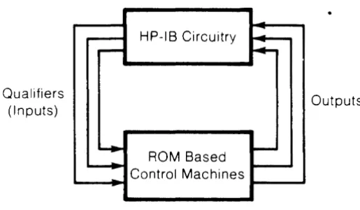
The PHI access control and byte packing control machines are ROM-based, state oriented logic circuits which receive input signals called qualifiers from the other HP-IB board circuits and generate control signals called outputs. This structure is depicted in Figure 3-1.
Qualifiers (Inputs)
~ ~
:...
-...
HP-I B Circuitry
ROM Based Control Machines
~
~
Outputs
-Figure 3-1: Basic Control Machine Structure
The inputs, or qualifiers, give the control machines information about the present state of the hardware.
The control machines decide what action should be taken and then what outputs should be given to stimulate the hardware to perform the necessary task.
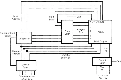
The controllers are designed to make decisions by programming the bit patterns stored in ROMs. Two bits of the present state and three alternate/ direct bits determine the five bit ROM address. The alternate/ direct bits are also stored in ROM but are selected based on the status of the input qualifiers. Thus, the ROM address is determined by the present state and the input qualifiers. The state of the ROM is updated on the leading edge of a six megahertz clock signal called CKl. That is, new states or new addresses become valid and a ROM memory location is accessed on CKl.
The ROM output words contain four parts: 1). Four bits are used to select the appropriate input qualifier to be used in determining three bits of the next state. Three of these four select bits are also used as the alternate address bits; 2). Seven (PHI acess) or ten (byte packer) bits are used as outputs; 3). Three bits are used as the direct address.; 4), Two bits are used as next state bits. These outputs become valid on the leading edge of a six megahertz clock signal called CK2. The CK2 signal is essentially an inverted CKI signal.
[image:36.615.197.455.215.365.2]30
Theory of OperationAlternate D Selec t
Direct Address
Irect
-
MultiplexerAlternate Address
~ Oualifier
Select
I I I I I
Controller Inputs (Qualifiers)
Next CK1
State
I
-
--Addr~ss
State Bits
Latch
[image:37.617.33.541.96.430.2]Ouallfier Select Bits
Figure 3-2: Structure of the Controller Circuitry
I
ROM Outputs
I n
P u t s
J
ROMs
ROM Outputs
7 To 10
Output Latch
7 To 10
Controller Outputs
r--CK2
Decisions are executed in the state machines by selecting either the alternate or the direct address as the next state. Whether the direct or alternate address is selected is determined by the state of the AL TERNATE/ DI-RECT SELECT pin on the multiplexer. A logic one level selects the direct address and logic zero level selects the alternate address bits. This line is driven by the input qualifier which is selected by the four Qualifier Select Bits. Notice that three of these bits also serve as the alternate address bits. Thus, in the present state, a particular qualifier is selected and its logical value controls whether the next state is the one pOinted to by the direct address or the alternate address. In this manner branching is implemented in the controller algorithm.
Theory of Operation
31
o
Load 1st Byte In FIFO
26
r - -... ---, Last Word Has Been Loaded
Is PHI Access Control Done?
Request Interrupt
Wait for Interrupt Service
"Ctean Up"
NOTE
All states are 10 octal notation.
The logic stales shown in this diagram are defined as follows:
1 = high = ;.2V 0= low = ~.8V
Byte-Packer
Qualifier Assignrrlents
NO-OP MT DMARIP DMR DMW SDR QIOSB STWR STRD 10SBF DR LW IRCL
Load 1st Byte In 110 Latch. Set DMA Request
Still In Burst Mode?
05
---''--~
DMAC Equal Zero?
Has Last Byte Been Transferred?
r----1._--i06
14
07 04 11 00 17 02 01 10 12.03 05 06.13 16
Theory of Operation 33
r - - - ,
I
I I
I
I
I
Programed 1/0
Get Data From PHI
Dala Ready?
Is 1/0 Bus Cycle Done?
_--,r-... Access Instruction
L _ _ _ _ _ _ _ _ _ _ _ _ _ _ _ _ _ _ _ _ _ _ _ .J
1
NOTE
All stales are in octal notation.
The logic states shown in this diagram are de-fined as follows:
1 = high = ~2V
0= low = ,,;:.BV
PHI Access Control
Qualifier Assignments
NO-OP 03
DMR 00
ORE 05
IOEND 07.17
LBT 04
DMW 13
BFULL 15
STPW 11
PAC 02
WRITE 12
STBF 06.16
QUIT 14
PH! RegIster Access?
15 FIFO Room AV3013ble? DMA Read?
r--= ... =---, Tell By1e-Packer
07
r - - - ' - - - " DMARIP
lOGO TOPF
Send Data To PHI
Get New Data Upon LeaVIng State
Wait For PHI To Accept Data
Decrement ShIft RegIster
Has Last Byte Been Transferred?
Wait For New InstructIon
Service 35
Servicing the Disc Interface
Disc Interface Disassembly Procedures
The following proceedures outline steps that can be used to remove each of the assemblies in the disc interface for service.
WARNING
DISCONNECT THE AC POWER CORD BEFORE ATTEMPTING TO DIS-ASSEMBLE THE DISC INTERFACE.
Disconnect the disc interface from both the computer and the disc controllers in the system.
Tools Required for Disassembly
The following tools are needed to disassemble the disc interface:
• Large pozi screwdriver
• Small pozi srewdriver
• Small flat blade screwdriver
• Diagonal wire cutter
• 7mm open or box end wrench
36 Service
Al and A2 Assembly Access
The Al and A2 assemblies are contained in the interface card case. Follow these steps to remove the A 1 and A2 circuit boards from the case.
1. Remove only the four screws shown in photo A of Figure 3-3. Then flip the interface over and remove the four screws as shown in photo B of 3-3.
2. Pull the rear housing from the front housing and separate the two halves of the front housing case as shown in photo C of Figure 3-3. The Al and A2 boards are held together by three connectors. Carefully separate the circuit boards by pulling them apart.
A. B.
'~, ,
[image:41.613.31.538.255.692.2]....
Service 37
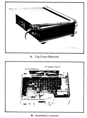
A3 thru A7 Assembly Access
The A3 thru A 7 assemblies are located in the central data unit. The following steps can be used to access these assemblies.
1. Unfasten the screw located at the rear of the top cover (photo A of Figure 3-4) with a large pozi-drive screwdriver. This screw does not come out of the cover.
2. Slide the cover to the rear of the unit and remove it as shown in photo A of Figure 3-4.
The location of the various assemblies is shown in photo B of Figure 3-4.
A. Top Cover Removal
A3 Su rt Board A4 HP-IB Board
/
[image:42.613.185.465.257.638.2]B. Assembly Locations
Figure 3-4: A3 thru A 7 Assembly Access
NOTE
Service
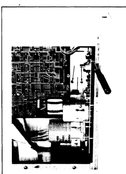
39
A. Removing the A6Wl cable and the location of the three heat sink mounting screws.
[image:43.617.217.437.93.394.2]B. Removing the right side panel and the location of the five board mounting screws.
Service
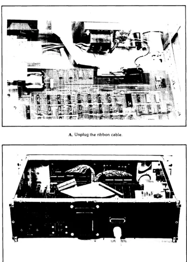
41
A. Unplug the ribbon cable.
[image:44.615.142.510.90.604.2]B. Remove these metric screws.
Service 43
~
'~""i -~'
At·
B. Remove these 'r4 inch nuts.
[image:45.618.135.523.88.654.2]C. Carefully pull the cable through the hole.
Figure 3-9: Removing the A 7 I/O Cable Assembly
Service 45
Adjusting the
PHI
Internal Timing
Whenever the PHI chip is changed. the internal timing delays must be adjusted. Potentiometer R2 on the A4 HP-IB board is used to adjust this timing delay. An oscilloscope (or some other type of test equipment that is capable of measuring a pulse width independent of frequency) is required for the adjustment.
Procedure
WARNING
This procedure requires that power be applied to the disc interface. Lethal voltages exist throught the primary circuits of the power supply. DO NOT TOUCH any of the primary circuitry.
Connect the 98041A I/O card to a System 45 computer. All cables from the mass storage controllers should be disconnected from the 98041.
Connect the oscilloscope probe to the test point marked "HSE/ PUE", located near the PHI chip on the A4 board (see Figure 3-12). Connect the probe ground lead to the nearby test point marked "GROUND" .
•
[image:46.615.122.540.421.694.2]'~~."""'''''''''''''7''-'···'~'';'I'''fII!/!II''''~~ _~"fii"'I'IIIiI~'I/.'~!/jI/'/_~?/I1"IIff!~"'fi""i,.~/!!f!!II'!!IIIfIfflfiH""'I'!~~~I'fIId:I!fFI''H'1''.'''''«:"'·'
Service 47
Availiable Field Service Inventory Items
Assembly
Reference HP Part No. Qty Description
Al 98041-66501 1 I/O Control Board
A2 98041-66502 1 1-6)0 Data Logic Board
A3 98041-66504 1 Support Board
A4 98041-66507 1 HP-IB Board
A5 98041-66505 1 HP-IB Connector Board
A6 98041-66503 1 Power Supply Board
A7 98041-61602 1 I/O Cable Assembly
A4U1 1AA6-61606 1 PHI Chip
A5W1 98041-61606 1 D. C. Power Cable
98041-61603 1 Power Switch Assembly
10631B 1 2 Metre HP-IB Cable
[image:47.612.129.508.128.353.2] [image:47.612.177.472.402.696.2]98431A 1 Mass Storage ROM
Figure 3-13 shows the Product Support Package and the location of each of the components.
Installation and Service Manual
Alii 0 Control Board A2 I/O Data Logic Board
A6 Power Supply Board
Parts Container
(linear I.e.. XSTR, F~~
Signal Line Name Abbreviations
Abbreviation IRCL IRL ISB LBR(N) LBT LOAD LTEI LTEll LW(N) LWIN MT OFB ORE OSB PAC PAO-PA3 PL POP QIOSB QUIT RPRO RST SDR SETDR STBF STPW STRD STS STWR WRITE(N) WIR5 TOP TOPF TOPS MeaningInterrupt is Cleared Low level Interrupt Line Input Second Byte Last Byte Ready Last Byte Transferred Load 1/0 Latches Less Than or Equal to 1 Less Than or Equal to 11 Last Word
Last Word In FIFOs Empty Output First Byte Output Register Empty Output Second Byte PHI Access
Peripheral Address Select Lines Parallel Load (into FIFOs) Power On Pulse
10SB qualified with PA 10END "ORed" with LW Read PHI Register Zero Reset
Sampled Data Request Set DMA Request Strobe Finished STOP Write START Read Status (lOC signal) START Write
Write PHI Chip Registers
Write Instruction Register due to W5 Transfer Out Parallel
Transfer Out Parallel (FIFO)
Transfer Out Parallel (Shift Register)
REFERENCE DESIGNATOR Al C1 C2 C3-C7 RI-R4 SI U11 U2 U3 U4 U5 U6 U7 U8 U9 UlO U11 U11 XA2Pl.XA2P2 XA2P3
Al Replaceable Parts
-"p-
TQ DESCRIPTION PART NO.98041-66501 I/O Control Assembly 0160-3847 6 C-F .01ILf 50V 0180-0106 1 C-F 60ILf 6V 0160-3847 C-F .01ILf 50V 0683-2225 4 R-F220005% 3100-3364 1 Select Code Switch
820-1427 1 IC SN74LS156 1820-1282 1 IC SN74LSI09 1820-1211 1 IC SN74LS86N 1820-1204 1 IC SN74LS20N 1820-1199 2 IC 74LS04N 1820-1491 1 IC SN74LS367N 1820-1245 1 IC 74LS155 1820-1208 1 ICSN74LS32 1820-1199 IC 74LS04N 1820-0327 1 ICSN7401N 1820-1414 1 IC 74LS12N 1820-1199 IC 74LS04N
2 Connector 15 socket 1 Connector 9 socket
Al Component Locator
'8
14,
U9
rl.:L
o U
Service
51
~I~ ~ONT-ROL-BOA~O- (-98-04-'-66-5~J - - -
-:
I
I
~I~
~R3 jR4 ~RI ~R2 L200 ~ 2200 ~ 2200
J 2200
+5V
I
CONNECTS SHIELD ---< 17~' + + + F "
-~C:B~~'~L PAO ---< 13f-(
---+-1
-+-j+-1
+--~~----_ -_:-3:::=:
=========::f
1=11
==
I I I
I I !
. . +12V ~
III
--<. 18 ~ NC I v I
I I I
r+
---< v (-12V N C ' II II' II' ~2' USA' I I
I
I II~'
1 I I
II',
11
4:
~L:
+5V ---<
AI
\zlc,l
c31 c4lcJ c6lc71
II
II! '
'''--<I
(oorrrrrr-;Ti
IIII
jlj
;~§'i~l
_ 1
+---+-.
-+-+--+--111~
l_+___
I
/RL ---< 12
I
I I I
~
I
I
I
I . - - - . 9 s JUII :~ ' j
I
~
I
1
6 ,I 12 I
UII
"- 5
i
, I
FLG ---< .. r' utOD l'2 '
1
I
~9'
IO<UlOC I.
~ SfS ---< N
6 j
0iiAR--< u .~
i--+5V !
I
I008~6
IOD 9 F
laD 10 7 100 II H 10012 e 100 13 J
lao 14 9
i5O"i5 K
I
!
I
I2 STATUS I I I
UIOA '!.~9 I
-«::::J
\~i~l~l---1007---< E
~i
---L _______________________ .
9804/-51281
'1' ,
-C\lrt)~
:::0:0:0:
I ~ ~
.I
lU9r~
''11-66501
Service 51
fAlTl~ ~~~D- (~~I-- - - - - - - - - - - ,
~ f I I
I I
11.1.\.212]'
01¢
t~~oo ~~ ~~~~~oo
I
SWITCHI
IIii'!I
"'1'-" ,-"'''
+5V XA2P~ I ~~1~~\ t&9tT~OARO
1 ""SB 17 16 ". ~SB I I I
CONNECTS SHIELD ----< 1 7 < ; : - - - + - i _ r - F = - - - -______________________ -+-<1 ( 39 f+--SHIELD
~=~~~~:---tl,l-lHj'11---~~~,1~~~:~:_~_·~2i·~P6~5~~~~-~~
-
~~~.-m --< 16
~
t-~f-+. -+.---~~~~~~~~~---'--'!:"'--I~..)~, r~::~;"'--:'--___"l:"
I
vI
{f~
j:
tL
I
I I I I
r~---
__
----4_--~~---~:(7~MY~
+i2V ! I I ! ! ~r--l
I
~:~:
~Ii"~r
II
iii
I
~I'
II~ mt~,II~~~~~~~~~~~~~~~~~~~~~1(91
I
I I~
I U7tyO I+5V--<A
I
~\2-1cl-.-lc-31---<c41~c5-.-lc-61---,C71!
[ I I !III
~,:
-
~~II!':;
2Y 'Ylln II'_---jil _ _ _
~il _I~
=R5OUT~_rIR"""t5SB412cK:~;al"'c---K"~ ~'NTEN
GN°---<I'
(60rrOlOTOlrOT~;r!i!
I,II'
II
~I
ill~
I~II
II' r---+-i:
_~_:~_88_6
+-+T-"-I14 J U2B .-- I~
r---+---f--+--"~K _ Q ~ I~J!N
!
1
1 5 ! ~~- T ..10SB--<S<;:---T,----+---+~-i-~-i---+---+~--~~1'~6A G'6Y~I'~~~-_+---i_~--+_--+_---_r<
°Wr
~l~ :~ :: :~ .~I5===<P 6 ~u63r~7-~~-_+---i_~--+_--+_---~
~
--<I
1 ;
~~~=t::t===tl ========t=:t===t===::t=================================~
I
I II
9 8I
10 USC
9
-.
~ 13 I~
!6 3 "
~ i
IJ
UIOO 1,2
I I +:>V
1
L
I • CK a •
I
i
3 j(
I
U2A
~J li~N.C.
---r
~ ~IIE---_+----~
ill --< 12 E---_+--~
FLG --< .. ~ (---_+----'''<1
9 i
10 '"\ UIOC IB
~
I
6
.~ f---+5V !
j
1
O~R---<UE---+----~
I
I~;,~~~~--~---+---+---~~r-i---+---+_+_+__+---+---~---T{
IDDII
H~--i_---~---~---i_r_~---+---+_6-1_~---+_---T~moTI Bf---+_---;---+---~~-~---~---+---+__+---+---T<
10013 J f---+_---+---+---~~r-~---~---~---+---+__+---+---r<
IDOl4
9<;:---+---T---+---~~--i_---r---+_--+__+---+---r<IDOl5
KE---+---+---+---~~--i_---_+---+_--+__+---+---T{I
1
---r---~----_ri===================================r==1~I~
~==~
~~======~i5~'~~~'~9~====~---f,l!~I1.---lr--~
I ~ESP 10
I UIOA 2, sr:U~9 i L----~---~--~i--~:~2 U4BJ»2-S-+-11 ... ---""'-!. E~~
II
U913
'::J L - - - t ; - 2 ---'~+_--~2'-lJ UI I,V::~
I
.&9~
~~
II
I IE!~~
~~E!
100 3 C 22 100 3
roo 4 4 21 lo]j4
iOD5 0 20 ' TOo5
1006 5 - - _ . 19 iOD6
1007 E 18 ~T0D7
L ___ - - - ___________
--- ---~98041-51281 (ORIGINAL)
Service
53
A2 Replaceable Parts
REFERENCE -hp- TQ
DESCRIPTION DESIGNATOR PART NO.
A2 98041-66502 1 I/O Data Assembly
C1,C2 0160-3847 6 C-F .00~f SOV C3 0180-0160 1 C-F 60~f6V
C4-C7 0160-3847 C-F .00~f SOV P1,P2 2 Connector IS PIN
P3 1 Connector 9 P / N RI-R6 0683-471S 10 R-F 470n S% R7-R14 0683-7S1S 3 R-F 7S0n S%
I
RlS-RI8 0683-471S R-F470n S% R19-R42 0683-7515 24 R-F7S0n S%
U1 1820-1416 1 IC 74LS14 U2-U7 1820-1491 6 IC SN74LS367N
A2 Component Locator
:
(.---'~4--i:
~
u~; ---~
__ JIlT-'fJ
I
I
~. ~;~-
-:,,-. .--:".:±--,: --,,---" -" --
-:::"t,
:,,1
---&...I-_~ ~ ~ : ~ N 2 po. !:: !Q c _ _ _ _ _ _ _ _ ~ ~ j;) I)f ~