http://www.scirp.org/journal/opj ISSN Online: 2160-889X ISSN Print: 2160-8881
Identification and Analysis of Hazardous
Materials Using Optical Spectroscopy
Surik Khudaverdyan
1, Vazgen Meliqyan
1, Taron Hovhannisyan
1,
David Khudaverdyan
1, Ashok Vaseashta
2,31National Polytechnic University of Armenia, Yerevan, Armenia 2International Clean Water Institute, Manassas, VA, USA
3Institute of Electronic Engineering and Nanotechnologies “D. GHITU”, Academy of Sciences of Moldova, Chisinau, Moldova
Abstract
This investigation is aimed towards using optical spectroscopy for remote identification and quantitative analysis of hazardous substances for safety and security applications. We introduce a new model employing portable photo-sensor devices that are based on the double-barrier and vertically placed sili-con structure, for such applications. The different absorption depths of indi-vidual waves allow us to carry out their spectral selection using an algorithm developed for this specific objective. We tested the proposed model on expe-rimental Ag-p-Si-n-Si structures. The algorithm is developed for the spectral analysis without the preliminary calibration. The low dark currents (several dozens of pA) permit us to carry out the spectral analysis of the integral flux of the electromagnetic radiation of low intensity. The quantitative data from light current-voltage characteristics allow us to obtain an intensity distribu-tion spectrum characteristic of the material by using red LED and the green laser. The results of this investigation divulge new possibilities for the creation of a new type of the portable semiconductor spectrophotometer and due to its stand-off detection capability, offer potential pathways to evaluate hazardous substances.
Keywords
Distribution Spectrum, Photosensors, Optical Spectroscopy, Radiation Intensity
1. Introduction
In recent years, increasing demand for the stand-off detection/sensing for ha-zardous chemical has significantly increased due to their use in safety, security, environmental protection and detect suspicious packages, wire, fragmentation How to cite this paper: Khudaverdyan, S.,
Meliqyan, V., Hovhannisyan, T., Khuda-verdyan, D. and Vaseashta, A. (2017) Iden-tification and Analysis of Hazardous Mate-rials Using Optical Spectroscopy. Optics and Photonics Journal, 7, 6-17.
http://dx.doi.org/10.4236/opj.2017.71002
Received: December 14, 2016 Accepted: January 19, 2017 Published: January 22, 2017
Copyright © 2017 by authors and Scientific Research Publishing Inc. This work is licensed under the Creative Commons Attribution International License (CC BY 4.0).
http://creativecommons.org/licenses/by/4.0/
materials, or other signs of improvised explosive devices (IEDs) or crisis situa-tions. Standoff techniques enable detection of threats without contact. The pos-sibility of contamination (for operators and/or equipment) is thus avoided, and the need for subsequent decontamination is eliminated. In addition, standoff detection of explosives allows identification of threats from safe distances, i.e., outside the blast zone. There are now ongoing efforts to extend these methodol-ogies to even biological threats. It is, hence of paramount importance to increase the efficiency of such methods and solution pathways which will respond quickly to such crisis situations. It is particularly important to create user-friendly sen-sors platform which will likely enable the remote analysis of the different mate-rials in different media.
Remote spectrophotometric sensors are of special interest these days, as they provide us with necessary information on the composition of the mediupm un-der investigation and hence solve the omnipresent problem of identification from the security stand-point [1] [2] [3] [4] [5]. Nevertheless, the information received from studies of natural objects by existing means is not satisfactory from the point of their quantitative and qualitative analysis. There is a signifi-cant gap in terms of dispersion of the spectral data of the identical objects even in the advanced methods of investigation of the optical spectral analysis, which often excludes correlation between the measurement results. The processing of the spectral data is obtained by quantitative analysis and the reliability of such results depends directly on the parameters of the device in use.
It is critical that several sensors are required for monitoring large areas. To optimize cost and to strategically place sensors in regions which are likely to provide a fair assessment of the contamination scenario, it is urgent to develop; a): inexpensive and small-size sensors with high spectral sensitivity, suitable for remote field identification, and, b): appropriate algorithms for accurate registra-tion of data measured by these sensors. In methods that are currently available for spectral analysis, the spectral distribution of the electromagnetic radiation is obtained by light filters, a prism, a diffraction grating and high accuracy me-chanical devices [6] [7] [8]. The spectrophotometric systems like this are not multi-purpose and require additional devices and external software support for the fulfillment of every new function. Thus, they are rather expensive and are not suitable for field deployment.
ab-sorption conditions with nanometric accuracy for multiple photodiodes and multilayer structures. The complexity involved during fabrication of photodi-odes and multilayer structures during their development and the difficulty in controlling the spectral sensitivity by the external voltage impedes their devel-opment and usage. The present investigation offers a viable means of high level of accuracy during spectral analysis with the help of the electronic processes in n+-p-n+ structures.
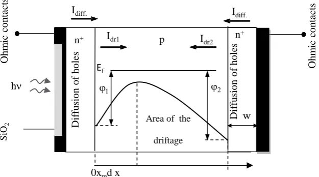
2. Device Structure
The structure under investigation is a silicon structure, as prepared using stan-dard integrated circuit processing methods. The structure consists of an n+-p-n+ structure (Figure 1). The p-base is occupied by the depleted layers of two bar-riers (Figure 1). The current through the structure is the difference of the cur-rents of the two oppositely directed potential barriers. The position of the point of contact of the depleted layers xm (Figure 1) depends on the polarity of the ex-ternal voltage and is moved to the surface of the forward biased n+-p junction (ohmic contact). The electromagnetic radiation is incident on the left ohmic contact as shown in Figure 1. The registration area of the radiation is in the depleted layers. In presence of applied voltage, the reverse biased n+-p junction is dominating and thus it’s depleted layer becomes wider. In the meantime, the depleted layer of the forward biased junction becomes thinner. As a result, the current is mainly governed by the reverse biased p-n+ junction. The incident electromagnetic waves have different penetration depths with respect to their wavelengths and intensities.
[image:3.595.218.531.541.715.2]Since the shift of xm towards the surface (towards “0” in the Figure 1) widens the range of current generation, different waves contribute according to their wavelength. The thin p+ layer towards the left surface with high conductivity can be neglected, the “0” point can be taken as the surface, and the voltage drop at the front contact can be neglected. This allows us to measure of the photocurrent which contains information with respect to their wavelengths and intensities.
Figure 1. n+-p-n+ structure and the directions of currents in it. ϕ1
w
O
h
m
ic co
n
tact
s
D
iffu
si
o
n
o
f
ho
le
s
D
iffu
si
o
n
o
f
ho
le
s
n+
EF
p
hν ϕ2
Area of the
driftage
Idr1
O
h
m
ic co
n
tact
s
Idiff.
Idr2
Idiff.
S
iO
2
0xmd x
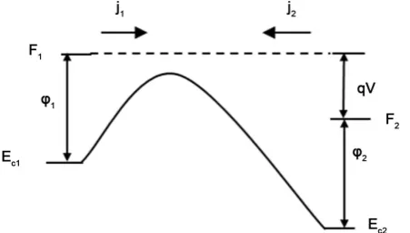
The information can be obtained by a relevant algorithm. For the develop-ment of such algorithm, it is necessary to find the relationship between xm, ap-plied voltage V, absorption coefficient α and incident intensity F. Considering that the base is covered by the depleted regions of both barriers, we determine the distribution of potential in the spatial charge region of the double-barrier structure, as shown in Figure 2. For this, we solve the Poisson equation which connects the field potential V x
( )
with the volume density of the chargescreating the field,
( )
2
2
0 d V x
dx
ρ εε
= − (1)
In Poisson’s equation, the potential V x
( )
can be related to the potentialenergy of electrons ϕ
( )
x , as, (ϕ( )
x = −qV x( )
).Since ρ =qNa, we obtain,
2 2
2 0 a N q d
dx
ϕ εε
= (2)
where Na is the concentration of acceptor impurities, ε is the relative dielec-tric permeability of the substance, ε0 is the dielectric permeability of the
va-cuum, and q is the electron charge.
The boundary conditions for the given equation are d 0
dx
ϕ
=
at x=xm (Figure 2, xm is the minimum of the potential energy of electrons) and
( )
x 1ϕ =ϕ at x=0 (Figure 1).
Taking into account the boundary conditions, we integrate Equation (2) and obtain,
( )
2 2 21
0 0
2
а а
m
q N q N
x x x x
ϕ ϕ
εε εε
= − + (3)
When x=d (Figure 2).
( )
2 2 21 2
0 0
2
а а
m
q N q N
x d x d qV
ϕ ϕ ϕ
εε εε
= − + = +
It is possible to find the dependences of xm and d−xm on the external vol-tage:
[image:4.595.263.489.585.713.2](
)
0 2 2 m а V d d xq N d
εε ∆ +ϕ
− = + (4)
where ∆ =ϕ ϕ2−ϕ1.
If both barriers are identical, then ϕ ϕ2− 1=0. Consequently:
0 2 2 m а V d d x
q N d
εε − = + 0 2 2 m а V d x
q N d
εε
= − (5)
With the help of Equation (5), we can determine the modulation depths of depleted layers, and the position of xm. Using, ∆xm =xm2−xm1, we can
deter-mine the wavelength and the intensity of the absorbing radiation.
For that, we first determine the total photocurrent flowing through the struc-ture. In the investigated photodetectors, the photocurrent has diffusion and drift components. To determine the diffusion photocurrent, it is necessary to find pn density of minority charge carriers-holes in the n-semiconductor. For that, the following one dimensional diffusion equation is solved [18],
( )
2
0
2 2 2
n n n
p
p p
G x
p p p
D
x L L
∂
− = − −
∂ (6)
where Lp= Dpτp is the diffusion length of acceptors in the n+-region,
( )
0x
G x =F
α
e−α is the generation rate of electron-hole pairs, F0 represents thetotal flux of incident photons, α represents the absorption coefficient of
elec-tromagnetic radiation, Dp is the diffusion coefficient of acceptors in the n+-re- gion, τp the lifetime of excess charge carrier-acceptors and pn0 represents the
equilibrium density of acceptors in the n-region. The solution of Equation (6) under the boundary conditions pn = pn0 at х = ∞ and pn = 0 at х = d (pn—is the concentration of minority charge carriers in the rear n+-region) is
0 0
1
p p d
diff n
p p
D L
I S qp qF e
L L α α α − = + +
(7)
Khudaverdyan et al. [19] obtained an expression for the drift currents gener-ated in the base of such structures:
(
)
1 0 1
m x dr
I =qF S −e−α (8)
(
)
2 0
m
x d
dr
I =qF S e−α −e−α (9)
where α is the absorption coefficient of the electromagnetic radiation, S—the
photosensitive area and F0 =Popt
(
1−R)
S hν—the total flux of incidentpho-tons per unit area. Popt—the radiation power, R—the reflection coefficient, h— Planck constant, ν—the frequency of the electromagnetic radiation and q—the
electron charge.
1 2 0 1 2 0 1 m d p x
tot dr dr diff p
p p
D e
I I I I S qF e qn
L L α α α − − = − − = − + − +
(10)
At normal functioning, the term that contains np0 is much smaller than the first term. Thus, it may be neglected, and Equation (10) is:
0 1 2
1 m d x tot p e
I q S F e
L α α α − − = − + +
(11)
When irradiated by the integral flux (e.g. of the Sun), Equation (11) for the photocurrent is:
( )
, 1 , 2 , ,
, , , , , 1 2 1 i i mj
Ph i j dr i j dr i j dif i j
i j i j i j i j
d x
i
i j i
I I I I
e
S q F e
w α α λ α − = − − = − + +
∑
∑
∑
∑
∑
(12)where (i = 1, 2, 3, …) changes in the integral flux with the change of the emis-sion wavelength, and (j = 1, 2, 3, …) changes with the change of bias voltage,
F0(λi) is the total flux of incident photons with the wavelengthλi.
Since the width of the n–region in Equation (11) was less than Lp, the value of
Lpin Equation (12) was replaced by W (Figure 1). Using algorithm described below, it is possible to register a separate wavelength λi and its intensity by changing the voltage ∆V, thus obtaining the spectral dependence for wave intensities.
Let us consider some peculiarities of detection of separate waves in the integral flux of radiation using structure containing oppositely directed potential barriers. Such scenarios are used for detection of certain wavelength and its in-tensity under the conditions of the wave absorption and emission (fluorescence) of the objects under investigation.
In the present investigation, we used the AM0 spectral distribution for Si us-ing radiation of LED (L-813SRC-J4) with a dominant wavelength 660 nm and a laser with the radiation wavelength of 530 nm. Since, with increase of the bias voltage, the registration region of the rear barrier widens towards the surface [19] [20], it allows us to carry out the sequential registration of the waves from depth to the surface.
3. Result of the Experiment
To determine the spectral composition of an integral flux of the electromagnetic radiation, the wave intensities of the radiation are equally divided so that the absorption depth corresponds to the width of the registering environment (~4 - 6 μm). The photocurrent corresponding to the largest possible value of x is nor-malized by the most deeply penetrated wave. Under these conditions, the process of the selection of separate waves and their intensities from the integral flux of radiation can be described as in the following.
vol-tage 1 mV, and the relevant photocurrents I1 and I2. They are obtained only from the absorption of the most deeply penetrated wave λi. With the help of these photocurrents, and using Lambert’s law on radiation absorption in the homoge-neous environment, we will have the coefficient of wave absorption,
2
1
1 ln ,
i
I
x I
α =
∆ (13)
where ∆ =x xm2−xm1.
Using α= f
( )
λi and Equation (13) with the corresponding program, wecan determine the length of the wave for the initial material of the photodetector, e.g. silicon. By means of the formula for the photocurrent (11), we can obtain the intensities of separate waves in the absorbed radiation as,
0
1 2
1 i i m j
i
i d
x
i I
F
e
q S e
w
α α
α
− −
=
− +
+
(14)
With the help of Equations (5), (13) and (14), we determine the absorption coefficient of the most deeply penetrated wave, the wavelength and the intensity of the wave. Then, with the help of the expression (12), considering the absorp-tion surface, we form the dependence I1 = f(V) and subtract it from the experi-mental dependence I = f(V) of the summed current. As a result, we obtain a new dependence of the summed photocurrent on V, without the dependence I1 =
f(V).
By means of relevant software, this method helps us determine the lengths and the intensities of all the waves in the radiation. The experiments were carried out on the n+-p-n+ structure. The cross-section of the structure with the parameters of the layers is presented in Figure 3. The spectral region of the monochromator is from 400 nm up to 1150 nm. Based on these parameters, the design height of the rear barrier was φк = 0.89 eV, and the distance of Fermi level from the va-lence band top of the p-epitaxial layer was EF − EV = 0.29 eV (Figure 4). The height of the silicide Schottky barrier (p-silicon with Ag) was 0.54 eV [18], and, consequently, the height of the surface barrier was ϕc = 0.25 eV.
The photocurrents of the two oppositely directed barriers are oppositely di-rected, and they compensate each other depending on the applied voltage. It is noticeable in the relative spectral characteristics (Figure 5). The figure shows the mirror image of the long wave photocurrent. In the absence of the bias voltage (Figure 5, curve. 1), the spectral photocurrent is mainly governed by the surface potential barrier, which creates a short-wave peak.
Figure 3. Cross-section of the structure and the parameters of individual layers.
Figure 4. Energy band diagram of the structure.
Figure 5. Spectral distribution of the photovoltage on the load resistor of 0.5 MΩ. EC
EV φc= 0.89 eV
EF-EV= 0.29 eV
φc= 0.25 eV φSch= 0.54 eV
[image:8.595.257.495.546.715.2](Figure 5, Curve 3), and the long-wave peak becomes more noticeable. Such mutual compensation of the photocurrents of both barriers is related to the change in the width of the wave registration region.
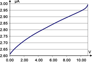
Thus, at different voltages, different waves penetrate into the registration re-gion of the rear barrier. These waves determined by the corresponding change of the photocurrent. During the experiment, for determining the spectral distribu-tion of the intensity of the absorbed radiadistribu-tion, the L-813SRC-J4 LEDs and laser beam (wavelength of 530 nm) were used. The experimental current-voltage cha-racteristic in the dark (Figure 6) showed that in the wide range of the bias vol-tage, the currents had small values (several dozens of pA). The photocurrents had the values of several μA (Figure 7). Several orders of the difference of light and dark currents allowed us to register low fluxes of light signals with the help of the test samples.
[image:9.595.274.474.402.548.2]The design width of the depleted layer of the n-p junction under the zero bias is ~1 µm, and 2.55 µm under the reverse voltage of ~5 V. Thus, we observe the modulation of the width of the registration region of the rear barrier. With the help of Equation (13) and (14), the current-voltage characteristic data in the dark and under illumination, and the developed algorithm [21], we modelled the process of receiving of the spectral distribution of the radiation intensity. As a result, the received spectral curve (Figure 8) is close to the stated curve of the red LED and the laser with the radiation wavelength of 530 nm (Figure 9).
Figure 6. Voltage-current characteristic of the sample in the dark.
[image:9.595.275.472.583.717.2]Figure 8. Spectral distribution of radiation intensity.
Figure 9. The spectral distribution of the laser wave.
4. Conclusions
We have developed a new model of the portable photosensor for the remote identification of optical information. Different absorption depths of electro-magnetic waves in the developed silicon photodetector are used to create an algorithm for the determination of the wavelength and its intensity.
Experimental samples have been investigated and possibility of selective spec-tral sensitivity in them has been proven. That is possible thanks to variation of potential barriers in bases of the samples at the expense of each other when applying external voltage.
Spectral distributions of intensities of red LED and the laser with the radiation wavelength of 530 nm have been received using the developed algorithm. It repeats the reference distribution, with certain approximation.
[image:10.595.212.538.255.499.2]new possibilities for the creation of a new type of the portable semiconductor spectrophotometer. The developed algorithm is used to carry out the spectral analysis without a preliminary calibration.
Acknowledgements
The authors express their gratitude to the company “RD ALFA Microelectron-ics” for their assistance in the prototyping of the sample photodetectors. We also acknowledge support of NATO Science for Peace and Security-G4403 for partial support of this investigation.
References
[1] Jiang, P., Xia, H.B., He, Z.Y. and Wang, Z.M. (2009) Design of a Water Environ-ment Monitoring System Based on Wireless Sensor Networks. Sensors, 9, 6411- 6434.https://doi.org/10.3390/s90806411
[2] Normatov, P.I., Armstrong, R., Normatov, I.Sh. and Narzulloev, N. (2015) Moni-toring Extreme Water Factors and Studying the Anthropogenic Load of Industrial Objects on Water Quality in the Zeravshan River Basin. Russian Meteorology and Hydrology, 40, 347-354.https://doi.org/10.3103/S106837391505009X
[3] http://augsignals.com/products-services/water-quality-monitoring/
[4] Vaseashta, A. (2015) Life Cycle Analysis of Nanoparticles-Risk, Assessment, and Sustainability. Destech Publishers, New York, 404 p.
[5] Vaseashta, A., Braman, E., Susmann, P., Dekhtyar, Yu. and Perovicha, K. (2012) Sensors for Water Safety and Security. Surface Engineering and Applied Electro-chemistry, 48, 478-486.
[6] Pshinko, G.N., Kobets, S.A. and Puzyrnayain, L.N. (2013) Concentration of U(VI) on a Complexing Sorbent for Its Determination by the Spectrophotometric Method. Journal of Water Chemistry and Technology, 35, 145-151.
https://doi.org/10.3103/S1063455X13040012
[7] http://www.shimadzu.com/an/uv/support/fundamentals/structure.html
[8] http://www.dissercat.com/content/razrabotka-i-primenenie-distantsionnykh-spektr ometricheskikh-metodov-issledovaniya-prirodnyk
[9] Kautzsch, Th. (2013) Photo Cell Devices and Methods for Spectrometric Applica-tions. Patent US 20130285187 A1.
[10] Kautzsch, Th. (2014) Photodetector with Controllable Spectral Response. Patent US 8916873 B2.
[11] Kautzsch, T. (2012) Photocell Devices and Methods for Spectroscopic Applications. Patent DE 102013207801 A1.
[12] Jan, C., Daniel, P., Man, S.T. and Univ, N. (2005) Photodetector with Controllab-lespectral Response. Patent US 8916873 B2.
[13] Nataša, G. and Novel, A. (2007) Type of Tri-Colour Light-Emitting-Diode-Based Spectrometric Detector for Low-Budget Flow-Injection Analysis. Sensors, 7, 166- 184. https://doi.org/10.3390/s7020166
[14] Elif, Ç.S., David, S.F., Mutlu, G., Ekmel, Z., Mesut, S. and Selim, M. (2014) Im-proved Selectivity from a Wavelength Addressable Device for Wireless Stimulation of Neural Tissue. Frontiers in Neuroengineering, 7, 5.
00072.
[16] Vanyushin, I.V., Gergel, V.A., Zimoglyad, V.A. and Tishin, Y.I. (2005) Adjusting the Spectral Response of Silicon Photodiodes by Additional Dopant Implantation. Russian Microelectronics, 34, 155-159. https://doi.org/10.1007/s11180-005-0024-5 [17] Gergel, V.A., Lependin, A.V., Tishin, Y.I., et al. (2006) Boron Distribution Profiling
in Asymmetrical NC-P Silicon Photodiodes and New Creation Concept of Selec-tively Sensitive Photoelements for Megapixel Color Photoreceivers.
[18] Sze, S. (1981) Physics of Semiconductor Divices. 2nd Edition, Wiley, New York, 450.
[19] Khudaverdyan, S., Petrosyan, O., Dokholyan, J., Khudaverdyan, D. and Tsaturyan, S. (2012) Modeling of a New Type of an Optoelectronic Biosensor for the Moni- toring of the Environment and the Food Products. In: Vaseashta, A., Braman, E. and Susmann, P., Eds., Technological Innovations in Sensing and Detection of Che- mical, Biological, Radiological, Nuclear Threats and Ecological Terrorism, Springer, Berlin, 179-184. https://doi.org/10.1007/978-94-007-2488-4_17
[20] http://rredc.nrel.gov/solar/spectra/am0/wehrli1985.new.html
[21] Khudaverdyan, S., Khachatryan, M., Khudaverdyan, D., Tsaturyan, S. and Vaseash-ta, A. (2013) New Model of Spectral Analysis of Integral Flux of Radiation. In: Va-seashta, A. and Khudaverdyan, S., Eds., Advanced Sensors for Safety and Security, Springer, Berlin, 261-269.https://doi.org/10.1007/978-94-007-7003-4_23
Submit or recommend next manuscript to SCIRP and we will provide best service for you:
Accepting pre-submission inquiries through Email, Facebook, LinkedIn, Twitter, etc. A wide selection of journals (inclusive of 9 subjects, more than 200 journals)
Providing 24-hour high-quality service User-friendly online submission system Fair and swift peer-review system
Efficient typesetting and proofreading procedure
Display of the result of downloads and visits, as well as the number of cited articles Maximum dissemination of your research work